

BZX85C3V3 - BZX85C56
Zener Diodes
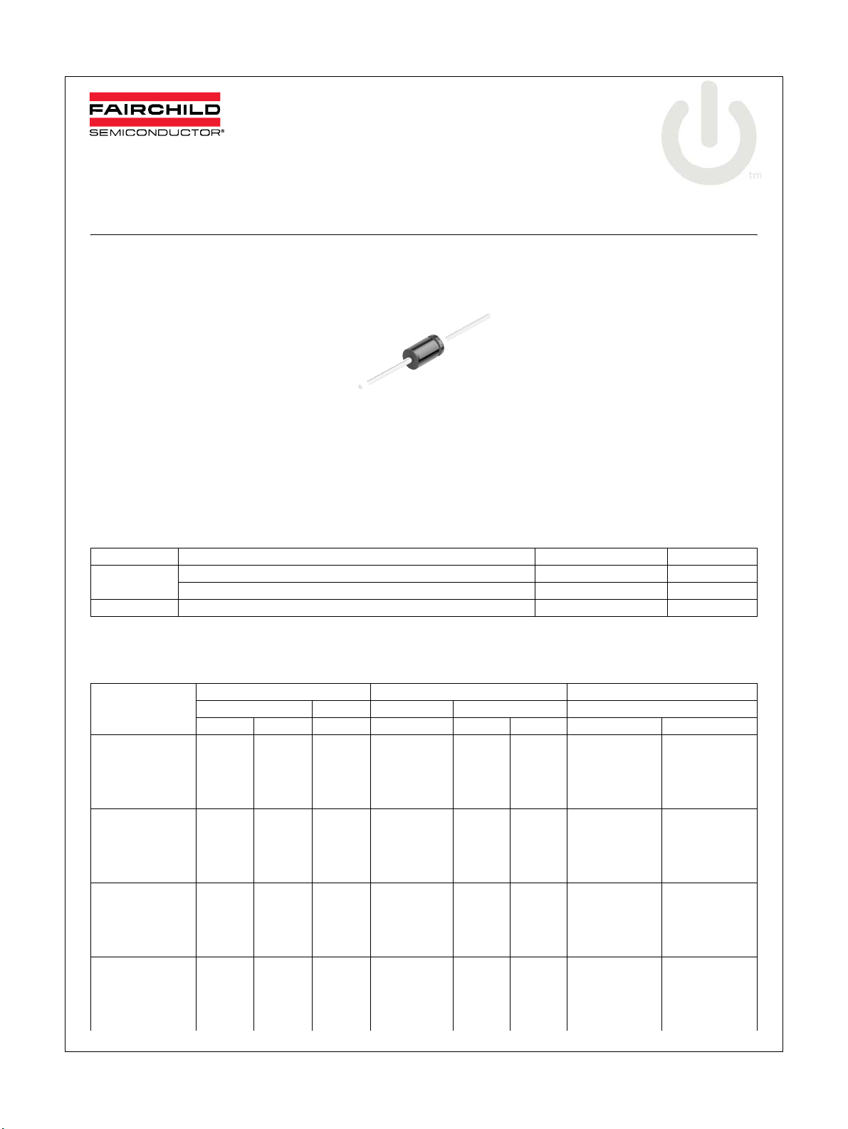
COLOR BAND DENOTES CATHODE
Tolerance = 5%
DO-41 Glass case
BZX85C3V3 - BZX85C56 Zener Diodes
June 2007
Absolute Maximum Ratings * T
Symbol Parameter Value Units
P
D
TJ, T
STG
* These ratings are limiting values above which the serviceability of the diode may be impaired.
Power Dissipation @ TL ≤ 50°C, Lead Length = 3/8” 1.0 W
Derate above 50°C 6.67 mW/°C
Operating and Storage Temperature Range -65 to +200 °C
Electrical Characteristics * T
Zener Voltage (Note 1) Zener Impedance Leakage Current
Device
BZX85C3V3
BZX85C3V6
BZX85C3V9
BZX85C4V3
BZX85C4V7
BZX85C5V1
BZX85C5V6
BZX85C6V2
BZX85C6V8
BZX85C7V5
BZX85C8V2
BZX85C9V1
BZX85C10
BZX85C11
BZX85C12
BZX85C13
BZX85C15
BZX85C16
BZX85C18
BZX85C20
VZ (Volts) I
Min. Max. mA (Ω) (Ω)
3.1
3.4
3.7
4.0
4.4
4.8
5.2
5.8
6.4
7.0
7.7
8.5
9.4
10.4
11.4
12.4
13.8
15.3
16.8
18.8
3.5
3.8
4.1
4.6
5
5.4
6
6.6
7.2
7.9
8.7
9.6
10.6
11.6
12.7
14.1
15.6
17.1
19.1
21.2
= 25°C unless otherwise noted
A
=25°C unless otherwise noted
A
Z
80
60
60
50
45
45
45
35
35
35
25
25
25
20
20
20
15
15
15
10
ZZ @ I
20
15
15
13
13
10
7
4
3.5
3
5
5
7
8
9
10
15
15
20
24
Z
ZZK @ I
400
500
500
500
600
500
400
300
300
200
200
200
200
300
350
400
500
500
500
600
ZK
(mA) μA Max. Volts
1
1
1
1
1
1
1
1
1
0.5
0.5
0.5
0.5
0.5
0.5
0.5
0.5
0.5
0.5
0.5
IR @ V
60
30
5
3
3
1
1
1
1
1
1
1
0.5
0.5
0.5
0.5
0.5
0.5
0.5
0.5
R
1
1
1
1
1.5
2
2
3
4
4.5
5
6.5
7
7.7
8.4
9.1
10.5
11
12.5
14
©2007 Fairchild Semiconductor Corporation 1 www.fairchildsemi.com
BZX85C3V3 - BZX85C56 Rev. F1
Zener Voltage (Note 1) Zener Impedance Leakage Current
Device
BZX85C22
BZX85C24
BZX85C27
BZX85C30
BZX85C33
BZX85C36
BZX85C39
BZX85C43
BZX85C47
BZX85C51
VZ (Volts) I
Z
ZZ @ I
Z
Min. Max. mA (Ω) (Ω)
20.8
22.8
25.1
28
31
34
37
40
44
48
23.3
25.6
28.9
32
35
38
41
46
50
54
10
10
25
25
8
8
8
8
6
6
4
4
30
30
35
40
45
50
90
115
600
600
750
1000
1000
1000
1000
1000
1500
1500
ZZK @ I
ZK
(mA) μA Max. Volts
0.5
0.5
0.25
0.25
0.25
0.25
0.25
0.25
0.25
0.25
0.5
0.5
0.5
0.5
0.5
0.5
0.5
0.5
0.5
0.5
IR @ V
R
BZX85C56 52 60 4 120 2000 0.25 0.5 39
VF Forward Voltage = 1.2V Max @ IF = 200mA
Notes:
1.Zener Voltage (VZ)
The zener voltage is measured with the device junction in the thermal equilibrium at the lead temperature (TL) at 30°C ± 1°C and 3/8” lead length.
Top Mark Information
Device Line 1 Line 2 Line 3 Line 4 Line 5
BZX85C3V3
BZX85C3V6
BZX85C3V9
BZX85C4V3
BZX85C4V7
BZX85C5V1
BZX85C5V6
BZX85C6V2
BZX85C6V8
BZX85C7V5
BZX85C8V2
BZX85C9V1
BZX85C10
BZX85C11
BZX85C12
BZX85C13
BZX85C15
BZX85C16
BZX85C18
BZX85C20
BZX85C22
BZX85C24
BZX85C27
BZX85C30
BZX85C33
BZX85C36
BZX85C39
BZX85C43
BZX85C47
BZX85C51
BZX85C56 LOGO 85C 56 XY
LOGO
LOGO
LOGO
LOGO
LOGO
LOGO
LOGO
LOGO
LOGO
LOGO
LOGO
LOGO
LOGO
LOGO
LOGO
LOGO
LOGO
LOGO
LOGO
LOGO
LOGO
LOGO
LOGO
LOGO
LOGO
LOGO
LOGO
LOGO
LOGO
LOGO
85C
85C
85C
85C
85C
85C
85C
85C
85C
85C
85C
85C
85C
85C
85C
85C
85C
85C
85C
85C
85C
85C
85C
85C
85C
85C
85C
85C
85C
85C
3V3
3V6
3V9
4V3
4V7
5V1
5V6
6V2
6V8
7V5
8V2
9V1
10
11
12
13
15
16
18
20
22
24
27
30
33
36
39
43
47
51
BZX85C3V3 - BZX85C56 Zener Diodes
15.5
17
19
21
23
25
27
30
33
36
XY
XY
XY
XY
XY
XY
XY
XY
XY
XY
XY
XY
XY
XY
XY
XY
XY
XY
XY
XY
XY
XY
XY
XY
XY
XY
XY
XY
XY
XY
BZX85C3V3 - BZX85C56 Rev. F1
2 www.fairchildsemi.com

Top Mark Information (Continued)
BZX85C3V3 - BZX85C56 Zener Diodes
F
47
36
A
XY
F
1st line: F - Fairchild Logo
2nd line: Device Name - 3rd to 4th characters of device name for 1Nxx series
or 4th to 6th characters for BZXyy series
3rd line: Device Name - 5th to 6th characters of device name for 1Nxx se ries
or Voltage rating for BZXyy series
4th line: Device Name - 7th to 8th characters of device name for 1Nxx series
or Large Die identification only for BZ X yy ser i es
5th line: Date Code - Two Digit - Six Weeks Date Code
General Requirements:
1.0 Cathode Band
2.0 First Line: F - Fairchild Logo
3.0 Second Line: Device name - For 1Nxx series: 3rd to 4th characters of the device name.
4.0 Third Line: Device name - For 1Nxx series: 5th to 6th characters of the device name.
5.0 Third Line: Device name - For 1Nxx series: 7th to 8th characters of the device name.
6.0 Fourth Line: Date Code - Two Digit - Six Weeks Date Code
7.0 Devices shall be marked as required in the device specification (PID or FSC Test Spec).
8.0 Maximum no. of marking lines: 5
9.0 Maximum no. of digits per line: 3
10.0 FSC logo must be 20 % taller than the alphanumeric marking and should occupy the 2 characters of the specified line.
11.0 Marking Font: Arial (Except FSC Logo)
12.0 First character of each marking line must be aligned vertically
13.0 All device markings must be based on Fairchild device specification.
For BZxx series: 4th to 6th characters of the device name.
For BZXyy series: Voltage rating
(the 8th character is the large die identification)
For BZXyy series: Large Die Identification character
Where: X represents the last digit of the calendar year
Y represents the Six weeks numeric code
BZX85C3V3 - BZX85C56 Rev. F1
3 www.fairchildsemi.com

TRADEMARKS
The following are registered and unregistered trademarks Fairchild Semiconductor owns or is authorized to use and is not intended to
be an exhaustive list of all such trademarks.
ACEx™
Across the board. Around the world.™
ActiveArray™
Bottomless™
Build it Now™
CoolFET™
CROSSVOLT™
CTL™
Current Transfer Logic™
DOME™
2
E
CMOS™
EcoSPARK
®
EnSigna™
FACT Quiet Series™
®
FACT
®
FAST
FASTr™
FPS™
FRFET™
GlobalOptoisolator™
GTO™
HiSeC™
i-Lo™
ImpliedDisconnect™
IntelliMAX™
ISOPLANAR™
MICROCOUPLER™
MicroPak™
MICROWIRE™
MSX™
MSXPro™
OCX™
OCXPro™
OPTOLOGIC
OPTOPLANAR™
®
®
PACMAN™
POP™
Power220
Power247
®
®
PowerEdge™
PowerSaver™
PowerTrench
Programmable Active Droop™
QFET
®
®
QS™
QT Optoelectronics™
Quiet Series™
RapidConfigure™
RapidConnect™
ScalarPump™
SMART START™
SPM™
SuperFET™
SuperSOT™-3
SuperSOT™-6
SuperSOT™-8
TCM™
The Power Franchise
®
TinyBoost™
TinyBuck™
TinyLogic
®
TINYOPTO™
TinyPower™
TinyWire™
TruTranslation™
μSerDes™
®
UHC
UniFET™
VCX™
Wire™
BZX85C3V3 - BZX85C56 Zener Diodes
BZX85C3V3 - BZX85C56 Zener Diodes
DISCLAIMER
FAIRCHILD SEMICONDUCTOR RESERVES THE RIGHT TO MAKE CHANGES WITHOUT FURTHER NOTICE TO ANY PRODUCTS HEREIN TO
IMPROVE RELIABILITY, FUNCTION OR DESIGN. FAIRCHILD DOES NOT ASSUME ANY LIABILITY ARISING OUT OF THE APPLICATION OR USE
OF ANY PRODUCT OR CIRCUIT DESCRIBED HEREIN;NEITHER DOES IT CONVEY ANY LICENSE UNDER ITS PATENT RIGHTS, NOR THE
RIGHTS OF OTHERS. THESE SPECIFICATIONS DO NOT EXPAND THE TERMS OF FAIRCHILD’S WORLDWIDE TERMS AND CONDITIONS, SPECIFICALLY THE WARRANTY THEREIN, WHICH COVERS THESE PRODUCTS.
LIFE SUPPORT POLICY
FAIRCHILD’S PRODUCTS ARE NOT AUTHORIZED FOR USE AS CRITICAL COMPONENTS IN LIFE SUPPORT DEVICES OR SYSTEMS WITHOUT
THE EXPRESS WRITTEN APPROVAL OF FAIRCHILD SEMICONDUCTOR CORPORATION.
As used herein:
1. Life support devices or systems are devices or systems which, (a) are
intended for surgical implant into the body, or (b) support or sustain life, or
(c) whose failure to perform when properly used in accordance with
instructions for use provided in the labeling, can be reasonably expected
to result in significant injury to the user.
2. A critical component is any component of a life supp ort device or system
whose failure to perform can be reasonably expected to cause the failure
of the life support device or system, or to affect its safet y or effectiven ess.
PRODUCT STATUS DEFINITIONS
Definition of Terms
Datasheet Identification Product Status Definition
Advance Information Formative or In Design This datasheet contains the design specifications for product develop-
Preliminary First Production This datasheet contains preliminary data, and supplement ary data will
No Identification Needed Full Production This datasheet contains final specifications. Fairchild Semiconductor
Obsolete Not In Production This datasheet contains specificat ions on a product that has been dis-
ment. Specifications may change in any manner without notice.
be published at a later date.Fairchild Semiconductor reserves the right
to make changes at any time without notice in order to improve design.
reserves the right to make changes at any time without notice in order
to improve design.
continued by Fairchild semiconductor.The datasheet is printed for reference information only.
BZX85C3V3 - BZX85C56 Rev. F1
Rev. I23
4 www.fairchildsemi.com
 Loading...