

Page 1
www.fairchildsemi.com
AN-8036
FAN5353 / FAN5354 Evaluation Board User Guide
Summary
The FAN5353/54 evaluation board is a compact circuit
including Fairchild’s FAN5353/54 adjustable output (V
by default set to 1.2V), step-down switching voltage
regulator in a 12-Lead MLP 3x3.5 Package.
One 10µF input capacitor, 2 x 10µF output capacitors, and
one 0.47µH inductor are installed on the board to ensure
tight regulation, low ripple, and excellent transient response.
The FAN5353/54 evaluation board provides probe access
points to all key circuit nodes so that electrical
characteristics can be measured.
OUT
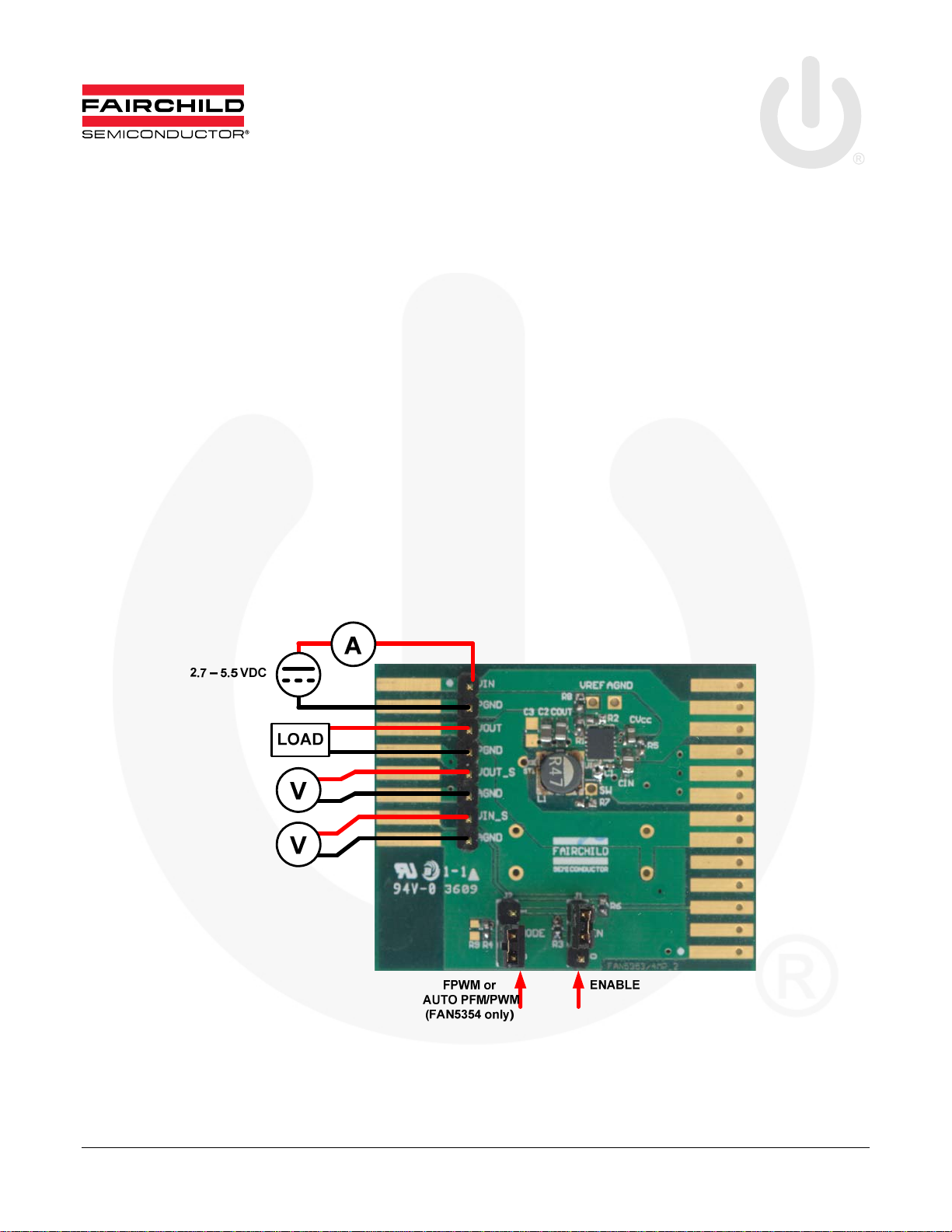
Quick Start Connection Guide
1. Connect VIN input power supply as shown in Figure 1.
2. ENABLE Jumper (J1) factory installed.
3. Connect the external load between VOUT and PGND.
4. Kelvin connected input and output voltage sense points
(VIN_S, VOUT_S) are provided.
5. For FAN5354 only: the jumper “MODE” (J2) in
position 1 selects forced PWM, while in position 0
(factory installed) selects PFM
Figure 1. Evaluation Board Connection Diagram
© 2010 Fairchild Semiconductor Corporation www.fairchildsemi.com
Rev. 1.0.0 • 3/31/10
Page 2
AN-8036 APPLICATION NOTE
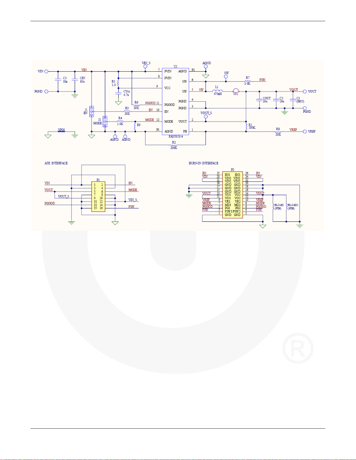
Schematic
Figure 2. Schematic Diagram
© 2010 Fairchild Semiconductor Corporation www.fairchildsemi.com
Rev. 1.0.0 • 3/31/10 2
Page 3
AN-8036 APPLICATION NOTE
FAN5353 Bill of Materials
Reference Quantity Description Manufacturer / Number
U1 1 IC, FAN5353 (MLP 3x3.5mm,14 pin) Fairchild / FAN5353MPX
Vishay / IHLP1616ABERR47M01
L1 1 0.47µH, 4A, 20mΩ 4.9x5.5mm
C1 1 10nf, 25V, 10%, X7R, 0402 DigiKey / PCC1725
CIN, C
, C2 3 10µf, 10V, 10%, X7R, 0805
OUT
CVCC 1 4.7µf, 6.3V, 20%, X5R, 0603
R3, R6, R8 3 20K, 5%, 0603 DigiKey / P20K G
R5 1 1Ω, 5%, 0603 DigiKey / P1.0 G
R9 1 0Ω, 5%, 0603 DigiKey / P0.0 G
R7 1 1.0K, 5%, 0603 DigiKey / P1.0K G
R1 1 100K, 1%, 0603 DigiKey / P100K H
R2 1 200K, 1%, 0603 DigiKey / P200K H
SW, VIN, V
, V
OUT
OUT_S
IN_S
, V
REF
11 1x1 Header Strip, 125C DigiKey / SAM1098-01 V
PGND (2), AGND (3)
J1 1 3x1 Header Strip, 125C DigiKey / SAM1098-03
EN (1) 1 Shunt, Header DigiKey / WM23943
1 PCB, FAN5353/4 MP_2
C3 1 Optional 0805
R
R
LOAD
LOAD
, R
, R
4 No Load Straight Interconnects, SIP DigiKey / ED7150
LOAD1
2 No Load 2.2Ω, 5%, Through Hole DigiKey / PPC2.2W-2CT
LOAD1
Total 37
MURATA / LQH55PNR47NT0
TDK / VLC5020TDC-R47N
Murata / GRM21BR71A106KE51L
DigiKey / 490-3905-1
Murata / GRM188R60J475M
Digikey / 490-3297-1
© 2010 Fairchild Semiconductor Corporation www.fairchildsemi.com
Rev. 1.0.0 • 3/31/10 3
Page 4

AN-8036 APPLICATION NOTE
FAN5354 Bill of Materials
Reference Quantity Description Manufacturer / Number
U1 1 IC, FAN5354 (MLP 3x3.5mm,12 pin) Fairchild / FAN5354MPX
Vishay / IHLP1616ABER47M01
L1 1 0.47µH, 4A, 20mΩ 4.9x5.5mm
MURATA / LQH55PNR47NT0
TDK / VLC5020T-R47N
C1 1 10nF, 25V, 10%, X7R, 0402 DigiKey / PCC1725
Murata / GRM21BR71A106KE51L
CIN, C
, C2 3 10µF, 10V, 10%, X7R, 0805
OUT
DigiKey / 490-3905-1
Murata / GRM188R60J475M
CVCC 1 4.7µF, 6.3V, 20%, X5R, 0603
Digikey / 490-3297-1
R3, R6, R8 3 20K, 5%, 0603 DigiKey / P20K G
R5 1 1Ω, 5%, 0603 DigiKey / P1.0 G
R4, R7 2 1.0K, 5%, 0603 DigiKey / P1.0K G
R1 1 100K, 1%, 0603 DigiKey / P100K H
1
200K, 1%, 0603 DigiKey / P200K H
11 1x1 Header Strip, 125C DigiKey / SAM1098-01
SW, VIN, V
V
, V
OUT
R2
OUT_S
IN_S
, V
REF
PGND (2), AGND (3)
J1, J2
EN (1), MODE (0)
2
3x1 Header Strip, 125C DigiKey / SAM1098-03
2
Shunt, Header DigiKey / WM23943
1 PCB, FAN5353/4 MP_2
R9 1 Optional 0603
C3 1 Optional 0805
R
R
LOAD
LOAD
, R
, R
LOAD1
2 Optional 2.2Ω, 5%, Through Hole
LOAD1
4
Optional Straight Interconnects, SIP DigiKey / ED7150
DigiKey / PPC2.2W-2CT
TOTAL 39
© 2010 Fairchild Semiconductor Corporation www.fairchildsemi.com
Rev. 1.0.0 • 3/31/10 4
Page 5

AN-8036 APPLICATION NOTE
Figure 3. FAN5354 PCB (Top Layer)
© 2010 Fairchild Semiconductor Corporation www.fairchildsemi.com
Rev. 1.0.0 • 3/31/10 5
Page 6

AN-8036 APPLICATION NOTE
Evaluation Board Special Features
Output Capacitance
The FAN5353/5354 evaluation board is provided with an
empty location for the addition of another output capacitor.
Enable Jumper (J1)
The ENABLE jumper comes set to the ‘EN’ position by
default. To disable the FAN5353/5354, move the J1 jumper
to the ‘OFF’ position.
Mode Jumper (J2), External Synchronization
The FAN5354 can be set to operate in AUTO PFM-PWM
when this jumper is in “1” position or in FORCED PWM
mode when J2 is in “0” position. If the middle pin of J2 is
toggled (after removing the shunt), the converter
synchronizes its switching frequency to the external
frequency applied.
Power-Good Flag
The PGOOD output (left-side connector pad 2, counting
from the bottom) is an open-drain connected to VIN through
a pull-up resistor, indicating that the IC is in regulation when
its state is HIGH.
Output Voltage Setting
The output voltage is factory preset to 1.2V since
R1=100kΩ and R2=200kΩ.
To set a different V
, R2 should be replaced with another
OUT
resistor, calculated according to:
8.01R
2R
=
•
()
OUT
8.0V
−
(1)
Optional Load Resistors
Two power resistors may be installed on the board in the
dedicated through holes.
On-Board Test Points
Test point pads are available to access the FB voltage (at
V
pad) and the SW node voltage (at SW pad) with
REF
external probes.
ATTENTION: Since the FB node is high impedance, it is
sensitive to external disturbances. Please connect any
measurement devices before the circuit is powered up.
Never touch the FB node with any metal tip; such as a
scope, voltmeter, or handheld probe, when the evaluation
board is powered on. Failure to follow these instructions
may result in permanent damage of the FAN5353/5354.
© 2010 Fairchild Semiconductor Corporation www.fairchildsemi.com
Rev. 1.0.0 • 3/31/10 6
Page 7

AN-8036 APPLICATION NOTE
Related Datasheets
FAN5353 — 3MHz, 3A TinyBuck™ Synchronous Buck Regulator
FAN5354 — 3MHz, 3A TinyBuck™ Synchronous Buck Regulator
DISCLAIMER
FAIRCHILD SEMICONDUCTOR RESERVES THE RIGHT TO MAKE CHANGES WITHOUT FURTHER NOTICE TO ANY PRODUCTS
HEREIN TO IMPROVE RELIABILITY, FUNCTION, OR DESIGN. FAIRCHILD DOES NOT ASSUME ANY LIABILITY ARISING OUT OF THE
APPLICATION OR USE OF ANY PRODUCT OR CIRCUIT DESCRIBED HEREIN; NEITHER DOES IT CONVEY ANY LICENSE UNDER ITS
PATENT RIGHTS, NOR THE RIGHTS OF OTHERS.
LIFE SUPPORT POLICY
FAIRCHILD’S PRODUCTS ARE NOT AUTHORIZED FOR USE AS CRITICAL COMPONENTS IN LIFE SUPPORT DEVICES OR SYSTEMS
WITHOUT THE EXPRESS WRITTEN APPROVAL OF THE PRESIDENT OF FAIRCHILD SEMICONDUCTOR CORPORATION.
As used herein:
1. Life support devices or systems are devices or systems
which, (a) are intended for surgical implant into the body, or
(b) support or sustain life, or (c) whose failure to perform
when properly used in accordance with instructions for use
provided in the labeling, can be reasonably expected to
result in significant injury to the user.
© 2010 Fairchild Semiconductor Corporation www.fairchildsemi.com
Rev. 1.0.0 • 3/31/10 7
2. A critical component is any component of a life support
device or system whose failure to perform can be
reasonably expected to cause the failure of the life support
device or system, or to affect its safety or effectiveness.
 Loading...