

Fairchild 74VHCT14A service manual
=
=
=
=
=
=
=
=
74VHCT14A — Hex Schmitt Inverter
December 2007
74VHCT14A
Hex Schmitt Inverter
Features
■
High speed: t
High noise immunity: V
■
■
Power down protection is provided on all inputs and
outputs
Low noise: V
■
■
Low power dissipation: I
Pin and function compatible with 74HCT14
■
5.0ns (Typ.) at T
PD
IH
1.0V (Max.)
OLP
2.0V, V
2µA (Max.) @ T
CC
A
IL
25°C
0.8V
A
25°C
General Description
The VHCT14A is an advanced high speed CMOS Hex
Schmitt Inverter fabricated with silicon gate CMOS
technology. The VHCT14A contains six independent
inverters which are capable of transforming slowly
changing input signals into sharply defined, jitter-free
output signals.
Protection circuits ensure that 0V to 7V can be applied to
the input pins without regard to the supply voltage and
to the output pins with V
device destruction due to mismatched supply and
input/output voltages. This device can be used to interface 3V to 5V systems and two supply systems such as
battery backup.
0V. These circuits prevent
CC
Ordering Information
Package
Order Number
74VHCT14AM M14A 14-Lead Small Outline Integrated Circuit (SOIC), JEDEC MS-012,
74VHCT14ASJ M14D 14-Lead Small Outline Package (SOP), EIAJ TYPE II, 5.3mm Wide
74VHCT14AMTC MTC14 14-Lead Thin Shrink Small Outline Package (TSSOP), JEDEC
Device also available in Tape and Reel. Specify by appending suffix letter “X” to the ordering number.
Number Package Description
0.150" Narrow
MO-153, 4.4mm Wide
All packages are lead free per JEDEC: J-STD-020B standard.
©1998 Fairchild Semiconductor Corporation www.fairchildsemi.com
74VHCT14A Rev. 1.5.0
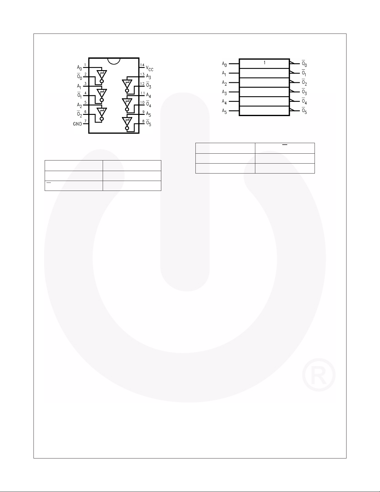
74VHCT14A — Hex Schmitt Inverter
Connection Diagram
Pin Description
Pin Names Description
A
n
O
n
Inputs
Outputs
Logic Symbol
Truth Table
AO
LH
HL
©1998 Fairchild Semiconductor Corporation www.fairchildsemi.com
74VHCT14A Rev. 1.5.0 2
=
<
>
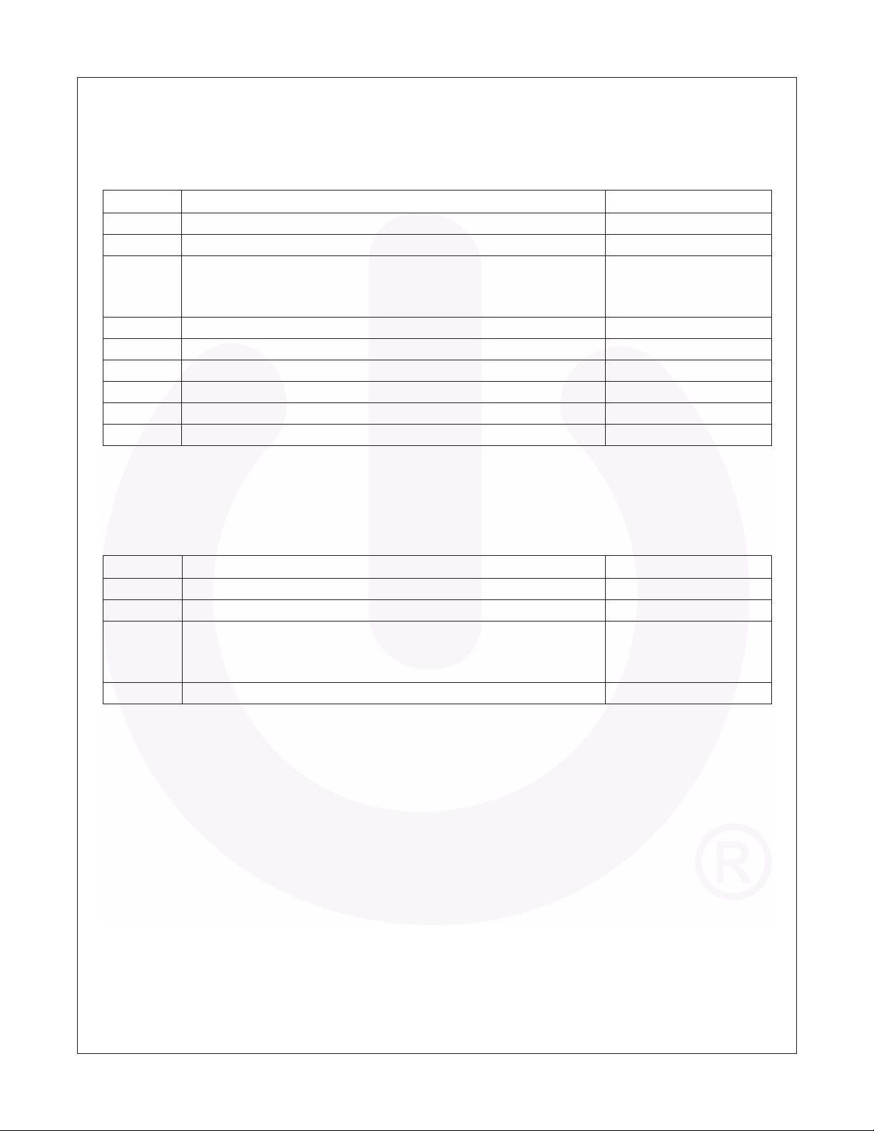
Absolute Maximum Ratings
Stresses exceeding the absolute maximum ratings may damage the device. The device may not function or be
operable above the recommended operating conditions and stressing the parts to these levels is not recommended.
In addition, extended exposure to stresses above the recommended operating conditions may affect device reliability.
The absolute maximum ratings are stress ratings only.
Symbol Parameter Rating
V
I
T
V
V
OUT
I
I
OK
OUT
I
CC
STG
T
CC
IN
IK
Supply Voltage –0.5V to +7.0V
DC Input Voltage –0.5V to +7.0V
DC Output Voltage
Note 1
–0.5V to V
Note 2
Input Diode Current –20mA
Output Diode Current
(3)
DC Output Current ±25mA
DC V
/ GND Current ±50mA
CC
Storage Temperature –65°C to +150°C
Lead Temperature (Soldering, 10 seconds) 260°C
L
+ 0.5V
CC
–0.5V to 7.0V
±20mA
74VHCT14A — Hex Schmitt Inverter
Recommended Operating Conditions
(4)
The Recommended Operating Conditions table defines the conditions for actual device operation. Recommended
operating conditions are specified to ensure optimal performance to the datasheet specifications. Fairchild does not
recommend exceeding them or designing to absolute maximum ratings.
Symbol Parameter Rating
V
CC
V
IN
V
OUT
T
OPR
Notes:
1. HIGH or LOW state. I
2. V
CC
3. V
OUT
4. Unused inputs must be held HIGH or LOW. They may not float.
Supply Voltage 4.5V to +5.5V
Input Voltage 0V to +5.5V
Output Voltage
Note 1
Note 2
Operating Temperature –40°C to +85°C
absolute maximum rating must be observed.
OUT
0V.
GND, V
OUT
V
(Outputs Active).
CC
0V to V
0V to +5.5V
CC
©1998 Fairchild Semiconductor Corporation www.fairchildsemi.com
74VHCT14A Rev. 1.5.0 3
 Loading...