

Fairchild 74VHCT00A service manual
查询74VHCT00A供应商
74VHCT00A
Quad 2-Input NAND Gate
74VHCT00A Quad 2-Input NAND Gate
July 1997
Revised March 1999
General Description
The VHCT00A is an advanced hi gh-speed CMO S 2-Input
NAND Gate fabricated with silicon gate CMOS technology.
It achieves the high-speed operation similar to equi valent
Bipolar Schottky TTL while maintaining the CMOS low
power dissipation. The internal circuit is composed of 3
stages, including bu ffer output, which provide high noise
immunity and stable output.
Protection circuits ensu re that 0V to 7 V can be applied to
the input pins without reg ard to the supply voltage an d to
the output pins with V
device destruction due to mismatched supply and input/
output voltages. This dev ice can be use d to inte rfa ce 3V to
= 0V. These circuits prevent
CC
5V systems and two supply systems such as battery
backup.
Features
■ Hi gh spee d: tPD = 5.0 ns (typ) at TA = 25°C
■ High noise immunity: V
■ Power down protection is provided on all inputs and
outputs
■ Low noise: V
■ Low power dissipation:
I
CC
■ Pin and function compatible with 74HCT00
OLP
= 2 µA (max) at TA = 25°C
= 2.0V, VIL = 0.8V
IH
= 0.8V (max)
Ordering Code:
Order Number Package Number Package Description
74VHCT00AM M14A 14-Lead Small Outline Integrated Circuit (SOIC), JEDEC MS-120, 0.150 Narrow
74VHCT00ASJ M14D 14-Lead Small Outline Package (SOP), EIAJ TYPE II, 5.3mm Wide
74VHCT00AMTC MTC14 14-Lead Thin Shrink Small Outline Package (TSSOP), JEDEC MO-153, 4.4mm Wide
74VHCT00AN N14A 14-Lead Plastic Dual-In-Line Package (PDIP), JEDEC MS-001, 0.300 Wide
Surface mount pack ages are also available on Tape and Reel. Specify by appendi ng the suffix letter “X” to the ordering code.
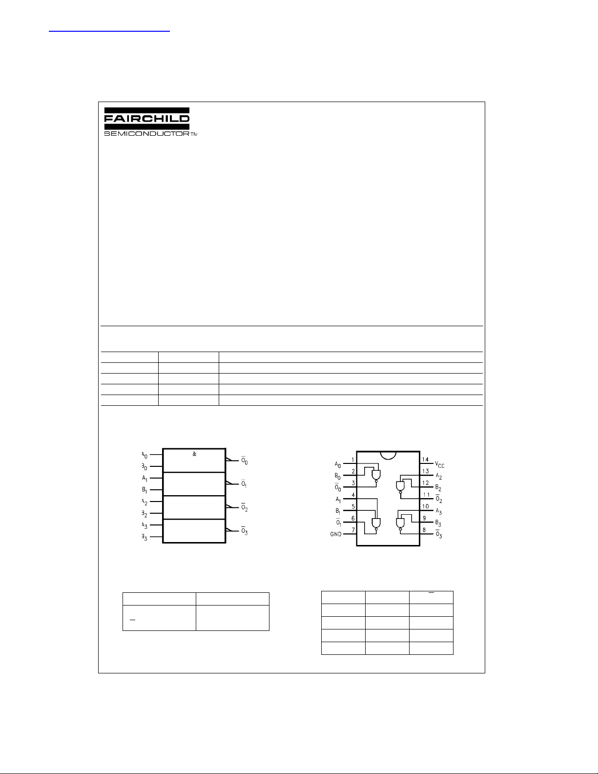
Logic Symbol
Connection Diagram
Pin Descriptions
Pin Names Description
, B
A
n
n
O
n
© 1999 Fairchild Semiconductor Corporation DS500023.prf www.fairchildsemi.com
Inputs
Outputs
Truth T able
ABO
LLH
LHH
HLH
HHL
Absolute Maximum Ratings(Note 1) Recommended Operating
Supply Voltage (VCC) −0.5V to +7.0V
DC Input Voltage (V
DC Output Voltage (V
74VHCT00A
(Note 2) −0.5V to V
) −0.5V to +7.0V
IN
)
OUT
(Note 3) −0.5V to 7.0V
Input Diode Current (I
Output Diode Current (I
) −20 mA
IK
)
OK
(Note 4) ±20 mA
DC Output Current (I
/GND Current (ICC) ±50 mA
DC V
CC
Storage Temperature (T
Lead Temperature (T
) ±25 mA
OUT
) −65°C to +150°C
STG
)
L
(Soldering, 10 seconds) 260°C
CC
+ 0.5V
Conditions
Supply Voltage (V
Input Voltage (V
Output Voltage (V
(Note 2) 0V to V
(Note 3) 0V to 5.5V
Operating Temperature (T
Input Rise and Fall Time (t
= 5.0V ± 0.5V 0 ns/V ∼ 20 ns/V
V
CC
Note 1: Absolute Maximum Ratings are values beyond which the device
may be damaged or ha ve its useful li fe impaire d. The datab ook specific ations should be met, without exception, to ensure that the system design is
reliable over its p ower supp ly, temperature, and ou tput/input loading variables. Fairchild does not recom mend operation outs ide databook specifications.
Note 2: HIGH or LOW state. I
observed.
Note 3: V
Note 4: V
Note 5: Unused inputs must be held HIGH or LOW. They may not float.
CC
OUT
= 0V.
(Note 5)
) 4.5V to 5.5V
CC
)0V to +5.5V
IN
)
OUT
) −40°C to +85°C
OPR
, tf)
r
absolute maximum rating must be
OUT
< GND, V
> VCC (Outputs Active)
OUT
DC Electrical Characteristics
Symbol Parameter
V
V
V
V
I
I
I
I
IH
IL
OH
OL
IN
CC
CCT
OFF
HIGH Level Input Voltage 4.5 2.0 2.0
LOW Level Input Voltage 4.5 0.8 0.8
HIGH Level Output Voltage 4.5 4.40 4.50 4.40 V VIN = VIHIOH = −50 µA
LOW Level Output Voltage 4.5 0.0 0.1 0.1 V VIN = VIHIOL = 50 µA
Input Leakage Current 0 − 5.5 ±0.1 ±1.0 µAVIN = 5.5V or GND
Quiescent Supply Current 5.5 2.0 20.0 µAVIN = VCC or GND
Maximum ICC/ Input
Output Leakage Current 0.0 0.5 5.0 µAV
(Power Down State)
V
CC
(V)
5.5 2.0 2.0
5.5 0.8 0.8
4.5 3.94 3.80 V or VILIOH = −8 mA
4.5 0.36 0.44 V or VILIOL = 8 mA
5.5 1.35 1.50 mA
TA = 25°CT
Min Typ Max Min Max
= −40°C to +85°C
A
Units Conditions
V
V
VIN = 3.4V
Other Inputs = VCC or GND
= 5.5V
OUT
CC
Noise Characteristics
V
Symbol Parameter
V
OLP
(Note 6)
V
OLV
(Note 6)
V
IHD
(Note 6)
V
ILD
(Note 6)
Note 6: Paramete r guaranteed by design.
Quiet Output Maximum Dynamic V
Quiet Output Minimum Dynamic V
Minimum HIGH Level Dynamic Input Voltage
Maximum LOW Level Dynamic Input Voltage
OL
OL
www.fairchildsemi.com 2
CC
(V)
5.0 0.4 0.8 V CL = 50 pF
5.0 −0.4 −0.8 V CL = 50 pF
5.0 2.0 V CL = 50 pF
5.0 0.8 V CL = 50 pF
TA = 25°C
Typ Limit
Units Conditions
 Loading...