Fairchild 74VHC4051 service manual

April 1994
Revised April 1999
74VHC4051 • 74VHC4052 • 74VHC4053
8-Channel Analog Multiplexer • Dual 4-Channel Analog
Multiplexer • Triple 2-Channel Analog Multiplexer
74VHC4051 • 74VHC4052 • 74VHC4053 8-Channel Analog Multiplexer • Dual 4-Channel Analog Multip lexer • T ripl e
2-Channel Analog Multiplexer
General Description
These multiplexers are digitall y controlled analog sw itches
implemented in adva nced silicon-gate CMOS technology.
These switches have low “on” resistance and low “off” leakages. They are bidirectional switches, thus any analog
input may be used as an output an d vice- ver sa. A lso the se
switches contain linearization circuitry which lowers the
“on” resistance and increases switch linearity. These
devices allow control of up to ±6V (peak) analo g signals
with digital control signals of 0 to 6V. Three supply pins are
provided for V
nection of 0–5V logic signals when V
input range of ±5V when V
have an inhibit control which when high will disable all
switches to their off state. All a nalog inputs and outputs
and digital inputs are protected from e lectrostatic damage
by diodes to V
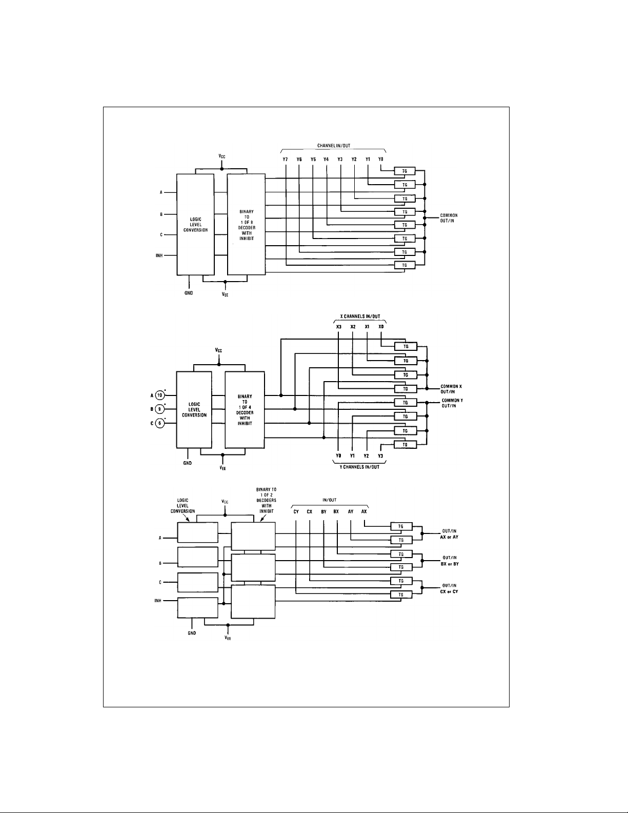
VHC4051: This devi ce connects together the outputs of 8
switches, thus achieving an 8 channel Multiplexer. The
binary code placed on the A , B, and C select lines dete rmines which one o f the eight switches is “on”, and connects one of the eight inputs to the common output.
VHC4052: This devi ce connects together the outputs of 4
switches in two sets, thu s achieving a pair of 4-channel
, ground, and VEE. This enables the con-
CC
and ground.
CC
EE
= 5V and an analog
CC
= 5V. All three devices also
multiplexers. The binary code placed on the A, and B
select lines determine which switch in each 4 channel section is “on”, connecting one of the four inputs in each section to its common output. This enables the implementation
of a 4-channel differential multiplexer.
VHC4053: This device conta ins 6 switches who se outputs
are connected together in pai rs, thus impl ementing a tri ple
2 channel multiplexer, or the equivalent of 3 single-poledouble throw confi gurations. Each of the A, B, o r C select
lines independently co ntr ols on e pa ir of swi tche s, selecting
one of the two switches to be “on”.
Features
■ Wide analog input voltage range: ±6V
■ Low “on” resistance: 50 typ. (V
CC–VEE
= 9V)
30 typ. (V
■ Logic level translat ion to enabl e 5V logi c with ±5V ana-
log signals
■ Low quiescent current: 80 µA maximum
■ Matched switch characteristic
■ Pin and function compatible with the 74HC4051/ 4052/
4053
CC–VEE
= 4.5V)
Ordering Code:
Order Number Package Number Package Description
74VHC4051M M16A 16-Lead Small Outline Integrated Circuit (SOIC), JEDEC MS-012, 0.150” Narrow
74VHC4051WM M16B 16-Lead Small Outline Integrated Circuit (SOIC), JEDEC MS-013, 0.300” Wide
74VHC4051MTC MTC16 16-Lead Thin Shrink Small Outline Package (TSSOP), JEDEC MO-153, 4.4mm Wide
74VHC4051N N16E 16-Lead Plastic Dual-In-Line Package (PDIP), JEDEC MS-001, 0.300” Wide
74VHC4052M M16A 16-Lead Small Outline Integrated Circuit (SOIC), JEDEC MS-012, 0.150” Narrow
74VHC4052WM M16B 16-Lead Small Outline Integrated Circuit (SOIC), JEDEC MS-013, 0.300” Wide
74VHC4052MTC MTC16 16-Lead Thin Shrink Small Outline Package (TSSOP), JEDEC MO-153, 4.4mm Wide
74VHC4052N N16E 16-Lead Plastic Dual-In-Line Package (PDIP), JEDEC MS-001, 0.300” Wide
74VHC4053M M16A 16-Lead Small Outline Integrated Circuit (SOIC), JEDEC MS-012, 0.150” Narrow
74VHC4053WM M16B 16-Lead Small Outline Integrated Circuit (SOIC), JEDEC MS-013, 0.300” Wide
74VHC4053MTC MTC16 16-Lead Thin Shrink Small Outline Package (TSSOP), JEDEC MO-153, 4.4mm Wide
74VHC4053N N16E 16-Lead Plastic Dual-In-Line Package (PDIP), JEDEC MS-001, 0.300” Wide
Surface mount pack ages are also available on Tape and Reel. Sp ec if y by appending the suffix letter “X” to the ordering code.
© 1999 Fairchild Semiconductor Corporation DS011674.prf www.fairchildsemi.com

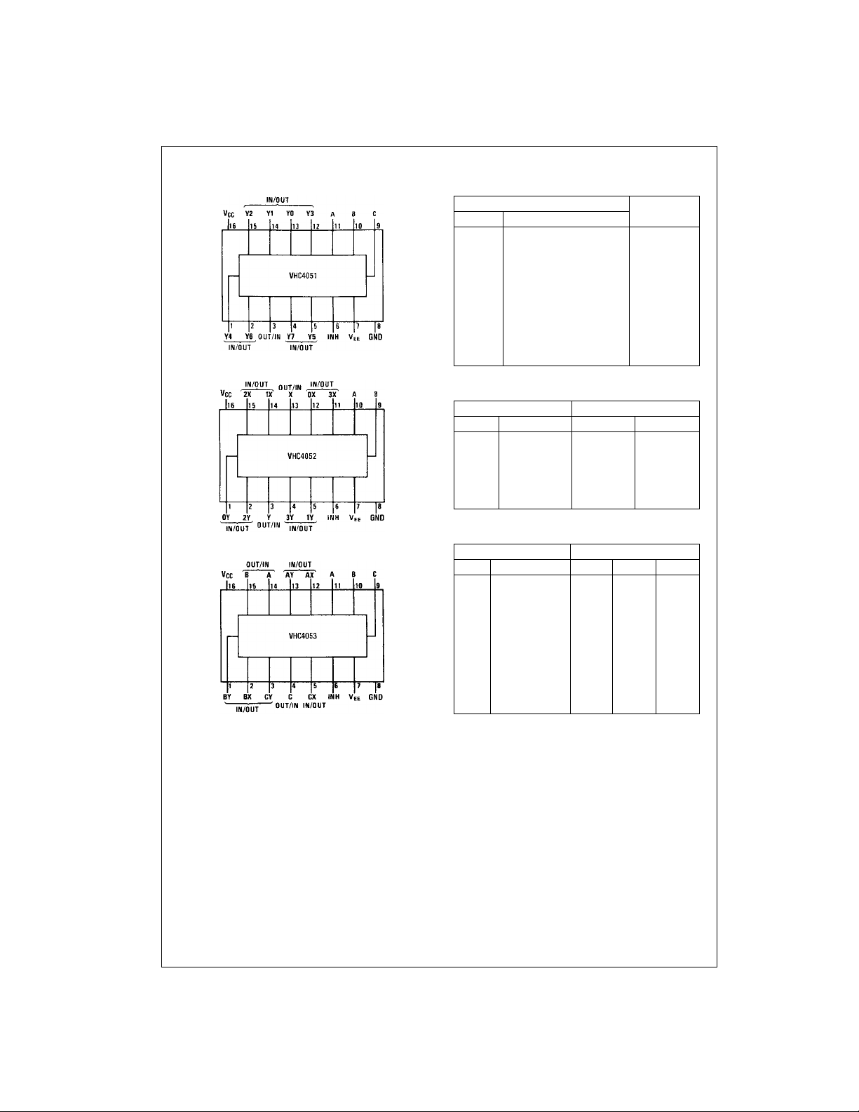
Connection Diagrams
Top View
74VHC4051 • 74VHC4052 • 74VHC4053
Truth Tables
4051
Input “ON”
INHCBAChannel
H XXX None
L LLL Y0
LLLH Y1
LLHL Y2
LLHH Y3
LHLL Y4
LHLH Y5
LHHL Y6
L HHH Y7
4052
Inputs “ON” Channels
INH B A X Y
HXXNone None
LLL 0X 0Y
LLH 1X 1Y
LHL 2X 2Y
LHH 3X 3Y
Top View
Top View
4053
Input “ON” Channels
INHCBA C B A
H X X X None None None
L L L L CX BX AX
LLLHCX BX AY
L L H L CX BY AX
LLHHCX BY AY
L H L L CY BX AX
LHLHCY BX AY
L H H L CY BY AX
L HHH CY BY AY
www.fairchildsemi.com 2

Logic Diagrams
74VHC4051 • 74VHC4052 • 74VHC4053
74VHC4051
74VHC4052
74VHC4053
3 www.fairchildsemi.com

Absolute Maximum Ratings(Note 1)
(Note 2)
Supply Voltage (VCC) −0.5 to +7.5V
Supply Voltage (V
Control Input Voltage (V
Switch I/O Voltage (V
Clamp Diode Current (I
Output Current, per pin (I
or GND Current, per pin (ICC) ±50 mA
V
CC
) +0.5 to −7.5V
EE
) −1.5 to VCC+1.5V
IN
)V
IO
, IOK) ±20 mA
IK
) ±25 mA
OUT
−0.5 to VCC+0.5V
EE
Storage Temperature Range
) −65°C to +150°C
(T
STG
Power Dissipation (P
)
D
(Note 3) 600 mW
S.O. Package only 500 mW
Lead Temperature (T
)
L
(Soldering 10 second s) 260°C
74VHC4051 • 74VHC4052 • 74VHC4053
Recommended Operating
Conditions
Min Max Units
Supply Voltage (V
Supply Voltage (V
DC Input or Output Voltage 0 V
, V
(V
IN
OUT
Operating Temperature Range
) −40 +85 °C
(T
A
Input Rise or Fall Times
, tf)
(t
r
= 2.0V 1000 ns
V
CC
= 4.5V 500 ns
V
CC
= 6.0V 400 ns
V
CC
Note 1: Absolute Maximum Ratings are those values beyond which damage to the device may occur.
Note 2: Unless otherwise specified all voltages are referenced to ground.
Note 3: Power Dissipation tem perature de rating — pla stic “N” pac kage: −
12 mW/°C from 65 °C to 85°C.
)26V
CC
)0−6V
EE
CC
)
V
www.fairchildsemi.com 4
 Loading...