

Fairchild 74VHC373 service manual

tm
=
=
=
=
=
=
=
74VHC373 Octal D-Type Latch with 3-STATE Outputs
April 2007
74VHC373
Octal D-Type Latch with 3-STATE Outputs
Features
■
High Speed: t
High Noise Immunity: V
■
■
Power Down Protection is provided on all inputs
■
Low Noise: V
Low Power Dissipation: I
■
■
Pin and Function Compatible with 74HC373
5.0ns (typ) @ V
PD
0.6V (Typ.)
OLP
V
NIH
NIL
4µA (Max) @ T
CC
CC
28% V
5V
CC
(Min.)
25°C
A
General Description
The VHC373 is an advanced high speed CMOS octal
D-type latch with 3-STATE output fabricated with silicon
gate CMOS technology. It achieves the high speed operation similar to equivalent Bipolar Schottky TTL while
maintaining the CMOS low power dissipation. This 8-bit
D-type latch is controlled by a latch enable input (LE)
and an output enable input (OE
). The latches appear
transparent to data when latch enable (LE) is HIGH.
When LE is LOW, the data that meets the setup time is
LATCHED. When the OE
input is HIGH, the eight
outputs are in a high impedance state.
An input protection circuit ensures that 0V to 7V can be
applied to the input pins without regard to the supply
voltage. This device can be used to interface 5V to 3V
systems and two supply systems such as battery back
up. This circuit prevents device destruction due to mismatched supply and input voltages.
Ordering Information
Package
Order Number
74VHC373M M20B 20-Lead Small Outline Integrated Circuit (SOIC), JEDEC MS-013, 0.300" Wide
74VHC373SJ M20D 20-Lead Small Outline Package (SOP), EIAJ TYPE II, 5.3mm Wide
74VHC373MTC MTC20 20-Lead Thin Shrink Small Outline Package (TSSOP), JEDEC MO-153, 4.4mm
Surface mount packages are also available on Tape and Reel. Specify by appending the suffix letter “X” to the
ordering number. Pb-Free package per JEDEC J-STD-020B.
Number Package Description
Wide
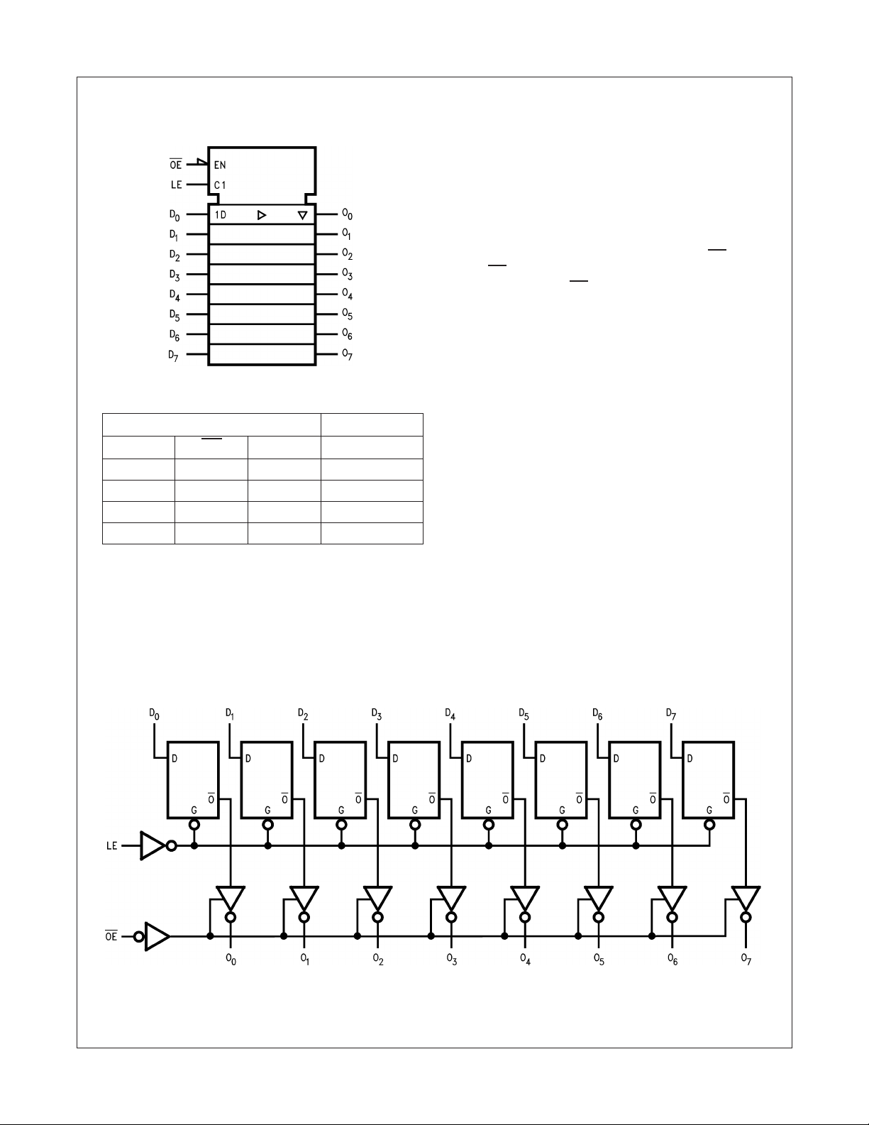
Connection Diagram Pin Descriptions
Pin Names Description
D
–D
0
7
LE Latch Enable Input
OE
–O
O
0
7
©1993 Fairchild Semiconductor Corporation www.fairchildsemi.com
74VHC373 Rev. 1.3
Data Inputs
Output Enable Input
3-STATE Outputs
H =
=
74VHC373 Octal D-Type Latch with 3-STATE Outputs
Logic Symbol
IEEE/IEC
Truth Table
Inputs Outputs
LE OE D
XHX Z
HLL L
HLH H
LLX O
HIGH Voltage Level
L = LOW Voltage Level
Z = High Impedance
X = Immaterial
Previous O
O
0
Latch Enable
before HIGH-to-LOW transition of
0
n
O
Functional Description
The VHC373 contains eight D-type latches with
3-STATE standard outputs. When the Latch Enable (LE)
input is HIGH, data on the D
In this condition the latches are transparent, i.e., a latch
output will change state each time its D input changes.
When LE is LOW, the latches store the information that
was present on the D inputs a setup time preceding the
HIGH-to-LOW transition of LE. The 3-STATE standard
outputs are controlled by the Output Enable (OE
When OE
2-state mode. When OE
are in the high impedance mode but this does not interfere with entering new data into the latches.
n
0
is LOW, the standard outputs are in the
inputs enters the latches.
n
) input.
is HIGH, the standard outputs
Logic Diagram
Please note that this diagram is provided only for the understanding of logic operations and should not be used to
estimate propagation delays.
Figure 1.
©1993 Fairchild Semiconductor Corporation www.fairchildsemi.com
74VHC373 Rev. 1.3 2
=
=
Absolute Maximum Ratings
Stresses exceeding the absolute maximum ratings may damage the device. The device may not function or be
operable above the recommended operating conditions and stressing the parts to these levels is not recommended.
In addition, extended exposure to stresses above the recommended operating conditions may affect device reliability.
The absolute maximum ratings are stress ratings only.
Symbol Parameter Rating
V
V
V
I
I
OUT
I
T
CC
IN
OUT
I
IK
OK
CC
STG
T
Supply Voltage –0.5V to +7.0V
DC Input Voltage –0.5V to +7.0V
DC Output Voltage –0.5V to V
CC
+ 0.5V
Input Diode Current –20mA
Output Diode Current ±20mA
DC Output Current ±25mA
DC V
/GND Current ±75mA
CC
Storage Temperature –65°C to +150°C
Lead Temperature (Soldering, 10 seconds) 260°C
L
74VHC373 Octal D-Type Latch with 3-STATE Outputs
Recommended Operating Conditions
(1)
The Recommended Operating Conditions table defines the conditions for actual device operation. Recommended
operating conditions are specified to ensure optimal performance to the datasheet specifications. Fairchild does not
recommend exceeding them or designing to absolute maximum ratings.
Symbol Parameter Rating
V
CC
V
IN
V
OUT
T
OPR
t
, t
r
Note:
1. Unused inputs must be held HIGH or LOW. They may not float.
Supply Voltage 2.0V to +5.5V
Input Voltage 0V to +5.5V
Output Voltage 0V to V
Operating Temperature –40°C to +85°C
Input Rise and Fall Time,
f
V
CC
V
CC
3.3V ± 0.3V
5.0V ± 0.5V
0ns/V ∼ 100ns/V
0ns/V ∼ 20ns/V
CC
©1993 Fairchild Semiconductor Corporation www.fairchildsemi.com
74VHC373 Rev. 1.3 3
 Loading...