Fairchild 74VCX162240 service manual

查询74VCX162240供应商
74VCX162240
Low Voltage 16-Bit Inverting Buffer/Line Driver with 3.6V
Tolerant Inputs and Outputs and 26 Ω Series Resistors in
Outputs
January 1998
Revised April 1999
74VCX162240 Low Voltage 16-Bit Inverting Buffer/Line Dri ver with 3.6V Tolerant Inputs and Outputs and 26Ω
Series Resistors in Outputs
General Description
The VCX162240 c ontains sixteen in verting buffers with 3STATE outputs to be em ployed as a m emory an d address
driver, clock driver, or bus oriented transmitter/receiver.
The device is nibble (4-bit) controlled. Each nibble has separate 3-STATE control inputs which can be shorted
together for full 16-bit operation.
The 74VCX162240 is designed for low v oltage (1.65V to
3.6V) V
74VCX162240 is also designed with 26Ω series resistors in
the outputs. This design re duces line noise i n applications
such as memory address d rivers, clock drivers, and bus
transceivers/transmitters .
The 74VCX162240 is fab ricated with an advance d CMOS
technology to achieve high speed operation while maintaining low CMOS power dissipation.
applications with I/O capability up to 3.6V. The
CC
Features
■ 1.65V–3.6V VCC supply operation
■ 3.6V tolerant inputs and outputs
■ 26Ω series resistors in outputs
■ t
PD
3.3 ns max for 3.0V to 3.6V V
3.8 ns max for 2.3V to 2.7V VCC
7.6 ns max for 1.65V to 1.95V V
■ Power-off high impedance inputs and outputs
■ Supports live insertion and withdrawal (Note 1)
■ Static Drive (I
±12 mA @ 3.0V V
±8 mA @ 2.3V V
±3 mA @ 1.65V V
■ Uses patented noise/EMI reduction circuitry
■ Latch-up performance exce eds 300 mA
■ ESD performance:
Human body model > 2000V
Machine model > 200V
Note 1: To ensure the high-impedance state d uring power up or power
should be tied to VCC through a pull-up r esistor; the min imum
down, OE
value of the res istor is d eter mine d by the cu rre nt-sou rcin g ca pa bility of t he
driver.
OH/IOL
)
CC
CC
CC
CC
CC
Ordering Code:
Order Number Package Number Package Descriptions
74VCX162240MTD MTD48 48-Lead Thin Shrink Small Outline Package (TSSOP), JECED MO-153, 6.1mm Wide
Devices also availab le in Tape and Reel. Specify by appending th e s uffix let t er “X” to the ordering code.
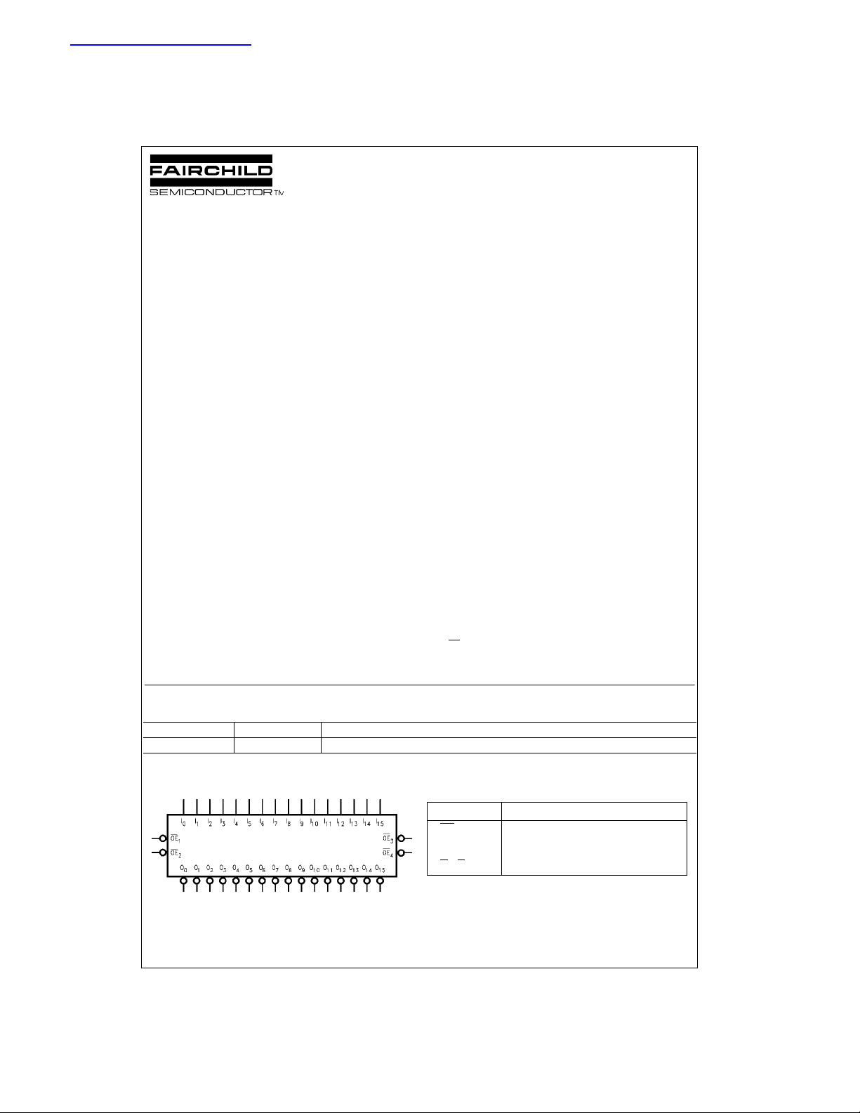
Logic Symbol Pin Descriptions
Pin Names Description
OE
n
I
0–I15
O
0–O15
© 1999 Fairchild Semiconductor Corporation DS500091.prf www.fairchildsemi.com
Output Enable Input (Active LOW)
Inputs
Outputs

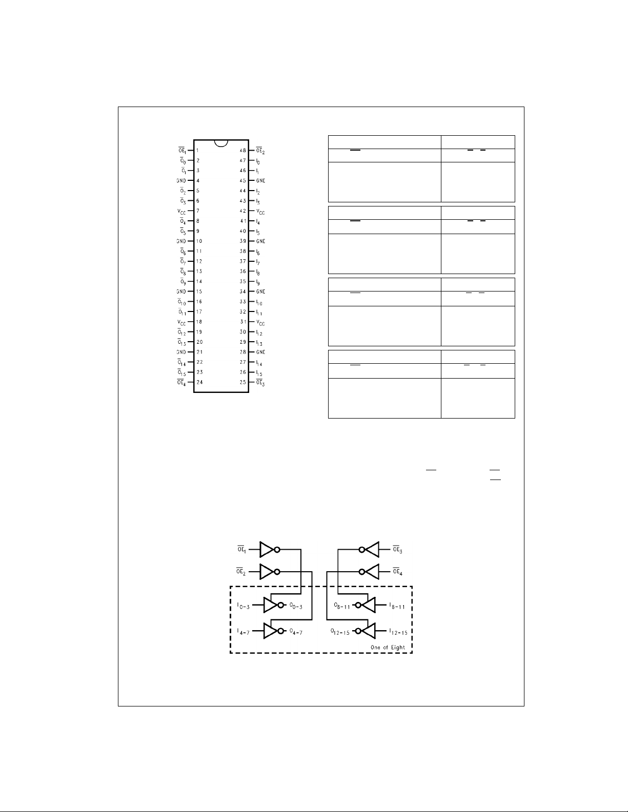
Connection Diagram Truth Tables
OE
74VCX162240
LL H
LH L
HX Z
OE
LL H
LH L
HX Z
OE
LL H
LH L
HX Z
OE
LL H
LH L
HX Z
H = HIGH Voltage Level
L = LOW Voltage Level
X = Immaterial (HIGH or LOW, inputs may not float)
Z = High Impedance
Inputs Outputs
1
I0–I
3
Inputs Outputs
2
I4–I
7
Inputs Outputs
3
I8–I
11
Inputs Outputs
4
I12–I
15
O0–O
O4–O
O8–O
O12–O
3
7
11
15
Functional Description
The 74VCX162240 contains sixteen i nverting buffers with
3-STATE outputs. The device is nibble (4 bits) controlled
with each nibble funct ioning ide ntically, but independent of
each other. The control pins may be shor ted together to
obtain full 16-bit ope ration.The 3-STATE outputs are con -
Logic Diagram
www.fairchildsemi.com 2
trolled by an Output Enable (OE
LOW, the outputs are in the 2-state mode. When OE
) input. When OEn is
n
is
n
HIGH, the standard outputs are in the high impedance
mode but this does not interfere with entering new data into
the inputs.

Absolute Maximum Ratings(Note 2) Recommended Operating
Supply Voltage (VCC) −0.5V to +4.6V
DC Input Voltage (V
Output Voltage (V
) −0.5V to +4.6V
I
)
O
Outputs 3-STATED −0.5V to +4.6V
Outputs Active (Note 3) −0.5V to V
DC Input Diode Current (I
DC Output Diode Current (I
< 0V −50 mA
V
O
> V
V
O
CC
) VI < 0V −50 mA
IK
)
OK
+0.5V
CC
+50 mA
DC Output Source/Sink Current
) ±50 mA
(I
OH/IOL
or GND Current per
DC V
CC
Supply Pin (I
Storage Temperature Range (T
or GND) ±100 mA
CC
) −65°C to +150°C
STG
Conditions
Power Supply
Operating 1.65V to 3.6V
Data Retention Only 1.2V to 3.6V
Input Voltage −0.3V to +3.6V
Output Voltage (V
Output in Active States 0V to V
Output in 3-State 0.0V to 3.6V
Output Current in I
VCC = 3.0V to 3.6V ±12 mA
= 2.3V to 2.7V ±8 mA
V
CC
= 1.65V to 2.3V ±3 mA
V
CC
Free Air Operating Temperature (T
Minimum Input Edge Rate (∆t/∆V)
= 0.8V to 2.0V, VCC = 3.0V 10 ns/V
V
IN
Note 2: The Absolute Maximum Ratings are those values beyond which
the safety of the device cannot be guaranteed. The device should not be
operated at these limits. The parametric values defined in the Electrical
Characteristics tables are not guaranteed at the Absolute Maximum Rat-
ings. The “Recommended Operating Conditions” table will define the conditions for actual device operation.
Absolute Maximum Rating must be observed.
Note 3: I
O
Note 4: Floating or unused inputs m us t be held HIGH or LOW.
(Note 4)
)
O
OH/IOL
) −40°C to +85°C
A
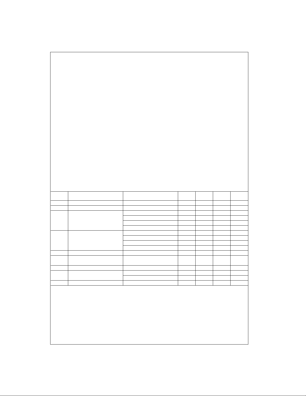
DC Electrical Characteristics (2.7V < VCC ≤ 3.6V)
V
Symbol Parameter Conditions
V
IH
V
IL
V
OH
V
OL
I
I
I
OZ
I
OFF
I
CC
∆I
CC
Note 5: Outputs disab led or 3-STATE only.
HIGH Level Input Voltage 2.7 − 3.6 2.0 V
LOW Level Input Voltage 2.7 − 3.6 0.8 V
HIGH Level Output Voltage IOH = −100 µA2.7 − 3.6 VCC − 0.2 V
LOW Level Output Voltage IOL = 100 µA2.7 − 3.6 0.2 V
Input Leakage Current 0 ≤ VI ≤ 3.6V 2.7 − 3.6 ±5.0 µA
3-STATE Output Leakage 0 ≤ VO ≤ 3.6V
Power-OFF Leakage Current 0 ≤ (VI, VO) ≤ 3.6V 0 10 µA
Quiescent Supply Current VI = VCC or GND 2.7 − 3.6 20 µA
Increase in ICC per Input VIH = VCC −0.6V 2.7 − 3.6 750 µA
IOH = −6 mA 2.7 2.2 V
IOH = −8 mA 3.0 2.4 V
IOH = −12 mA 3.0 2.2 V
IOL = 6 mA 2.7 0.4 V
IOL = 8 mA 3.0 0.55 V
IOL = 12 mA 3.0 0.80 V
VI = VIH or V
VCC ≤ (VI, VO) ≤ 3.6V (Note 5) 2.7 − 3.6 ±20 µA
IL
CC
(V)
2.7 − 3.6 ±10 µA
Min Max Units
74VCX162240
CC
3 www.fairchildsemi.com
 Loading...