Fairchild 74VCX08 service manual

查询74VCX08BQX供应商
74VCX08
Low Voltage Quad 2-Input AND Gate with
3.6V Tolerant Inputs and Outputs
74VCX08 Low Voltage Quad 2-Input AND Gate with 3.6V Tolerant Inputs and Outputs
July 1999
Revised February 2005
General Description
The VCX08 contains four 2-input AN D gates. Thi s product
is designed for low voltage (1.2V to 3. 6V ) V
with I/O compatibility up to 3.6V
The VCX08 is fabricated with an advanced CMOS technol-
ogy to achieve high-sp eed ope ration wh ile m aintainin g low
CMOS power dissipation.
applications
CC
Features
■ 1.2V to 3.6V V
■ 3.6V tolerant inputs and outputs
■ t
PD
2.8 ns max for 3.0V to 3.6V V
■ Power-off high impedance inputs and outputs
■ Static Drive (I
r
24 mA @ 3.0V V
■ Uses patented Quiet Series
circuitry
■ Latchup performance exceeds 300 mA
■ ESD performance:
Human body model ! 2000V
Machine model
■ Leadless Pb-Free DQFN package
supply operation
CC
OH/IOL
Ordering Code:
Order Number
74VCX08M
(Note 1)
74VCX08BQX
(Note 2)
74VCX08MTC
(Note 1)
74VCX08MTCX_NL
(Note 3)
Pb-Free package per JEDEC J-STD-020B.
Note 1: Devices also available in Tape and Reel. Specify by appending the suffix let te r “X” to the ordering code.
Note 2: DQFN package available in Tape and Reel only.
Note 3: “_NL” indicates Pb-Free pac k age (per JEDEC J-S T D -020B). Device available in Tape and Reel only.
Package
Number
M14A 14-Lead Small Outline Integrated Circuit (SOIC), JEDEC MS-012, 0.150" Narrow
MLP014A Pb-Free 14-Terminal Depopulated Quad Very-Thin Flat Pack No Leads (DQFN), JEDEC
MO-241, 2. 5 x 3.0mm
MTC14 14-Lead Thin Shrink Small Outline Package (TSSOP), JEDEC MO-153, 4.4mm Wide
MTC14 Pb-Free 14-Lead Thin Shrink Small Outline Package (TSSOP), JEDEC MO-153, 4.4mm
Wide
Package Descript ion
)
!
250V
CC
¥
noise/EMI reduction
CC
¥
Quiet Series
© 2005 Fairchild Semiconductor Corporation DS500165 www.fairchildsemi.com
is a trademark of Fair child Semiconductor Corporation.

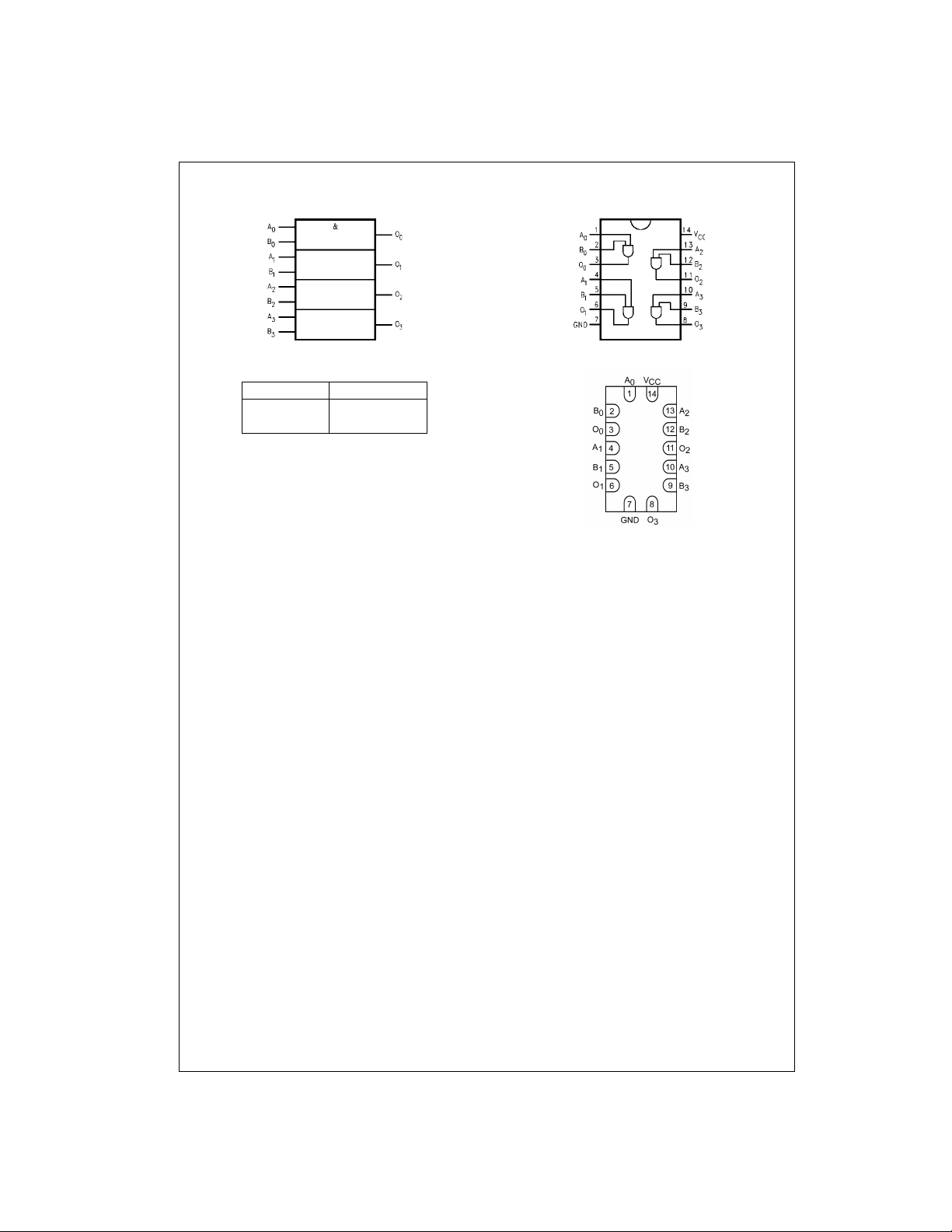
Logic Symbol
Connection Diagrams
74VCX08
Pin Descriptions
Pin Names Description
, B
A
n
n
O
n
IEEE/IEC
Inputs
Outputs
Pin Assignments for SOIC and TSSOP
Pad Assignments for DQFN
(Top View)
www.fairchildsemi.com 2

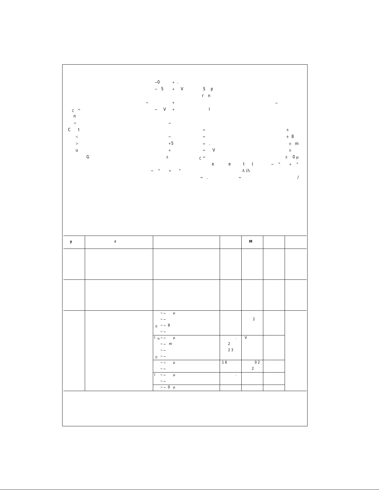
Absolute Maximum Ratings(Note 4) Recommended Operating
Supply Voltage (VCC)
DC Input Voltage (V
Output Voltage (V
)
I
)
O
HIGH or LOW State (Note 5)
0V
V
CC
DC Input Diode Current (I
0V
V
I
DC Output Diode Current (I
V
0V
O
! V
V
O
CC
)
IK
)
OK
DC Output Source/Sink Current (I
DC V
or Ground Current per
CC
Supply Pin (I
or Ground)
CC
Storage Temperature Range (T
stg
OH/IOL
)
0.5V to 4.6V
0.5V to 4.6V
0.5V to VCC 0.5V
0.5V to 4.6V
)
65q
C to 150qC
50 mA
50 mA
50 mA
50 mA
r
100 mA
Conditions
Power Supply
Operating 1.2V to 3.6V
Input Voltage
Output Voltage (V
HIGH or LOW State 0V to V
Output Current in IOH/I
VCC 3.0V to 3.6V
V
2.3V to 2.7V
CC
1.65V to 2.3V
V
CC
1.4V to 1.6V
V
CC
V
1.2V
CC
Free Air Operating Temperature (T
Minimum Input Edge Rate (
V
0.8V to 2.0V, VCC 3.0V 10 ns/V
in
Note 4: The Absolute Maxi mum Ratings are thos e values beyond which
the safety of the d evice cannot b e guaranteed . The device sh ould not be
operated at these lim its. The parametric values defin ed in the Electrical
Characteristics ta bles are not gu aranteed at the Absolute M aximum Rat-
ings. The “Recommended Operating Conditions” table will define the conditions for actual device oper ation.
Absolute Maximum Rating must be observed.
Note 5: I
O
Note 6: Floating or unus ed inputs must be held HI GH or LOW
(Note 6)
)
O
OL
't/'
)
A
V)
DC Electrical Characteristics
V
Symbol Parameter Conditions
V
IH
V
IL
V
OH
HIGH Level Input Voltage 2.7 to 3.6 2.0
LOW Level Input Voltage 2.7 to 3.6 0.8
HIGH Level Output Voltage IOH 100 PA 2.7 to 3.6 VCC - 0.2
IOH 12 mA 2.7 2.2
IOH 18 mA 3.0 2.4
IOH 24 mA 3.0 2.2
IOH 100 PA 2.3 to 2.7 VCC - 0.2
IOH 6 mA 2.3 2.0
IOH 12 mA 2.3 1.8
IOH 18 mA 2.3 1.7
IOH 100 PA 1.65 to 2.3 VCC - 0.2
IOH 6 mA 1.65 1.25
IOH 100 PA 1.4 to 1.6 VCC - 0.2
IOH 2 mA 1.4 1.05
IOH 100 PA1.2V
CC
(V)
2.3 to 2.7 1.6
1.65 to 2.3 0.65 x V
1.4 to 1.6 0.65 x V
1.2 0.65 x V
2.3 to 2.7 0.7
1.65 to 2.3 0.35 x V
1.4 to 1.6 0.35 x V
1.2 0.05 x V
Min Max Units
CC
CC
CC
- 0.2
CC
0.3V to 3.6V
40q
C to 85qC
CC
CC
CC
r
24 mA
r
18 mA
r
6 mA
r
2 mA
r
100 PA
74VCX08
CC
V
V
V
3 www.fairchildsemi.com

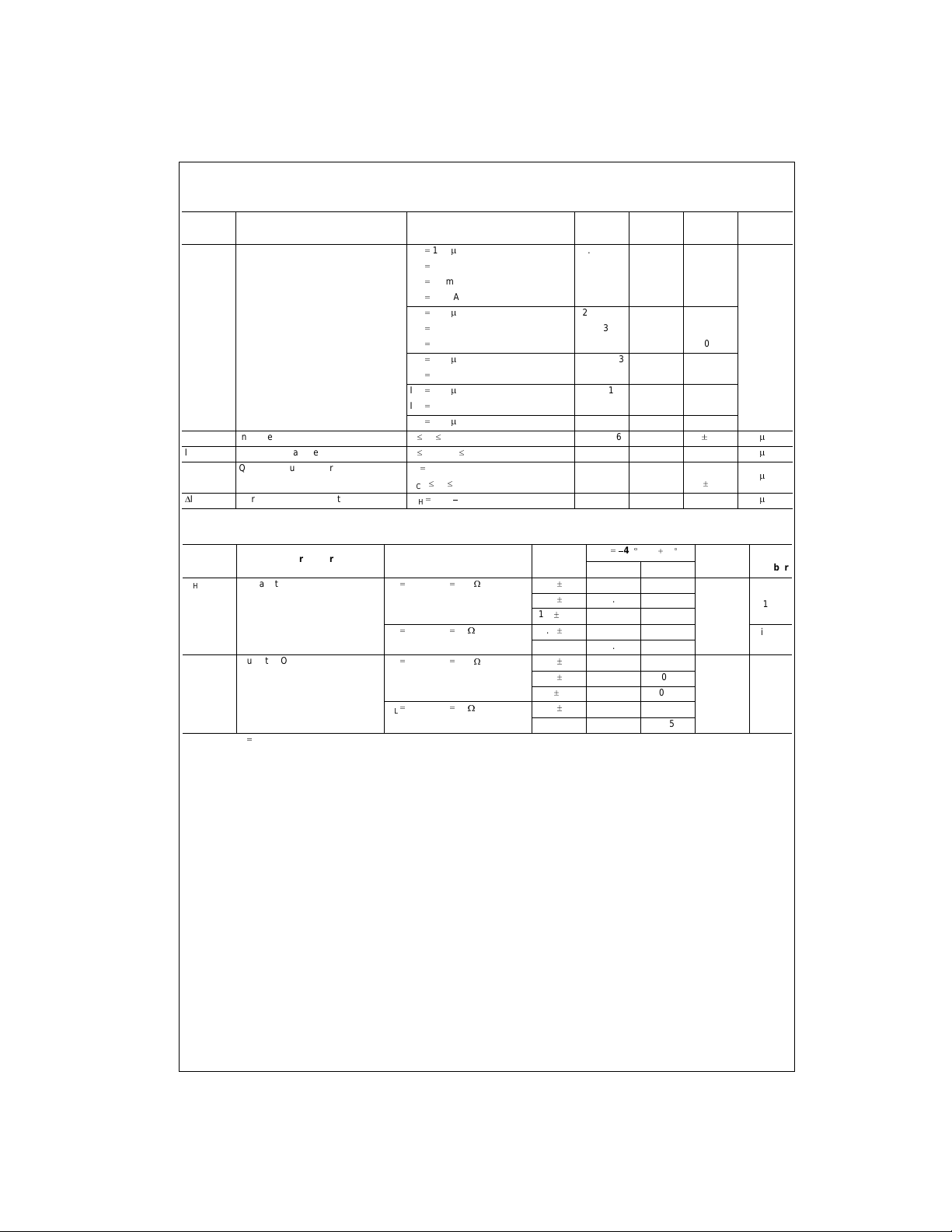
DC Electrical Characteristics (Continued)
V
Symbol Parameter Conditions
74VCX08
V
OL
LOW Level Output Voltage IOL 100 PA 2.7 to 3.6 0.2
12 mA 2.7 0.4
I
OL
I
18 mA 3.0 0.4
OL
(V)
CC
Min Max Units
IOL 24 mA 3.0 0.55
100 PA 2.3 to 2.7 0.2
I
OL
I
12 mA 2.3 0.4
OL
IOL 18 mA 2.3 0.6
100 PA 1.65 to 2.3 0.2
I
OL
I
6 mA 1.65 0.2
OL
IOL 100 PA 1.4 to 1.6 0.2
2 mA 1.4 0.35
I
OL
I
100 PA1.20.05
I
I
I
'
I
OFF
CC
Input Leakage Current 0 d VI d 3.6V 1.2 to 3.6
Power Off Leakage Current 0 d (VI, VO) d 3.6V 0 10
Quiescent Supply Current VI VCC or GND 1.2 to 3.6 20
I
Increase in ICC per Input VIH VCC 0.6V 2.7 to 3.6 750
CC
OL
VCC d VI d 3.6V 1.2 to 3.6
r
5.0
r
20
AC Electrical Characteristics (Note 7)
V
TA 40qC to 85qC
Symbol Parameter Conditions
t
PHL
t
PLH
t
OSHL
t
OSLH
Note 7: For CL pF, add approximately 300 ps to the AC max imum specification.
Note 8: Skew is defined as the absolute value of the difference between t he actual propagat ion delay for any t w o separate outputs of t he same device. The
specification applies to any outputs swi tching in the same direc t ion, either HIGH-to- LOW (t
Propagation Delay CL 30 pF, RL 500
C
15 pF, RL 2k
L
Output to Output Skew CL 30 pF, RL 500
:
:
:
(Note 8) 2.5 r 0.2 0.5
15 pF, RL 2k
C
L
:
CC
(V) Min Max Number
Units
3.3 r 0.3 0.6 2.8
2.5 r 0.2 0.8 3.7
1.8 r 0.15 1.0 7.4
ns
1.5 r 0.1 1.0 14.8
1.2 1.5 37.0
3.3 r 0.3 0.5
1.8 r 0.15 0.75
ns
1.5 r 0.1 1.5
1.2 1.5
) or LOW-to-HIGH (t
OSHL
OSLH
).
V
P
A
P
A
P
A
P
A
Figure
Figures
1, 2
Figures
3, 4
www.fairchildsemi.com 4
 Loading...