Fairchild 74LVX4245 service manual

查询74LVX4245M供应商
74LVX4245
8-Bit Dual Supply Translating Transceiver
with 3-STATE Output s
74LVX4245 8-Bit Dual Supply Translating Transceiver with 3-STATE Outputs
January 1993
Revised September 2003
General Description
The LVX4245 is a dual-supp ly, 8-bit translatin g tran sceiv er
that is designed to interfa ce between a 5V bus and a 3V
bus in a mixed 3V/5V sup ply environment. The Transmit/
Receive (T/R
Transmit (active-HIGH) enables data from A Ports to B
Ports; Receive (ac tive-LOW) enables da ta from B Ports to
A Ports. The Output Enable inpu t, when HIGH, disables
both A and B Port s by placing them in a high impedance
condition. The A Port interfaces with the 5V bus; the B Port
interfaces with the 3V bus.
The LVX4245 is suitable for mixed voltage applications
such as laptop com puters using 3.3V CPU’s and 5V LCD
displays.
) input determines the direc tion of data flow.
Features
■ Bidirectional interface between 5V and 3V buses
■ Control inputs compatible with TTL level
■ 5V data flow at A Port and 3V data flow at B Port
■ Outputs source/sink 24 mA at 5V bus; 12 mA at 3V bus
■ Guaranteed simultaneous switching noise level and
dynamic threshold performan ce
■ Implements patented EMI reduction circuitry
■ Functionally compatible with the 74 series 245
Ordering Code:
Order Number Package Number Package Description
74LVX4245WM M24B 24-Lead Small Outline Integrated Circuit (SOIC), JEDEC MS-013, 0.300" Wide
74LVX4245QSC MQA24 24-Lead Quarter Size Outline Package (QSOP), JEDEC MO-137, 0.150" Wide
74LVX4245MTC MTC24 24-Lead Thin Shrink Small Outline Package (TSSOP), JEDEC MO-153, 4.4mm Wide
Devices also availab l e in Tape and Reel. Specify by appending th e s uffix let t er “X” to the ordering code.
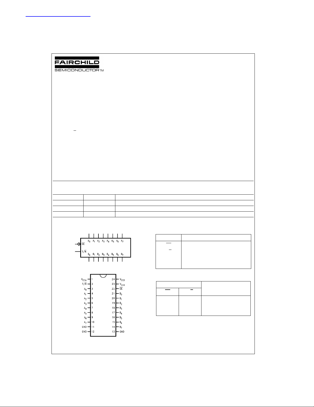
Logic Symbol
Connection Diagram
Pin Descriptions
Pin Names Description
A
B
OE
T/R
0–A7
0–B7
Output Enable Input
Transmit/Receive Input
Side A Inputs or 3-STATE Outpu ts
Side B Inputs or 3-STATE Outpu ts
Truth Table
Inputs Outputs
OE
L L Bus B Data to Bus A
L H Bus A Data to Bus B
H X HIGH-Z State
H = HIGH Voltage Level
L = LOW Voltage Level
X = Immaterial
© 2003 Fairchild Semiconductor Corporation DS011540 www.fairchildsemi.com
T/R

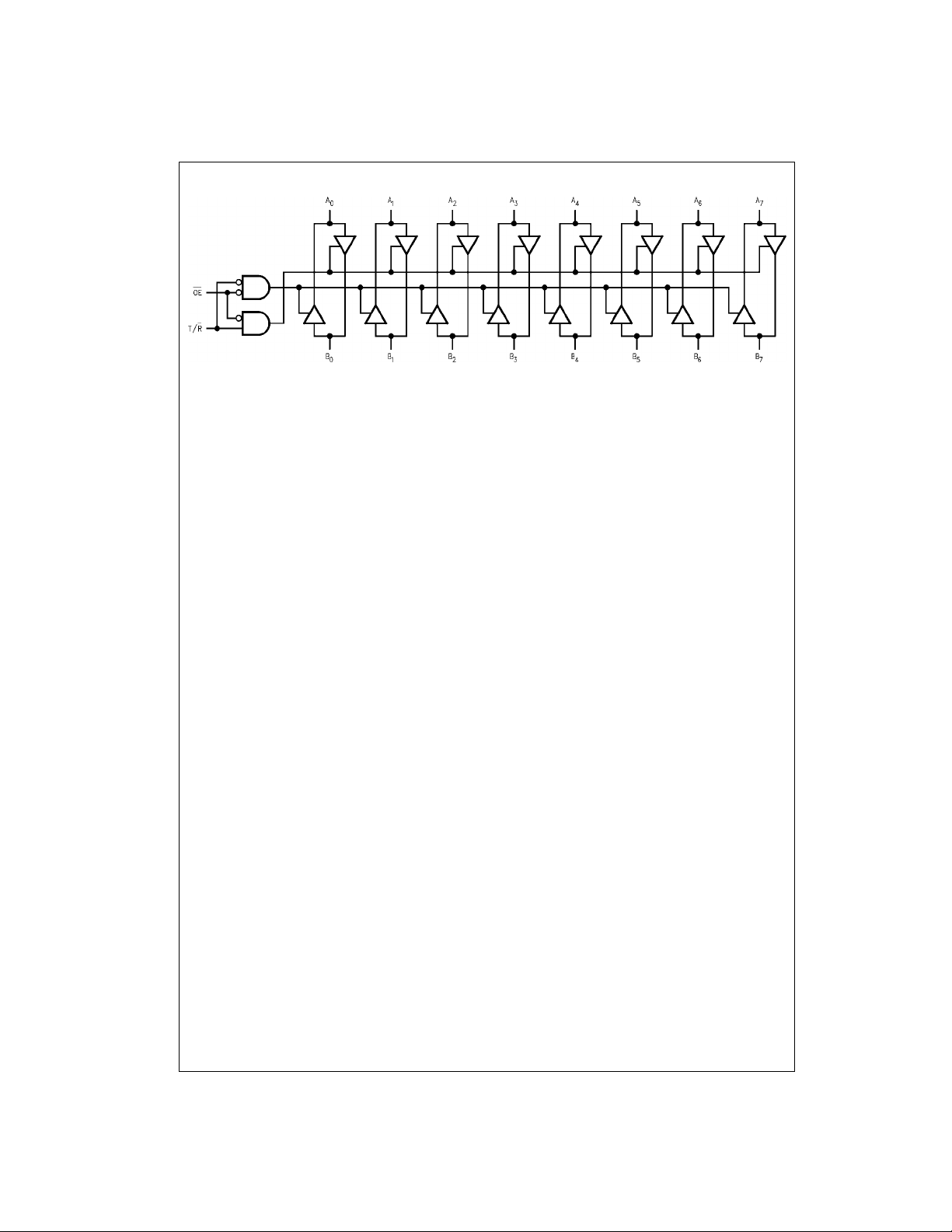
Logic Diagram
74LVX4245
www.fairchildsemi.com 2

Absolute Maximum Ratings(Note 1) Recommended Operating
Supply Voltage (V
DC Input Voltage (V
DC Input/Output Voltage (V
@ A
n
@B
n
DC Input Diode Current (I
, T/R ±20 mA
@ OE
DC Output Diode Current (I
, V
CCA
) −0.5V to +7.0V
CCB
) @ OE, T/R −0.5V to V
I
)
I/O
−0.5V to V
−0.5V to V
)
IN
) ±50 mA
OK
DC Output Source or Sink Current
(I
) ±50 mA
O
DC V
or Ground Current
CC
per Output Pin (I
and Max Current @ I
CC
@ I
or I
) ±50 mA
GND
CCA
CCB
Storage Temperature Range
) −65°C to +150°C
(T
STG
DC Latch-Up Source or
Sink Current
+ 0.5V
CCA
+ 0.5V
CCA
+ 0.5V
CCB
±200 mA
±100 mA
±300 mA
Conditions
Supply Voltage
V
CCA
V
CCB
Input Voltage (V
Input/Output Voltage (V
@ A
n
@ B
n
Free Air Operating Temperature (TA) −40°C to +85°C
Minimum Input Edge Rate (
from 30% to 70% of V
V
IN
VCC @ 3.0V, 4.5V, 5.5V
Note 1: The “Absolute Maximum Ratings” are those value s beyond which
the safety of the d evice cannot b e guaranteed . The device sh ould not be
operated at these limit s. The parametric values defi ned in the Electrical
Characteristics tabl es are not guaranteed at the ab s olute maximum r atings.
The “Recomm ended O peratin g Cond itions ” table will defin e the condition s
for actual device operation.
Note 2: Unused inputs must he held HIGH or LOW. They may not float.
(Note 2)
) @ OE, T/R 0V to V
I
)
I/O
∆t/∆V) 8 ns/V
CC
DC Electrical Characteristics
V
Symbol Parameter
V
Minimum An, T/R, 5.5 3.3 2.0 2.0
IHA
HIGH Level OE 4.5 3.3 2.0 2.0 ≥ VCC − 0.1V
V
Input Voltage B
IHB
V
Maximum An, T/R, 5.5 3.3 0.8 0.8
ILA
LOW Level OE
Input Voltage B
V
ILB
V
Minimum HIGH Level 4.5 3.0 4.5 4.4 4.4
OHA
Output Voltage 4.5 3.0 4.25 3.86 3.76 I
V
OHB
V
Maximum LOW Level 4.5 3.0 0.002 0.1 0.1 V I
OLA
Output Voltage 4.5 3.0 0.18 0.36 0.44 IOL = 24 mA
V
OLB
I
Maximum Input VI = V
IN
Leakage Current 5.5 3.6 ±0.1 ±1.0 µA
@ OE, T/R
I
Maximum 3-STATE VI = VIL, V
OZA
Output Leakage 5.5 3.6 ±0.5 ±5.0 µAOE = V
@ A
I
∆I
OZB
CC
n
Maximum 3-STATE VI = VIL, V
Output Leakage 5.5 3.6 ±0.5 ±5.0 µAOE = V
@ B
n
Maximum I
@ An, T/R, OE
Input @ B
n
n
/Input 5.5 3.6 1.0 1.35 1.5 mA VI = V
CCT
n
CCAVCCB
(V) (V) Typ Guaranteed Limits
5.0 3.6 2.0 2.0
5.0 2.7 2.0 2.0
4.5 3.3 0.8 0.8 ≥ VCC −0.1V
5.0 2.7 0.8 0.8
5.0 3.6 0.8 0.8
4.5 3.0 2.99 2.9 2.9
4.5 3.0 2.8 2.4 2.4 I
4.5 2.7 2.5 2.4 2.4 I
4.5 3.0 0.002 0.1 0.1 I
4.5 3.0 0.1 0.31 0.4 V IOL = 12 mA
4.5 2.7 0.1 0.31 0.4 IOL = 8 mA
5.5 3.6 0.35 0.5 mA VI = V
TA +25°CTA = −40°C to +85°C
Units Conditions
V
V
V
V
V
OUT
V
OUT
I
OUT
= −24 mA
OH
I
OUT
= −12 mA
OH
= −8 mA
OL
OUT
OUT
VO = V
VO = V
= −100 µA
= −100 µA
=100 µA
= 100 µA
4.5V to 5.5V
2.7V to 3.6V
0V to V
0V to V
≤ 0.1V or
≤ 0.1V or
, GND
CCA
IH
CCA
, GND
CCA
IH
CCA
, GND
CCB
− 2.1V
CCA
− 0.6V
CCB
74LVX4245
CCA
CCA
CCB
3 www.fairchildsemi.com
 Loading...