Fairchild 74LVX138 service manual

查询74LVX138供应商
74LVX138
Low Voltage 1-of-8 Decoder/Demultiplexer
74LVX138 Low Voltage 1-of-8 Decoder/Demultiplexer
June 1993
Revised October 2003
General Description
The LVX138 is a high-sp eed 1 -of-8 deco der/de multi plex er.
This device is ideally suited for high-speed bipolar memory
chip select address decoding. The multiple input enables
allow parallel expansion to a 1-of-24 decoder using just
three LVX138 devices or a 1-of-32 decoder using four
LVX138 devices and one inverter.
Features
■ Input voltage level translation from 5V to 3V
■ Ideal for low power/low noise 3.3V applications
■ Guaranteed simultaneous switching noise level and
dynamic threshold performan ce
Ordering Code:
Order Number Package Number Package Description
74LVX138M M16A 16-Lead Small Outline Integrated Circuit (SOIC), JEDEC MS-012, 0.150" Narrow
74LVX138SJ M16D 16-Lead Small Outline Package (SOP), EIAJ TYPE II, 5.3mm Wide
74LVX138MTC MTC16 16-Lead Thin Shrink Small Outline Package (TSSOP), JEDEC MO-153, 4.4mm Wide
Devices also availab l e in Tape and Reel. Specify by appending su ffix let te r “X” to the ordering code .
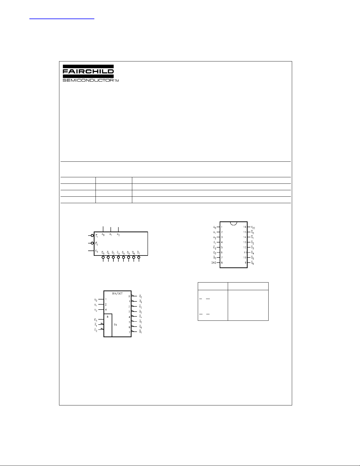
Logic Symbols
Connection Diagram
Pin Descriptions
IEEE/IEC
Pin Names Description
A
E
E
O
0–A2
– E
1
3
0–O7
2
Address Inputs
Enable Inputs
Enable Input
Outputs
© 2003 Fairchild Semiconductor Corporation DS011615 www.fairchildsemi.com

Functional Description
The LVX138 high-speed 1-of-8 decoder/demultiplexer
accepts three binary weighted inputs (A
when enabled, provides eight mutually exclusive active-
74LVX138
LOW outputs (O
inputs, two active-LOW (E
). The LVX138 features three Enable
0–O7
, E2) and one active-HIGH (E3).
1
, A1, A2) and,
0
Truth Table
Inputs Outputs
E
1E2 E3A0A1 A2O0O1O2O3 O4O5O6O7
HXXXXXHHHHHHHH
XHXXXXHHHHHHHH
XXLXXXHHHHHHHH
LLHL LLLHHHHHHH
LLHHL LHLHHHHHH
LLHLHLHHLHHHHH
LLHHHLHHHLHHHH
LLHL LHHHHHLHHH
LLHHLHHHHHHLHH
LLHLHHHHHHHHLH
LLHHHHHHHHHHHL
H = HIGH Voltage Level
L = LOW Voltage Level
X = Immaterial
All outputs will be HIGH unless E
is HIGH.
The LVX138 can be used as an 8-out put demultip lexer by
using one of the a ctive LOW Enable inputs as the data
input and the othe r Enable input s as strobes. The Enable
inputs which are not used must be permanently tied to their
appropriate active-HIGH or active-LOW state.
and E2 are LOW and E
1
3
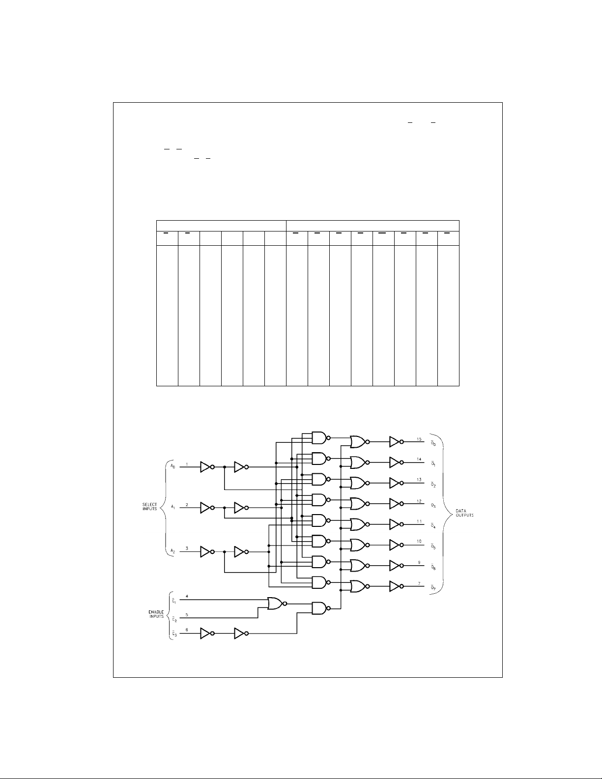
Logic Diagram
Please note that this diagram is provided only for the understanding of logic operations and should not be used to estimate propagation delays.
www.fairchildsemi.com 2

Absolute Maximum Ratings(Note 1) Recommended Operating
Supply Voltage (VCC) −0.5V to +7.0V
DC Input Diode Current (I
V
= −0.5V −20 mA
I
DC Input Voltage (V
DC Output Diode Current (I
V
= −0.5V −20 mA
O
= VCC + 0.5V +20 mA
V
O
DC Output Voltage (V
)
IK
) −0.5V to 7V
I
)
OK
) −0.5V to VCC + 0.5V
O
DC Output Source
or Sink Current (I
DC V
or Ground Current (ICC or I
CC
Storage Temperature (T
) ±25 mA
O
) −65°C to +150°C
STG
) ±75 mA
GND
Power Dissipation 180 mW
Conditions
Supply Voltage (V
Input Voltage (V
Output Voltage (V
Operating Temperature (TA) −40°C to +85°C
Input Rise and Fall Time (
Note 1: The “Absolute Maximum Ratings” are those value s beyond which
the safety of the d evice cannot b e guaranteed . The device sh ould not be
operated at these limit s. The parametric values defi ned in the Electrical
Characteristics tabl es are not guaranteed at the ab s olute maximum r atings.
The “Recomm ended O peratin g Cond itions ” table will defin e the condition s
for actual device operation.
Note 2: Unused inputs must be held HIGH or LOW. They may not float.
(Note 2)
) 2.0V to 3.6V
CC
) 0V to 5.5V
I
)0V to V
O
∆t/∆V) 0 ns/V to 100 ns/V
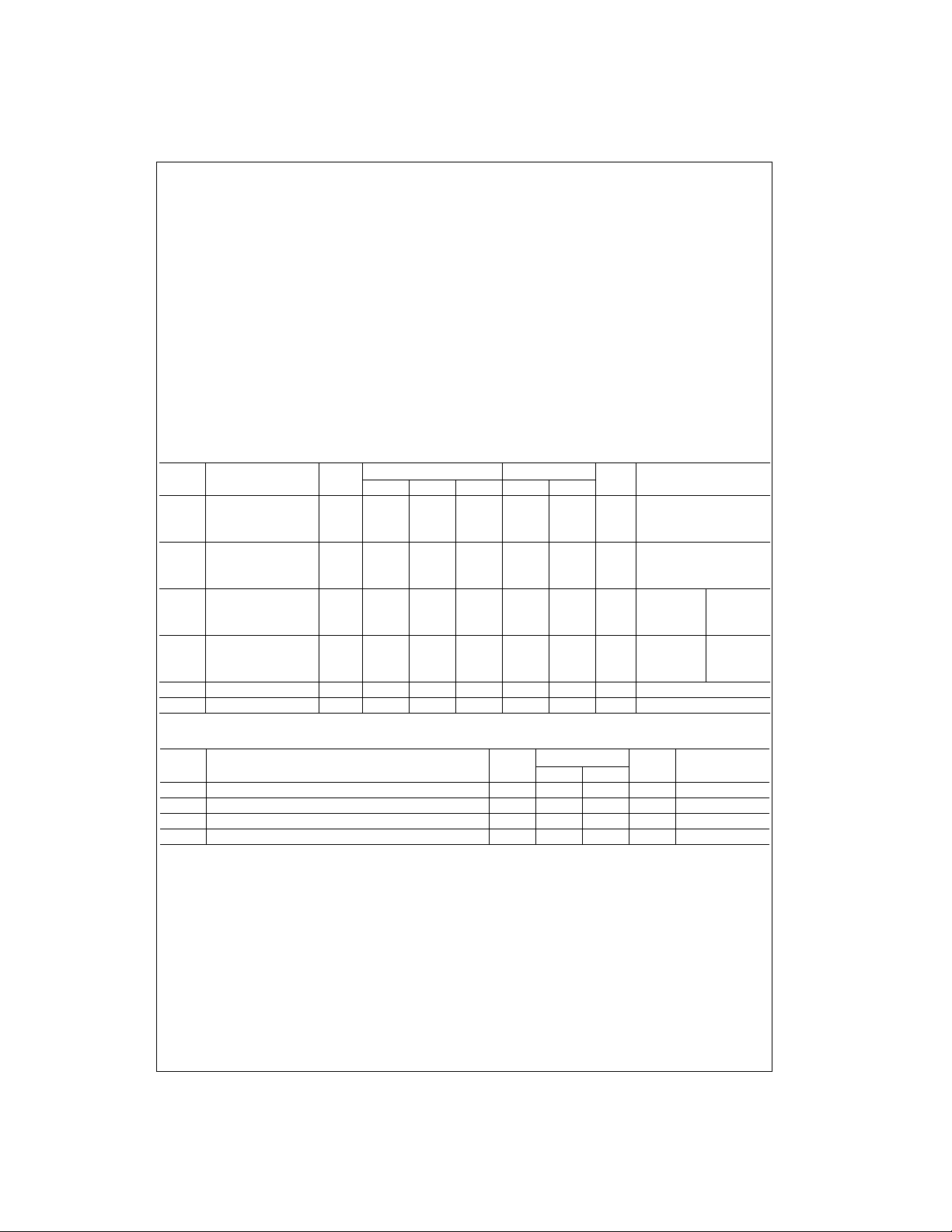
DC Electrical Characteristics
Symbol Parameter
V
HIGH Level 2.0 1.5 1.5
IH
Input Voltage 3.0 2.0 2.0 V
V
LOW Level 2.0 0.5 0.5
IL
Input Voltage 3.0 0.8 0.8 V
V
HIGH Level 2.0 1.9 2.0 1.9 VIN = VIL or VIHIOH = −50 µA
OH
Output Voltage 3.0 2.9 3.0 2.9 V IOH = −50 µA
V
LOW Level 2.0 0.0 0.1 0.1 VIN = VIL or VIHIOL = 50 µA
OL
Output Voltage 3.0 0.0 0.1 0.1 V IOL = 50 µA
I
Input Leakage Current 3.6 ±0.1 ±1.0 µAVIN = 5.5V or GND
IN
I
Quiescent Supply Current 3.6 4.0 40.0 µAVIN = VCC or GND
CC
V
CC
3.6 2.4 2.4
3.6 0.8 0.8
3.0 2.58 2.48 IOH = −4 mA
3.0 0.36 0.44 IOL = 4 mA
TA = +25°CT
Min Typ Max Min Max
= −40°C to +85°C
A
Units Conditions
74LVX138
CC
Noise Characteristics
Symbol Parameter
V
Quiet Output Maximum Dynamic V
OLP
V
Quiet Output Minimum Dynamic V
OLV
V
Minimum HIGH Level Dynamic Input Voltage 3.3 2.0 V 50
IHD
V
Maximum LOW Level Dynamic Input Voltage 3.3 0.8 V 50
ILD
Note 3: Input tr = tf = 3 ns
(Note 3)
OL
OL
V
CC
(V) Typ Limit
3.3 0.3 0.5 V 50
3.3 −0.3 −0.5 V 50
TA = 25°C
3 www.fairchildsemi.com
Units
(pF)
C
L
 Loading...