Fairchild 74LVT574 service manual

74LVT574 • 74LVTH574
Low Voltage Octal D-Type Flip-Flop
with 3-STATE Outputs
74LVT574 • 74LVTH574 Low Voltage Octal D-Type Flip-Flop with 3-STATE Outputs
March 1999
Revised March 2005
General Description
The LVT574 and LVTH574 are high-speed, low-power
octal D-type flip-flop featur ing separate D-type inputs for
each flip-flop and 3-STATE outputs for bus-oriented applications. A buffered Clock (CP) and Output Enable (OE
common to all flip-flops.
The LVTH574 data inputs include bushold, eliminati ng the
need for external pull-up resistors to hold unused inputs.
These octal flip-flops are d esigned for low-voltage (3.3V)
V
applications, but with the capability to provide a TTL
CC
interface to a 5V environme nt. The LVT574 and LVTH574
are fabricated with an advanced BiCMOS technology to
achieve high speed operation similar to 5V ABT while
maintaining a low power dissipation.
Features
■ Input and output interface capability to systems at
5V V
CC
■ Bushold data inputs eliminate the need for external
) are
pull-up resistors to hold unused inputs (74LVTH574),
also available without bushold feat ure (74LVT574)
■ Live insertion/extraction per mi tt ed
■ Power Up/Down high impedance provides glitch-free
bus loading
■ Outputs source/sink
■ Functionally compatible with the 74 series 574
■ Latch-up performance exce eds 500 mA
■ ESD performance:
Human-body model
Machine model ! 200V
Charged-device model
32 mA/64 mA
!
2000V
!
1000V
Ordering Code:
Order Number
74LVT574WM M20B 20-Lead Small Outline Integrated Circuit (SOIC), JEDEC MS-013, 0.300" Wide
74LVT574SJ M20D Pb-Free 20-Lead Small Outline Package (SOP), EIAJ TYPE II, 5.3mm Wide
74LVT574MSA MSA20 20-Lead Shrink Small Outline Package (SSOP), JEDEC MO-150, 5.3mm Wide
74LVT574MTC MTC20 20-Lead Thin Shrink Small Outline Package (TSSOP), JEDEC MO-153, 4.4mm Wide
74LVT574MTCX_NL
(Note 1)
74LVTH574WM M20B 20-Lead Small Outline Integrated Circuit (SOIC), JEDEC MS-013, 0.300" Wide
74LVTH574SJ M20D Pb-Free 20-Lead Small Outline Package (SOP), EIAJ TYPE II, 5.3mm Wide
74LVTH574MSA MSA20 20-Lead Shrink Small Outline Package (SSOP), JEDEC MO-150, 5.3mm Wide
74LVTH574MTC MTC20 20-Lead Thin Shrink Small Outline Package (TSSOP), JEDEC MO-153, 4.4mm Wide
74LVTH574MTCX_NL
(Note 1)
Device also availab le in Tape and Reel. Specify by appending suffix let te r “X” to the ordering code .
Pb-Free package per JEDEC J-STD-020B.
Note 1: “_NL” indicates Pb-Free pac k age (per JEDEC J-S T D -020B). Device available in Tape and Reel only.
Package
Number
MTC20 Pb-Free 20-Lead Thin Shrink Small Outline Package (TSSOP), JEDEC MO-153, 4.4mm
Wide
MTC20 Pb-Free 20-Lead Thin Shrink Small Outline Package (TSSOP), JEDEC MO-153, 4.4mm
Wide
Package Description
© 2005 Fairchild Semiconductor Corporation DS012451 www.fairchildsemi.com

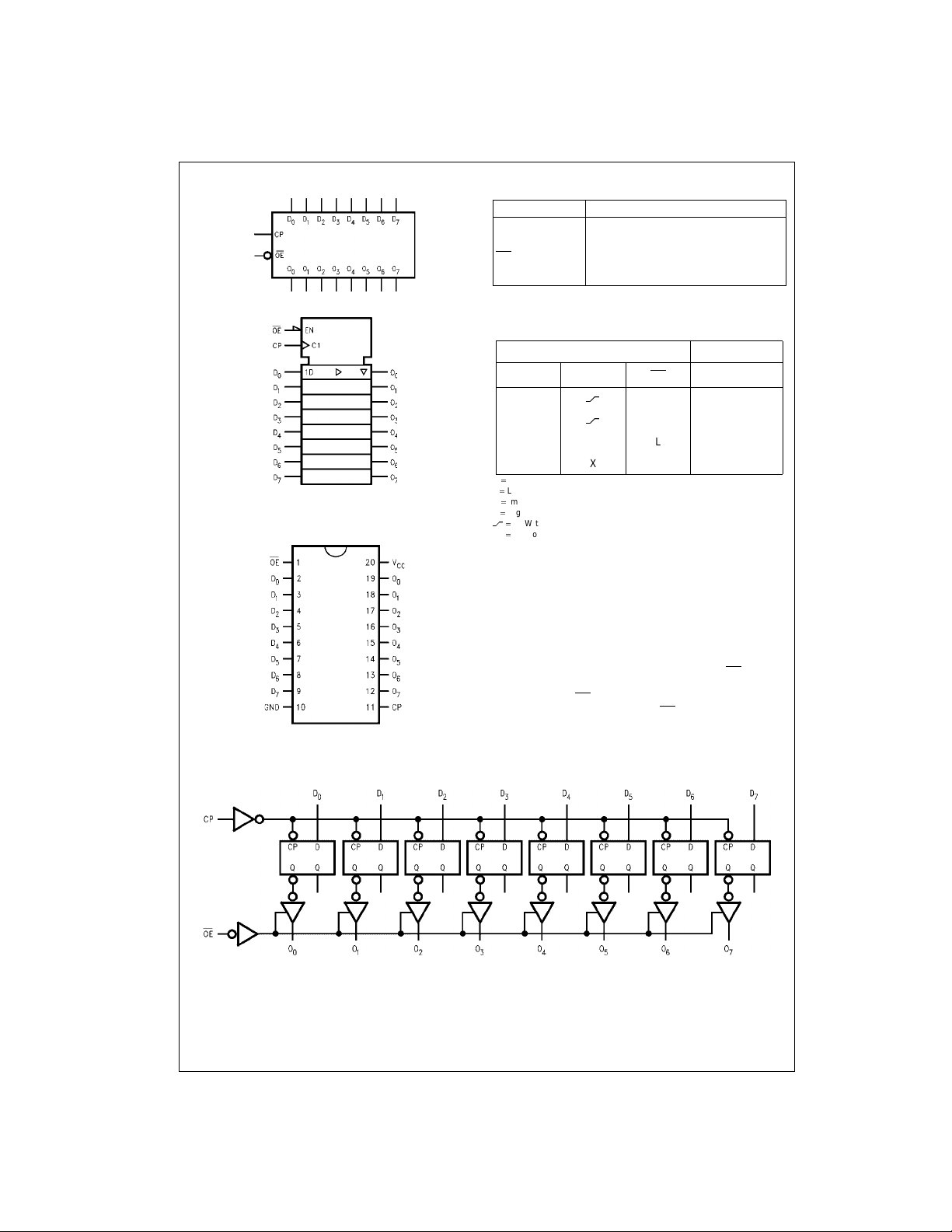
Logic Symbols
Pin Descriptions
Pin Names Description
D
0–D7
CP Clock Pulse Input
OE
O
0–O7
Data Inputs
3-STATE Output Enable Input
3-STATE Outputs
74LVT574 • 74LVTH574
Connection Diagram
IEEE/IEC
Truth Table
Inputs Outputs
D
n
H
L
XLL O
CP OE O
LH
LL
n
o
XXH Z
H HIGH Voltage Level
LOW Voltage Level
L
X
Immaterial
Z
High Impedance
LOW-to-HIGH Transition
O
Previous Oo before HIGH to LOW of CP
o
Functional Description
The LVT574 and LVTH574 consist of eig ht edge-trig gered
flip-flops with individual D-type inputs and 3-STATE true
outputs. The buffered clock and buffered Output Enable
are common to all flip-flops. The eight flip-flops will store
the state of their individual D-type inputs that meet the
setup and hold time requirements on the LOW-to-HIGH
Clock (CP) transition . With the Output Enable (OE
the contents of the eight fl ip-flops are ava ilable at the o utputs. When the OE
impedance state. Operation of the OE
is HIGH, the outputs go to the high
input does not affect
the state of the flip-flops.
) LOW,
Logic Diagram
Please note that this diagram is provided only for the understanding of logic operations and should not be used to estimate propagation delays.
www.fairchildsemi.com 2

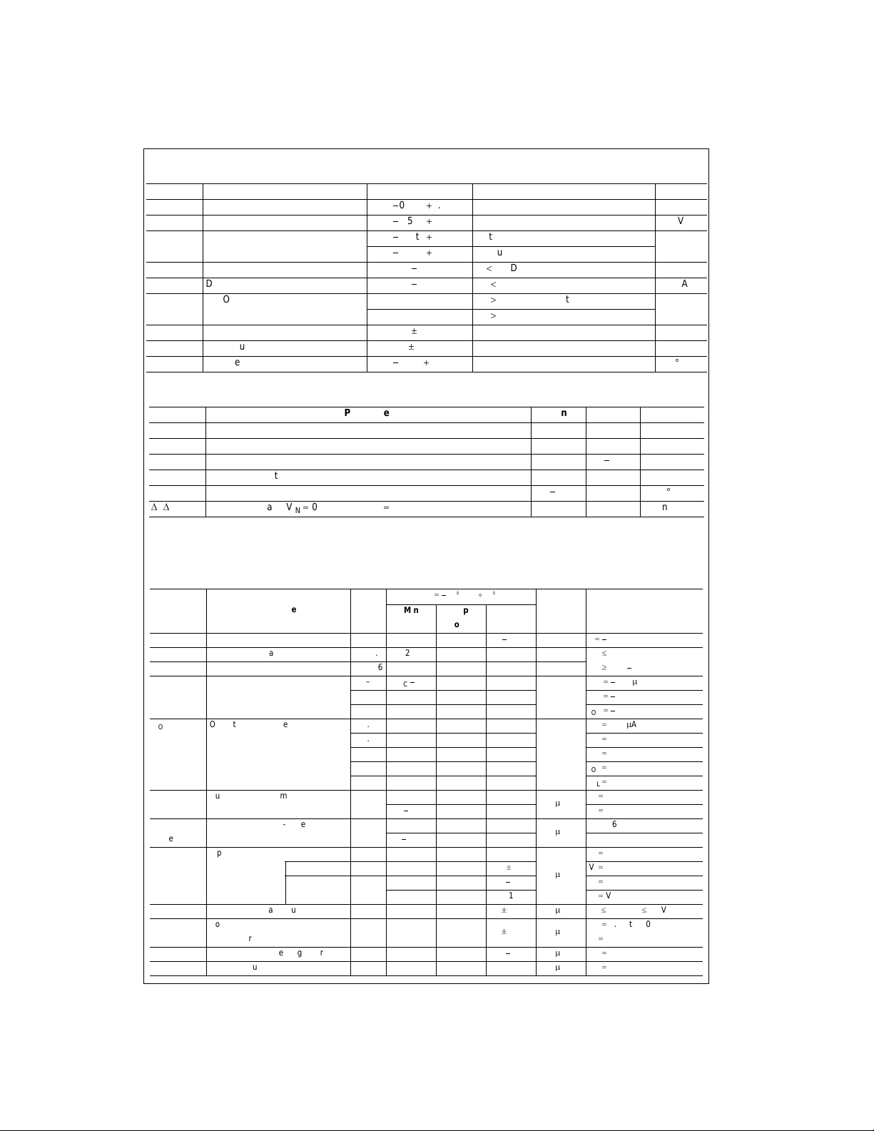
Absolute Maximum Ratings(Note 2)
Symbol Parameter Value Conditions Units
V
V
V
I
IK
I
OK
I
O
I
CC
I
GND
T
CC
I
O
STG
Supply Voltage
DC Input Voltage
DC Output Voltage
DC Input Diode Current
DC Output Diode Current
DC Output Current 64 VO ! VCCOutput at HIGH State
DC Supply Current per Supply Pin
DC Ground Current per Ground Pin
Storage T emperature
0.5 to 4.6 V
0.5 to 7.0 V
0.5 to 7.0 Output in 3-STATE
0.5 to 7.0 Outp ut in HIGH or LOW State (Note 3)
50 VI GND mA
50 VO GND mA
128 V
r
64 mA
r
128 mA
65 to 150
! VCCOutput at LOW State
O
mA
Recommended Operating Conditions
Symbol Parameter Min Max Units
V
CC
V
I
I
OH
I
OL
T
A
't/'
Note 2: Absolute Maximum continuous ratings are those values beyond which damage to the device may occur. Exposure to these conditions or conditions
beyond those indica te d m ay adversely affect de v ic e reliability. Functional operation under absolute maxi m um rated conditions is no t implied.
Note 3: I
Supply Voltage 2.7 3.6 V
Input Voltage 0 5.5 V
HIGH-Level Output Current
32 mA
LOW-Level Output Current 64 mA
Free-Air Operating Temperature
40 85
q
C
V Input Edge Rate, VIN 0.8V–2.0V, VCC 3.0V 0 10 ns/V
Absolute Maximum Rating must be observed.
O
74LVT574 • 74LVTH574
V
q
C
DC Electrical Characteristics
Symbol Parameter
V
IK
V
IH
V
IL
V
OH
V
OL
I
I(HOLD)
(Note 5)
I
I(OD)
(Note 5) Current to Change State
I
I
I
OFF
I
PU/PD
I
OZL
I
OZH
Input Clamp Diode Voltage 2.7
Input HIGH Voltage 2.7–3.6 2.0 V VO d 0.1V or
Input LOW Voltage 2.7–3.6 0.8 V VO t VCC 0.1V
Output HIGH Voltage 2.7–3.6 VCC 0.2
Output LOW Voltage 2.7 0.2
Bushold Input Minimum Drive 3.0 75
Bushold Input Over-Drive 3.0 500
Input Current 3.6 10
Power Off Leakage Current 0
Power Up/Down 3-ST ATE
Output Current VI GND or V
3-STATE Output Leakage Current 3.6
3-STATE Output Leakage Current 3.6 5
Control Pins 3.6
Data Pins 3.6
0–1.5V
V
CC
(V)
2.7 2.4 IOH 8 mA
3.0 2.0 I
2.7 0.5 IOL 24 mA
3.0 0.4 IOL 16 mA
3.0 0.5 IOL 32 mA
3.0 0.55 IOL 64 mA
T A 40qC to 85qC
Min Typ Max
(Note 4)
75 VI 2.0V
500 (Note 7)
r
r
100
r
100
Units Conditions
1.2 V II 18 mA
IOH 100 PA
V
OH
IOL 100 PA
V
VI 0.8V
P
A
(Note 6)
P
A
1V
5V
1V
5
VI 5.5V
0V or V
I
P
A
0V
I
V
I
P
A0V d VI or VO d 5.5V
VO 0.5V to 3.0V
P
A
P
AVO 0.5V
P
AVO 3.0V
32 mA
CC
CC
CC
3 www.fairchildsemi.com
 Loading...