

Fairchild 74LVT16374 service manual

74LVT16374 • 74LVTH16374
Low Voltage 16-Bit D-Type Flip-Flop
with 3-STAT E Outputs
74LVT16374 • 74LVTH16374 Low Voltage 16-Bit D-Type Flip-Flop with 3-STATE Outputs
January 1999
Revised June 2005
General Description
The LVT16374 and LVTH16374 contain sixteen non-inverting D-type flip-flops with 3-STATE outputs and is intended
for bus oriented applications. The device is byte controlled.
A buffered clock (CP) and Output Ena ble (OE
mon to each byte and can be shorted together for full 16-bit
operation.
The LVTH16374 data inputs include bushold, elim inating
the need for external pull-up resistors to hold unused
inputs.
These flip-flops are designed for low-voltage (3.3V) V
applications, but with the capability to provide a TTL inter-
face to a 5V environment. Th e LVT16374 and LVTH16374
are fabricated with an advanced BiCMOS technology to
achieve high speed operation similar to 5V ABT while
maintaining a low power dissipation.
) are com-
Features
■ Input and output interface capability to systems at
5V V
CC
■ Bushold data inputs eliminate the need for external
pull-up resistors to hold unus ed inputs (74LVTH16374),
also available without bushold feat ure (74LVT16374)
■ Live insertion/extraction per mi tt ed
■ Power Up/Power Down high impedance provides
glitch-free bus loading
■ Outputs source/sink
CC
■ Functionally compatible with the 74 series 16374
■ Latch-up performance exce eds 500 mA
■ ESD performance:
Human-body model
Machine model
Charged-device model
■ Also packaged in plastic Fine-Pitch Ball Grid Array
(FBGA)
!
200V
!
Ordering Code:
Order Number Package Number Package Descript io n
74LVT16374G
(Note 1)(Note 2)
74LVT16374MEA
(Note 2)
74LVT16374MTD
(Note 2)
74LVTH16374G
(Note 1)(Note 2)
74LVTH16374MEA
(Note 2)
74LVTH16374MTD
(Note 2)
Note 1: Ordering code “G” indicates Trays.
Note 2: Device also available in Tape and Reel. Specify by appending suffix letter “X” to the ordering code.
BGA54A
(Preliminary)
MS48A 48-Lead Small Shrink Outline Package (SSOP), JEDEC MO-118, 0.300" Wide
MTD48 48-Lead Thin Shrink Small Outline Package (TSSOP), JEDEC MO-153, 6.1mm Wide
BGA54A 54-Ball Fine-Pitch Ball Grid Array (FBGA), JEDEC MO-205, 5.5mm Wide
MS48A 48-Lead Small Shrink Outline Package (SSOP), JEDEC MO-118, 0.300" Wide
MTD48 48-Lead Thin Shrink Small Outline Package (TSSOP), JEDEC MO-153, 6.1mm Wide
54-Ball Fine-Pitch Ball Grid Array (FBGA), JEDEC MO-205, 5.5mm Wide
32 mA/64 mA
2000V
!
1000V
Logic Symbol
© 2005 Fairchild Semiconductor Corporation DS012022 www.fairchildsemi.com
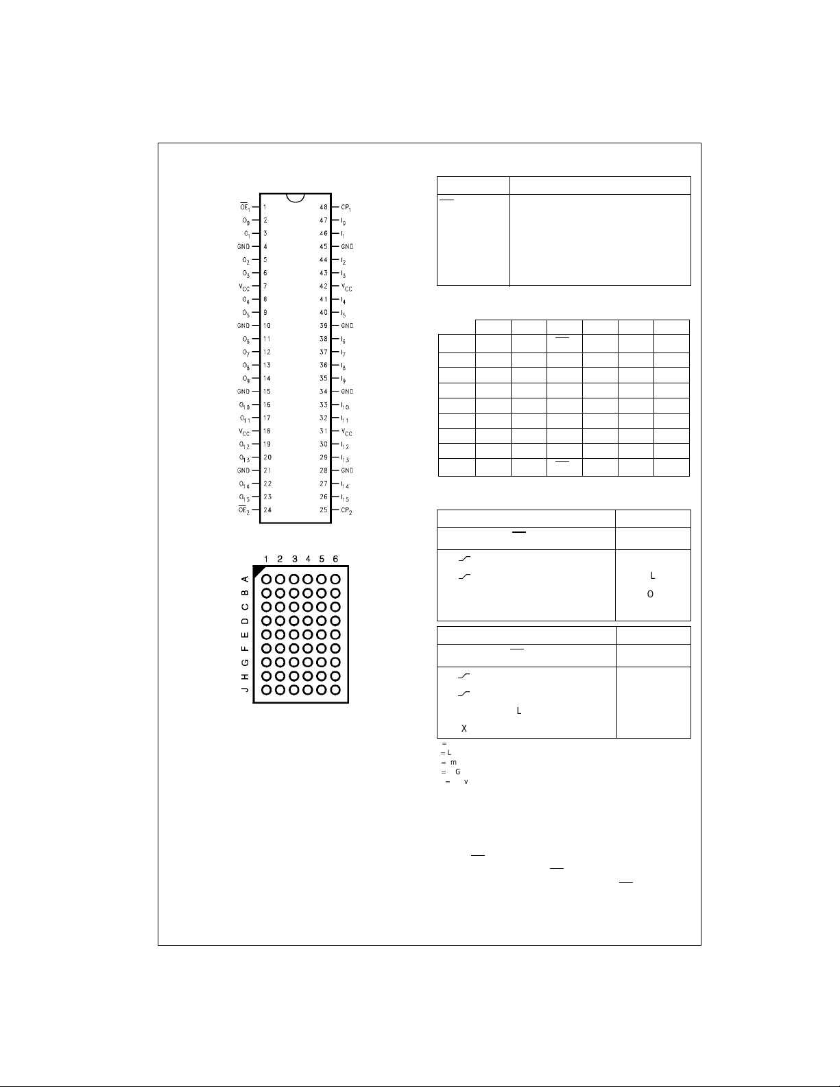
Connection Diagrams
Pin Descriptions
Pin Assignment for SSOP and TSSOP
74LVT16374 • 74LVTH16374
Pin Assignment for FBGA
Pin Names Description
OE
CP
I
0–I15
O
0–O15
n
n
Output Enable Input (Active LOW)
Clock Pulse Input
Inputs
3-STATE Outputs
NC No Connect
FBGA Pin Assignments
123456
A O
B O
C O
D O
E O
F O
G O
H O
J O
NC OE1CP1NC I
0
O1NC NC I
2
O3V
4
6
8
10
12O11VCCVCCI11
14O13
15
CCVCCI3
O5GND GND I
O7GND GND I
O9GND GND I
NC NC I
NC OE2CP2NC I
1
5
7
9
13I14
Truth Tables
Inputs Outputs
CP
1
OE
1
LH H
LL L
LL X O
XH X Z
I0–I
7
O0–O
0
I
2
I
4
I
6
I
8
I
10
I
12
15
7
o
(Top Thru View)
Functional Description
The LVT16374 and LVTH16374 consist of sixteen
edge-triggered flip-flops with individual D-type inputs and
3-STATE true outputs. The device is byte controlled with
each byte functioning identically, but independent of the
other. The control pins can be sho rted together to obtain
full 16-bit operati on. Each byte has a buffered clock and
buffered Output Enable common to all flip-flops within that
byte. The description which follows applies to each byte.
www.fairchildsemi.com 2
Inputs Outputs
CP
OE
2
2
LH H
LL L
LL X O
I8–I
15
O8–O
15
o
XH X Z
H HIGH Voltage Level
LOW Voltage Level
L
X
Immaterial
HIGH Impedance
Z
Previous Oo before HIGH to LOW of CP
O
o
Each flip-flop will store the state of the ir individual D-type
inputs that meet the set up and hold tim e requirements on
the LOW-to-HIGH Clock (CP
Enable (OE
) LOW, the contents of the flip-flops are avail-
n
able at the outputs. When OE
the high impedance state. Ope ration of the OE
) transition. With the Out put
n
is HIGH, the outputs go to
n
input does
n
not affect the state of the flip-flops.
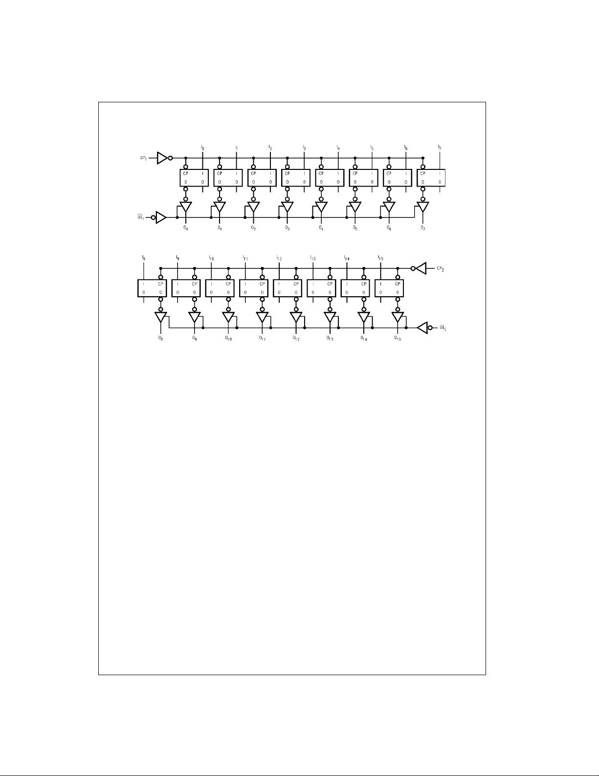
Logic Diagrams
Byte 1 (0:7)
Byte 2 (8:15)
Please note that thes e diagrams are provided for the understand ing of logic operation and should not be used to es t im at e propagation delays.
74LVT16374 • 74LVTH16374
3 www.fairchildsemi.com
 Loading...