74LVQ374
Low Voltage Octal D-Type Flip-Flop
with 3-STAT E Outputs
74LVQ374 Low Voltage Octal D-Type Flip-Flop with 3-STATE Outputs
February 1992
Revised June 2001
General Description
The LVQ374 is a high-speed, low-power octal D-type flipflop featuring separ ate D-type inp uts for each flip-flop and
3-STATE outputs for bus-oriented applications. A buffered
Clock (CP) and Output Enabl e (OE
flops.
) are common to all flip-
Features
■ Ideal for low power/low noise 3.3V applications
■ Implements patented EMI reduction circuitry
■ Available in SOIC JEDEC, SOIC EIAJ a nd QS OP pack-
ages
■ Guaranteed simultaneous switching noise level and
dynamic threshold performan ce
■ Improved latch-up immunity
■ Guaranteed incident wave switching into 75
■ 4 kV minimum ESD immunity
■ Buffered positive edge-triggered cl ock
■ 3-STATE outputs drive bus lines or buffer memory
address registers
Ω
Ordering Code:
Order Number Package Number Package Description
74LVQ374SC M20B 20-Lead Small Outline Integrated Circuit (SOIC), JEDEC MS-013, 0.300" Wide
74LVQ374SJ M20D 20-Lead Small Outline Package (SOP), EIAJ TYPE II, 5.3mm Wide
74LVQ374QSC MQA20 20-Lead Quarter Size Outline Package (QSOP), JEDEC MO-137, 0.150" Wide
Devices also availab l e in Tape and Reel. Specify by appending su ffix let te r “X” to the ordering code .
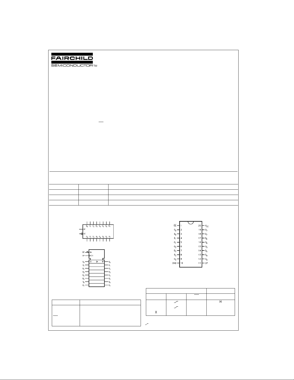
Logic Symbols
Connection Diagram
IEEE/IEC
Truth Table
Pin Descriptions
Pin Names Descriptio n
D
0–D7
CP Clock Pulse Input
OE 3-STATE Output Enable Input
O
0–O7
© 2001 Fairchild Semiconductor Corporation DS011360 www.fairchildsemi.com
Data Inputs
3-STATE Outputs
D
n
H
L
XXH Z
H = HIGH Voltage Level L = LOW Voltage Level
X = Immaterial Z = High Impedance
= LOW-to-HIGH Transition
Inputs Outputs
CP OE O
LH
LL
n

Functional Description
The LVQ374 consists of eight ed ge -tri g ge red fli p -flo ps w ith
individual D-type inputs and 3-STATE true outputs. The
buffered clock and buffered Outp ut Enable ar e common to
74LVQ374
all flip-flops. The eight flip-flops will store the state of their
individual D-type i nputs that meet the setup and hol d time
requirements on the LOW-to-HIGH Clock (CP) transition.
With the Output Enable (OE
eight flip-flops are available at the outputs. When the OE
HIGH, the outputs go to the h igh imped ance state. O peration of the OE
flops.
input does not affect the state of the flip-
) LOW, the contents of the
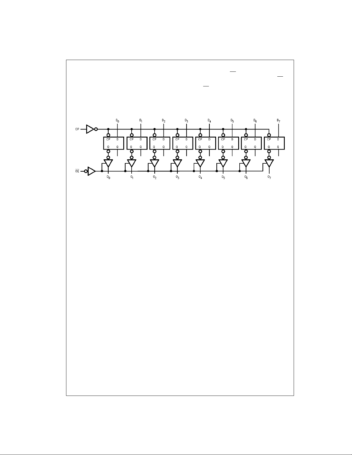
Logic Diagram
Please note that this diagram is provided only for the understanding of logic operations and should not be used to estimate propagation delays.
is
www.fairchildsemi.com 2

Absolute Maximum Ratings(Note 1) Recommended Operating
Supply Voltage (VCC) −0.5V to +7.0V
DC Input Diode Current (I
V
= −0.5V −20 mA
I
= VCC + 0.5V +20 mA
V
I
DC Input Voltage (V
DC Output Diode Current (I
= −0.5V −20 mA
V
O
V
= VCC + 0.5V +20 mA
O
DC Output Voltage (V
)
IK
) −0.5V to VCC + 0.5V
I
)
OK
) −0.5V to VCC + 0.5V
O
DC Output Source
or Sink Current (I
DC V
or Ground Current
CC
or I
(I
CC
GND
Storage Temperature (T
) ±50 mA
O
) ±400 mA
) −65°C to +150°C
STG
DC Latch-Up Source or
Sink Current ±300 mA
Conditions
Supply Voltage (V
Input Voltage (V
Output Voltage (VO)0V to V
Operating Temperature (TA) −40°C to +85°C
Minimum Input Edge Rate (
V
from 0.8V to 2.0V
IN
@ 3.0V 125 mV/ns
V
CC
Note 1: The “Absolute Maximum Ratings” are those value s beyond which
the safety of the d evice cannot b e guaranteed . The device sh ould not be
operated at these limit s. The parametric values defi ned in the Electrical
Characteristics tables are not gu aranteed at the absolute m ax imum ratings .
The “Recomm ended O peratin g Cond itions ” table will defin e the condition s
for actual device operation.
Note 2: Unused inputs must be held HIGH or LOW. They may not float.
(Note 2)
) 2.0V to 3.6V
CC
)0V to V
I
∆V/∆t)
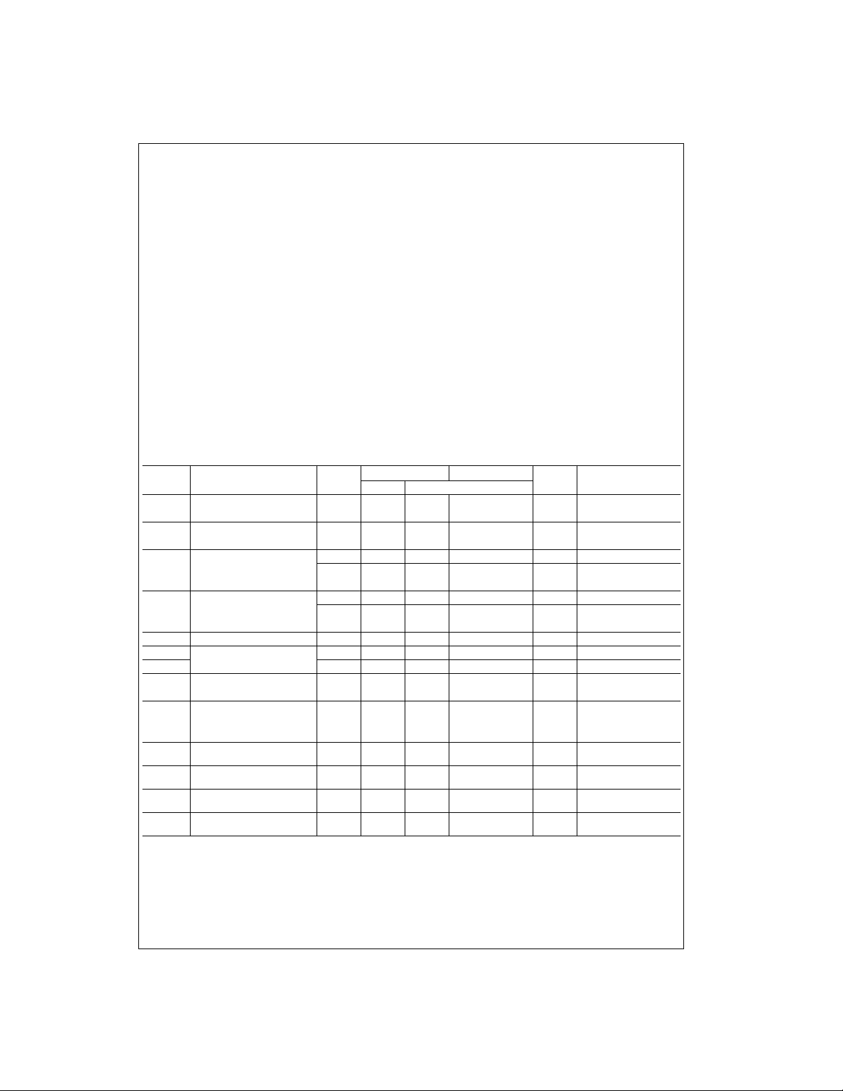
DC Electrical Characteristics
V
Symbol Parameter
V
IH
V
IL
V
OH
V
OL
I
IN
I
OLD
I
OHD
I
CC
I
OZ
V
OLP
V
OLV
V
IHD
V
ILD
Note 3: All outputs loaded; thres holds on input associated with output unde r te s t .
Note 4: Maximum test duration 2.0 ms, one output loaded at a time.
Note 5: Incident wave switching on transmission lines with impedances as low as 75Ω for commercial temperature range is guaranteed for 74LVQ.
Note 6: Worst case package.
Note 7: Max number of outputs def ined as (n). Data inputs are driven 0V to 3.3V; one ou tp ut at GN D .
Note 8: Max number of Data Inputs (n) switching. (n − 1) inputs switching 0V to 3.3 V. Input-under-test s witchin g: 3.3V to thres hold (V
(V
Minimum High Level
Input Voltage or VCC − 0.1V
Maximum Low Level
Input Voltage or VCC − 0.1V
Minimum High Level 3.0 2.99 2.9 2.9 V I
Output Voltage
Maximum Low Level 3.0 0.002 0.1 0.1 V I
Output Voltage
Maximum Input Leakage Current 3.6 ±0.1 ±1.0 µAVI = VCC, GND
Minimum Dynamic 3.6 36 mA V
Output Current (Note 4) 3.6 −25 mA V
Maximum Quiescent
Supply Current or GND
Maximum 3-STATE VI (OE) = VIL, V
Leakage Current 3.6 ±0.25 ±2.5 µAVI = VCC, GND
Quiet Output
), f = 1 MHz.
IHD
Maximum Dynamic V
Quiet Output
Minimum Dynamic V
Maximum High Level
Dynamic Input Voltage
Maximum Low Level
Dynamic Input Voltage
OL
OL
CC
(V) Typ Guaranteed Limits
3.0 1.5 2.0 2.0 V
3.0 1.5 0.8 0.8 V
3.0 2.58 2.48 V
3.0 0.36 0.44 V
3.6 4.0 40.0 µA
3.3 0.5 0.8 V (Note 6)(Note 7)
3.3 −0.3 −0.8 V (Note 6)(Note 7)
3.3 1.7 2.0 V (Note 6)(Note 8)
3.3 1.6 0.8 V (Note 6)(Note 8)
TA = +25°CTA = −40°C to +85°C
Units Conditions
V
= 0.1V
OUT
V
= 0.1V
OUT
= −50 µA
OUT
= VIL or VIH (Note 3)
V
IN
IOH = −12 mA
= 50 µA
OUT
= VIL or VIH (Note 3)
V
IN
IOL = 12 mA
= 0.8V Max (Note 5)
OLD
= 2.0V Min (Note 5)
OHD
VIN = VCC
VO = VCC, GND
), 0V to threshold
ILD
74LVQ374
CC
CC
IH
3 www.fairchildsemi.com
 Loading...