

Fairchild 74LCX241 service manual
查询74LCX241供应商
74LCX241
Low Voltage Octal Buffer/Line Driv er with
5V Tolerant Inputs and Outputs
74LCX241 Low Voltage Octal Buffer/Line Driver with 5V Tolerant Inputs and Outputs
August 1998
Revised March 2005
General Description
The LCX241 is an octal buffer and line drive r designed to
be employed as a mem ory add re ss dr iv er, clock driver a nd
bus oriented transmitter or receiver. The device is designed
for low voltage (2. 5V or 3.3V) V
bility of interfacing to a 5V signal environment.
The LCX241 is fabrica ted with an advanced CMOS tech-
nology to achieve high speed operation whil e maintaining
CMOS low power dissipation.
applications with c apa-
CC
Features
■ 5V tolerant inputs and outputs
■ 2.3V – 3.6V V
■ 6.5 ns t
■ Power-down high impedance inputs and outputs
■ Supports live insertion/withdrawal (Note 1)
■ Implements patented noise/EMI reduction circuitry
■ Latch-up performance exce eds 500 mA
■ ESD performance:
Human Body Model ! 2000V
Machine Model
Note 1: To ensure the high-impedance state during power up or down, OE
should be tied to VCC and OE should be t ied to GND through a resistor: the
minimum value or th e resisto r is dete rmined by the cu rrent-sou rcing c apability of the driver.
specifications provided
CC
max (VCC 3.3V), 10 PA ICC max
PD
!
200V
Ordering Code:
Order Number Package Number Package Description
74LCX241WM M20B 20-Lead Small Outline Integrated Circuit (SOIC), JEDEC MS-013, 0.300" Wide
74LCX241SJ M20D Pb-Free 20-Lead Small Outline Package (SOP), EIAJ TYPE II, 5.3mm Wide
74LCX241MSA MSA20 20-Lead Shrink Small Outline Package (SSOP), JEDEC MO-150, 5.3mm Wide
74LCX241MTC MTC20 20-Lead Thin Shrink Small Outline Package (TSSOP), JEDEC MO-153, 4.4mm Wide
Devices also availab l e in Tape and Reel. Specify by appending the suffix let t er “X” to the ordering code.
Pb-Free package per JEDEC J-STD-020B.
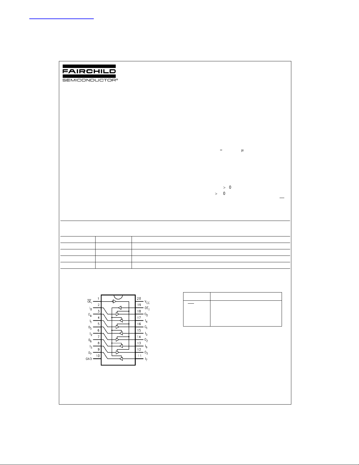
Connection Diagram Pin Descriptions
Pin Names Description
OE
O
, OE
1
I0–I
0–O7
7
3-STATE Output Enable Inputs
2
Inputs
Outputs
© 2005 Fairchild Semiconductor Corporation DS012639 www.fairchildsemi.com
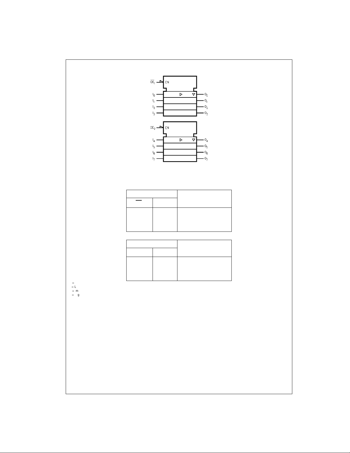
Logic Symbol
74LCX241
Truth Tables
H HIGH Voltage Level
LOW Volt age Level
L
Immaterial
X
High Impedance
Z
OE
1
Inputs
I
n
Outputs
(Pins 12, 14, 16, 18)
LL L
LH H
HX Z
OE
2
Inputs
I
n
Outputs
(Pins 3, 5, 7, 9)
HH H
HL L
LX Z
www.fairchildsemi.com 2
Absolute Maximum Ratings(Note 2)
Symbol Parameter Value Conditions Units
V
V
V
I
IK
I
OK
I
O
I
CC
I
GND
T
CC
I
O
STG
Supply Voltage
DC Input Voltage
DC Output Voltage
DC Input Diode Current
DC Output Diode Current
DC Output Source/Sink Current
DC Supply Current per Supply Pin
DC Ground Current per Ground Pin
Storage Temperature
0.5 to 7.0 V
0.5 to 7.0 V
0.5 to 7.0 Output in 3-STATE
0.5 to VCC 0.5 Output in HIGH or LOW State (Note 3)
50 V
50 V
50 V
r
50 mA
r
100 mA
r
100 mA
65 to 150
GND mA
I
GND
O
V
O
CC
mA
Recommended Operating Conditions (Note 4)
Symbol Parameter Min Max Units
V
CC
V
I
V
O
I
OH/IOL
T
A
't/'
Note 2: The Absolute Maximum Ratings are those values beyond which the safety of the device cannot be guaranteed. The device should not be operated
at these limits. The para metric va lues defined in the Elec trical Cha racteristic s tables are n ot guarantee d at the A bsolute Ma ximum R atings . The “Recom-
mended Operating Conditions” table will define the conditions for actual device operation.
Note 3: I
Note 4: Unused inputs must be he ld H I GH or LOW. They may not float.
Supply Voltage Operating 2.0 3 .6
Data Retention 1.5 3.6
V
Input Voltage 0 5.5 V
Output Voltage HIGH or LOW State 0 V
3-STATE 0 5.5
Output Current V
Free-Air Operating Temperature
3.0V 3.6V
CC
2.7V 3.0V
CC
2.3V 2.7V
V
CC
40 85
CC
r
24
r
12
r
8
V
mAV
q
C
V Input Edge Rate, VIN 0.8V2.0V, VCC 3.0V 0 10 ns/V
Absolute Maximum Rating must be observed.
O
V
q
C
74LCX241
DC Electrical Characteristics
Symbol Parameter Conditions
V
IH
V
IL
V
OH
V
OL
I
I
I
OZ
I
OFF
HIGH Level Input Voltage 2.3 2.7 1.7
LOW Level Input Voltage 2.3 2.7 0.7
HIGH Level Output Voltage IOH 100PA2.3
LOW Level Output Voltage IOL 100 PA2.3
Input Leakage Current 0 d VI d 5.5V 2.3 - 3.6
3-STATE Output Leakage 0 d VO d 5.5V
Power-Off Leakage Current VI or VO 5.5V 0 10
IOH 8 mA 2.3 1.8
IOH 12 mA 2.7 2.2
IOH 18 mA 3.0 2.4
IOH 24 mA 3.0 2.2
IOL 8 mA 2.3 0.6
IOL 12 mA 2.7 0.4
IOL 16 mA 3.0 0.4
IOL 24 mA 3.0 0.55
VI VIH or V
IL
V
CC
(V) Min Max
2.7 3.6 2.0
2.7 3.6 0.8
3.6 VCC - 0.2
3.6 0.2
2.3 - 3.6
TA 40qC to 85qC
Units
V
V
V
V
r
5.0
r
5.0
P
A
P
A
P
A
3 www.fairchildsemi.com
 Loading...