

Fairchild 74LCX16374 service manual
查询74LCX16374供应商
74LCX16374
Low Voltage 16-Bit D-Type Flip-Flop
with 5V Tolerant Inputs and Outputs
74LCX16374 Low Voltage 16-Bit D-Type Flip-Flop with 5V Tolerant Inputs and Outputs
February 1994
Revised May 2005
General Description
The LCX16374 contains sixteen non-inverting D-type
flip-flops with 3-STATE outputs and is intended for bus oriented applications. The dev ice is byte controlled. A buffered clock (CP) and Output E nable (OE
each byte and can be shorted together for full 16-bit operation.
The LCX16374 is designed for lo w voltage (2.5V or 3 .3V)
V
applications with capability of interfacing to a 5V signal
CC
environment.
The LCX16374 is fabricated with an advanced CMOS tech-
nology to achieve high speed operation whil e maintaining
CMOS low power dissipation.
) are common to
Features
■ 5V tolerant inputs and outputs
■ 2.3V–3.6V V
■ 6.2 ns t
■ Power down high impedance inputs and outputs
■ Supports live insertion/withdrawal (Note 1)
■
r
24 mA output drive (VCC 3.0V)
■ Uses patented noise/EMI reductio n circui tr y
■ Latch-up performance exce eds 500 mA
■ ESD performance:
Human body model ! 2000V
Machine model
■ Also packaged in plastic Fine-Pitch Ball Grid Array
(FBGA)
Note 1: To ensure the high-impedance state during power up or down, OE
should be tied to VCC through a pull-up res istor: the m inimu m value or t he
resistor is determined by the current-sourcing capability of the driver.
specifications provided
CC
max (VCC 3.3V), 20 PA ICC max
PD
!
200V
Ordering Code:
Order Number Package Number Package Description
74LCX16374G
(Note 2)(Note 3)
74LCX16374MEA
(Note 3)
74LCX16374MTD
(Note 3)
Note 2: Ordering code “G” indicates Trays.
Note 3: Devices also available in Tape and Reel. Specify by appending the suffix let te r “X” to the ordering code.
BGA54A 54-Ball Fine-Pitch Ball Grid Array (FBGA), JEDEC MO-205, 5.5mm Wide
MS48A 48-Lead Small Shrink Outline Package (SSOP), JEDEC MO-118, 0.300" Wide
MTD48 48-Lead Thin Shrink Small Outline Package (TSSOP), JEDEC MO-153, 6.1mm Wide
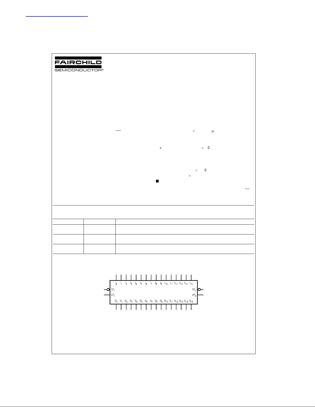
Logic Symbol
© 2005 Fairchild Semiconductor Corporation DS012003 www.fairchildsemi.com
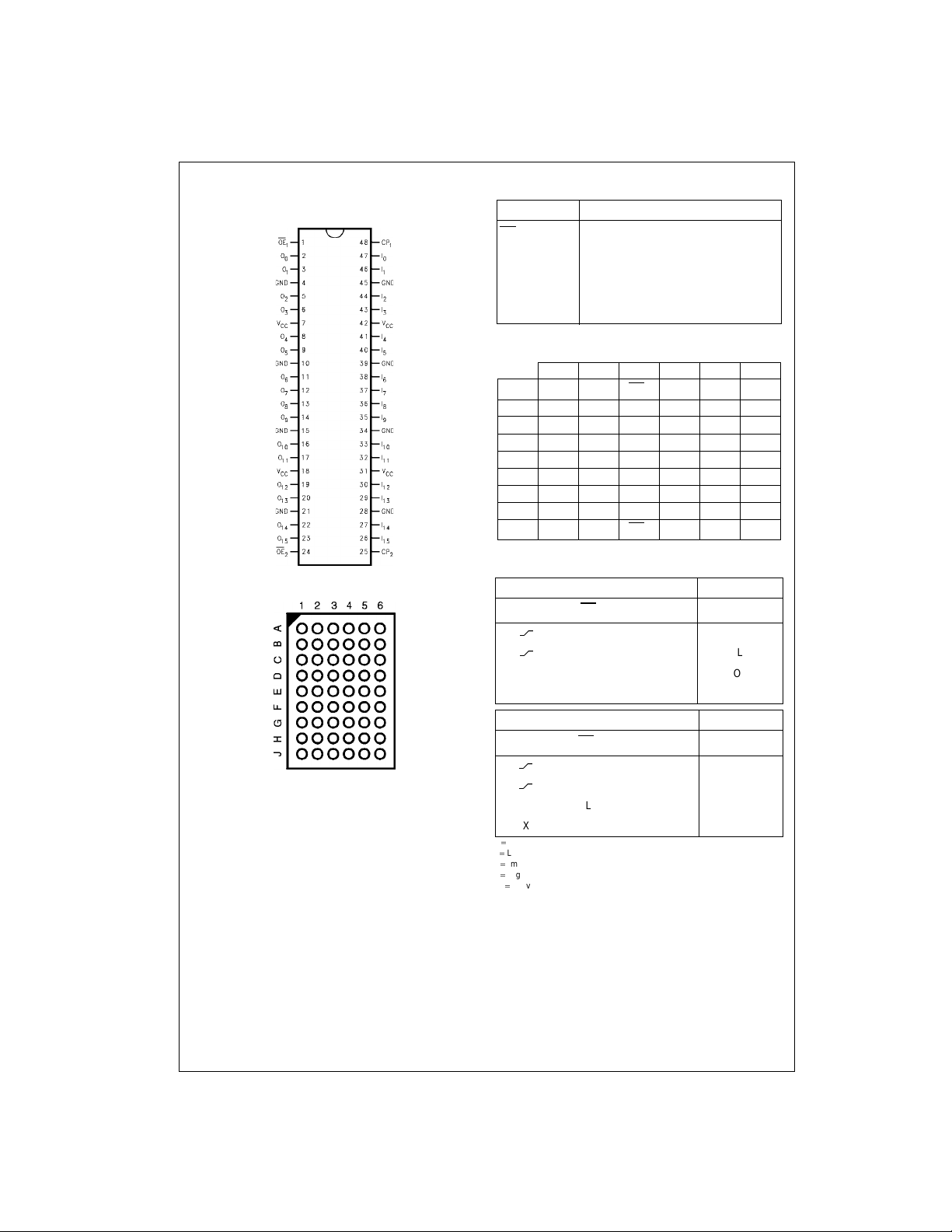
Connection Diagrams
Pin Descriptions
Pin Assignment for SSOP and TSSOP
74LCX16374
Pin Assignment for FBGA
Pin Names Description
OE
CP
I
0–I15
O
0–O15
n
n
Output Enable Input (Active LOW)
Clock Pulse Input
Inputs
Outputs
NC No Connect
FBGA Pin Assignments
123456
A O
B O
C O
D O
E O
F O
G O
H O
J O
NC OE1CP1NC I
0
O1NC NC I
2
O3V
4
6
8
10
12O11VCCVCCI11
14O13
15
CCVCCI3
O5GND GND I
O7GND GND I
O9GND GND I
NC NC I
NC OE2CP2NC I
1
5
7
9
13I14
Truth T ables
Inputs Outputs
CP
1
OE
1
LH H
LL L
LL X O
XH X Z
I0–I
7
O0–O
0
I
2
I
4
I
6
I
8
I
10
I
12
15
7
0
(Top Thru View)
www.fairchildsemi.com 2
Inputs Outputs
CP
2
OE
2
LH H
LL L
I8–I
15
O8–O
LL X O
XH X Z
H HIGH Voltage Level
LOW Voltage Level
L
X
Immaterial
High Impedance
Z
Previous O0 before HIGH-to-LOW of CP
O
0
15
0
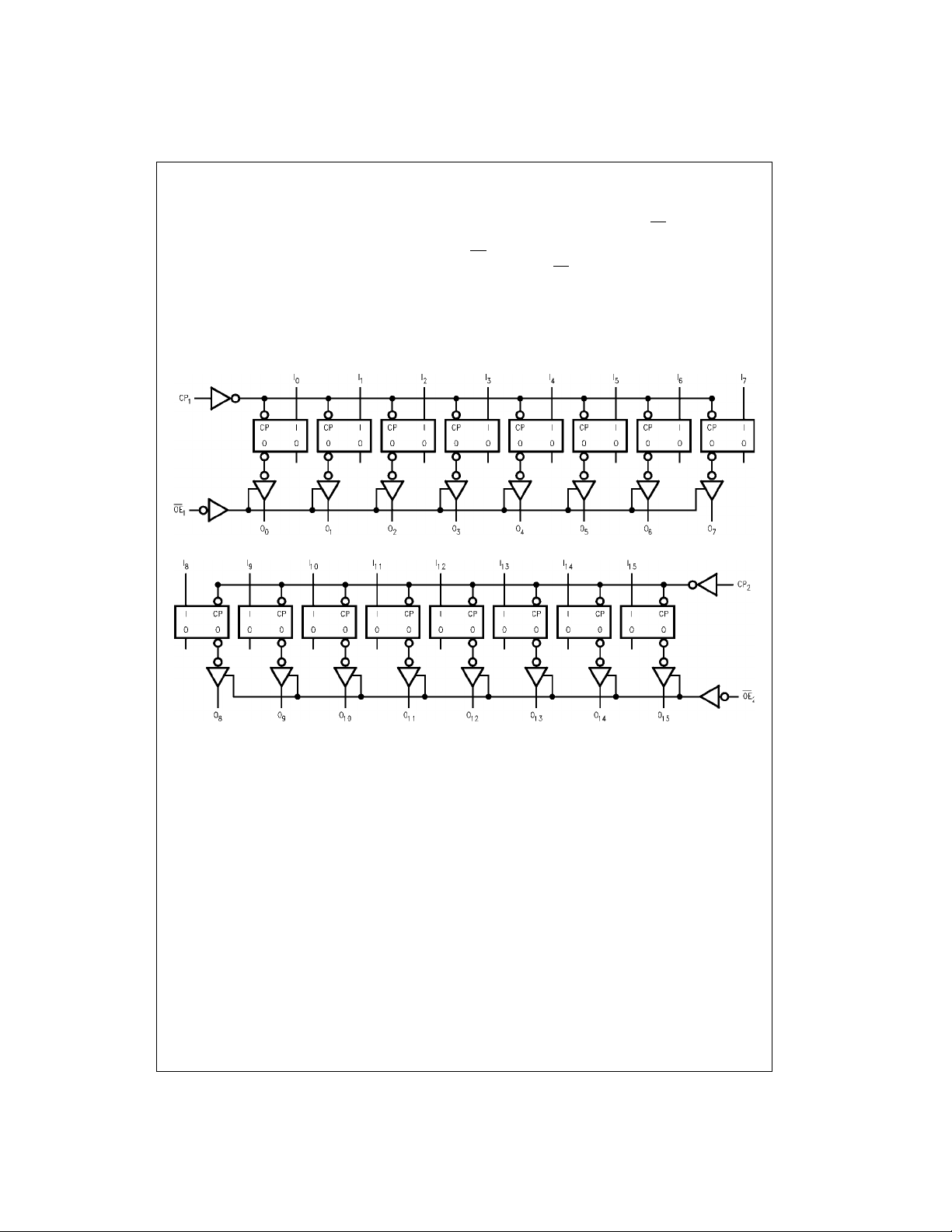
Functional Description
The LCX16374 con si sts of sixteen edge-triggered flip-flops
with individual D-type inputs and 3-STATE true outputs.
The device is byte controlled with each byte functioning
identically, but independent of the othe r. The control pins
can be shorted together to obtain full 16-bit operation. Each
byte has a buffered clock and buffered Output Enable common to all flip-flops within that by te. The description which
follows applies to each byte. Each flip-flop will store the
Logic Diagrams
Byte 1 (0:7)
Byte 2 (8:15)
state of their individu al D inputs that meet the set up and
hold time requirements on the LOW-to-HIGH Clock (CP
transition. With the Output Enable (OE
tents of the flip-flops are available at the outputs. When
OE
is HIGH, the outputs go to the high imped ance state.
n
Operation of the OE
flip-flops.
input does not affect t he state of the
n
) LOW, the con-
n
74LCX16374
)
n
Please note that this diagram is provided only for the understanding of logic operations and should not be used to estimate propagation delays .
3 www.fairchildsemi.com
 Loading...