Fairchild 74LCX162244 service manual

查询74LCX162244供应商
74LCX162244
Low Voltage 16-Bit Buffer/Line Driver
with 26
Ω Series Resistors in Outputs
74LCX162244 Low Voltage 16-Bit Buffer/Line Driver with 26
September 2000
Revised August 2001
General Description
The LCX162244 contains sixteen non-inverting buffers with
3-STATE outputs designed to be emplo yed as a memory
and address driver, clock driver, or bus oriented transmitter/receiver. The device is nibble contr olled. Each nibble
has separate 3-STATE control inputs which can be shorted
together for full 16-bit operation.
The LCX162244 is de si gn ed for l ow vo lt age ( 2.5 V or 3.3V)
V
applications with capability of interfacing to a 5V signal
CC
environment.
In addition, the outputs incl ude equivalent 26
series resistors to reduce overshoot and undershoot and
are designed to sink/source up to 12 mA at V
The LCX162244 is fabricated with an advanced CMOS
technology to achieve high speed operation while maintaining CMOS low power dissipation.
Ω (nominal)
= 3.0V.
CC
Features
■ 5V tolerant inputs and outputs
■ 2.3V–3.6V V
■ Outputs include equiv alent series resistance of 26
make external termination resistors unnecessary and
reduce overshoot and undershoot
■ 5.3 ns t
■ Power down high impedance inputs and outputs
±12 mA output drive (V
■
■ Implements patented noise/EMI reduction circuitry
■ Latch-up performance exce eds 500 mA
■ ESD performance:
Human body model > 2000V
Machine model
■ Also packaged in plastic Fine-Pitch Ball Grid Array
(FBGA) (Preliminary)
specifications provided
CC
max (VCC = 3.0V), 20 µA ICC max
PD
> 200V
Ordering Code:
Order Number Package Number Package Description
74LCX162244GX
(Note 1)
74LCX162244MEA
(Note 2)
74LCX162244MTD
(Note 2)
Note 1: BGA package available in Tape and Reel only.
Note 2: Devices also available in Tape and Reel. Specify by appending th e s uffix let t er “X” to the ordering code.
BGA54A
(Preliminary)
MS48A 48-Lead Small Shrink Outline Package (SSOP), JEDEC MO-118, 0.300" Wide
MTD48 48-Lead Thin Shrink Small Outline Package (TSSOP), JEDEC MO-153, 6.1mm Wide
54-Ball Fine-Pitch Ball Grid Array (FBGA), JEDEC MO-205, 5.5mm Wide
[TAPE and REEL]
= 3.0V)
CC
Ω to
Ω
Series Resistors in Outputs
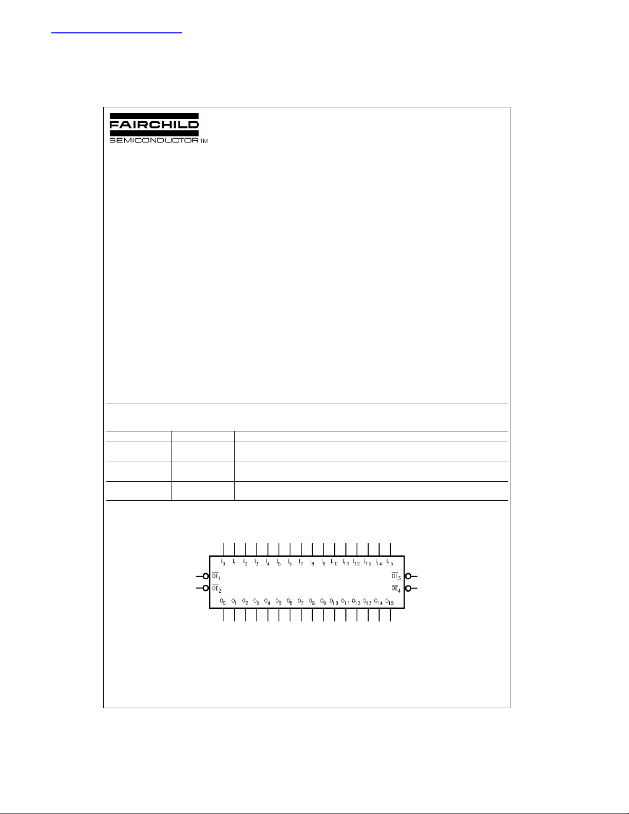
Logic Symbol
© 2001 Fairchild Semiconductor Corporation DS500471 www.fairchildsemi.com

Connection Diagrams
Pin Descriptions
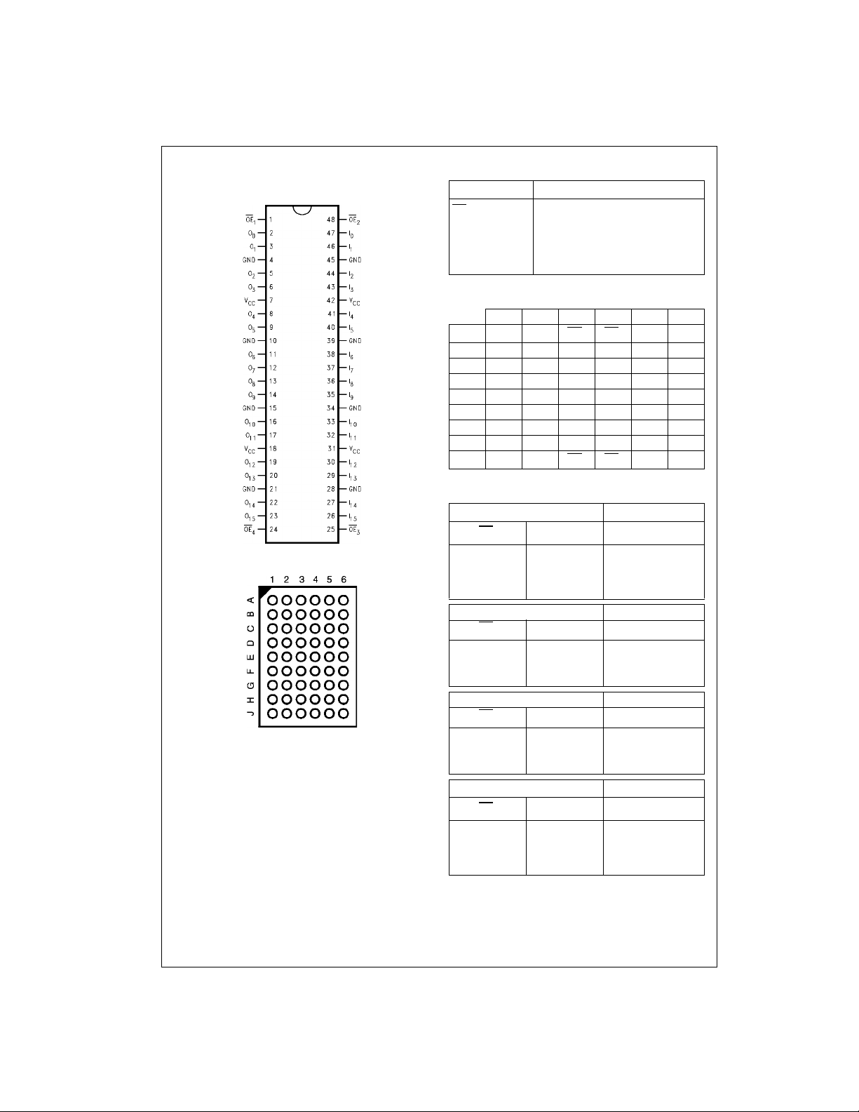
Pin Assignment for SSOP and TSSOP
74LCX162244
Pin Assignment for FBGA
(Top Thru View)
Pin Names Description
OE
I
0–I15
O
0–O15
n
Output Enable Input (Active LOW)
Inputs
Outputs
NC No Connect
FBGA Pin Assignments
123456
A O
B O
C O
D O
E O
F O
G O
H O
J O
NC OE1OE2NC I
0
O1NC NC I
2
O3V
4
6
8
10
12O11VCCVCCI11
14O13
15
CCVCCI3
O5GND GND I
O7GND GND I
O9GND GND I
NC NC I
NC OE4OE3NC I
Truth Tables
Inputs Outputs
OE
1
LL L
LH H
HX Z
Inputs Outputs
OE
2
LL L
LH H
HX Z
Inputs Outputs
OE
3
LL L
LH H
HX Z
Inputs Outputs
OE
4
LL L
LH H
HX Z
H = HIGH Voltage Level
L = LOW Voltage Level
X = Immaterial
Z = High Impedance
I0–I
I4–I
I8–I
I12–I
3
7
11
15
O8–O
O12–O
1
5
7
9
13I14
O0–O
3
O4–O
7
11
15
0
I
2
I
4
I
6
I
8
I
10
I
12
15
www.fairchildsemi.com 2

Functional Description
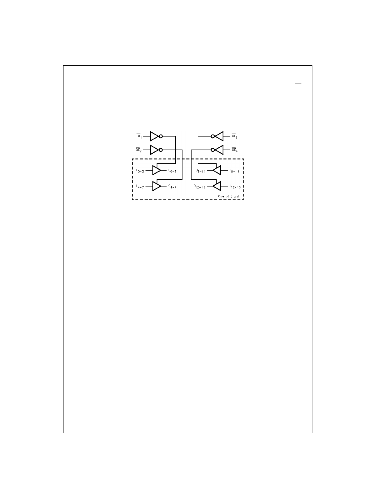
The LCX162244 contains sixteen non-inverting buffers with
3-STATE standard outputs. The device is designed with
26
Ω series resistors in the ou tputs. This design reduces
line noise in applications such as memor y addre ss drivers,
clock drivers and bus transceiver/transmitter s. The device
is nibble (4 bits) controlled with each nibble functioning
identically, but independent of the othe r. The control pins
Logic Diagram
can be shorted toge ther to obtain full 1 6-bit o peratio n. The
3-STATE outputs are controlled by an Output Enable (OE
input for each nibble. When OE
2-state mode. When OE
high impedance mode, but this does not interfere with
entering new data into the inputs.
is LOW, the outputs are in
n
is HIGH, the outputs are in the
n
74LCX162244
)
n
3 www.fairchildsemi.com
 Loading...