

Fairchild 74LCX06 service manual

查询74LCX06供应商
74LCX06
Low Voltage Hex Inve rte r/Buffer w ith Open Drain Outputs
74LCX06 Low Voltage Hex Inverter/Buffer with Open Drain Outputs
October 1999
Revised February 2005
General Description
The LCX06 contains six inverters/b uffers. The inputs tole rate voltages up to 7V allowing the interface of 5V syste ms
to 3V systems.
The outputs of the LCX06 are open drain an d can be connected to other open drain outputs to implement active
LOW wire AND or active HIGH wire OR functions.
The 74LCX06 is fabrica ted with advanced C MOS technology to achieve high speed operation while maintaining
CMOS low power dissipation.
Features
■ 5V tolerant inputs
■ 2.3V–3.6V V
■ 3.7 ns t
■ Power down high impedance inputs and outputs
■ 24 mA output drive (V
■ Implements patented noise/EMI reduction circuitry
■ Latch-up performance exce eds 500 mA
■ Functionally compatible with 74 series 05
■ ESD performance:
Human body model
Machine model ! 200V
specifications provided
CC
max (V
PD
CC
3.3V), 10 PA ICC max
3.0V)
CC
!
2000V
Ordering Code:
Order Number
74LCX06M M14A 14-Lead Small Outline Integrated Circuit (SOIC), JEDEC MS-012, 0.150" Narrow
74LCX06MX_NL
(Note 1)
74LCX06SJ M14D Pb-Fr ee 14 -Lead Small Outline Package (SOP), EIAJ TYPE II, 5.3mm Wide
74LCX06MTC MTC14 14-Lead Thin Shrink Small Outline Package (TSSOP), JEDEC MO-153, 4.4mm Wide
74LCX06MTCX_NL
(Note 1)
Devices also availab l e in Tape and Reel. Specify by appending the suffix let t er “X” to the ordering code.
Pb-Free package per JEDEC J-STD-020B.
Note 1: “_NL” indicates Pb-Free pac k age (per JEDEC J-S T D -020B). Device available in Tape and Reel only.
Package
Number
M14A Pb-Free 14-Lead Small Outline Integrated Circuit (SOIC), JEDEC MS-012, 0.150" Narrow
MTC14 Pb-Free 14-Lead Thin Shrink Small Outline Package (TSSOP), JEDEC MO-153, 4.4mm Wide
Package Description
Logic Symbol
IEEE/IEC
Connection Diagram
Pin Descriptions
Pin Names Description
A
n
O
n
© 2005 Fairchild Semiconductor Corporation DS500237 www.fairchildsemi.com
Inputs
Outputs
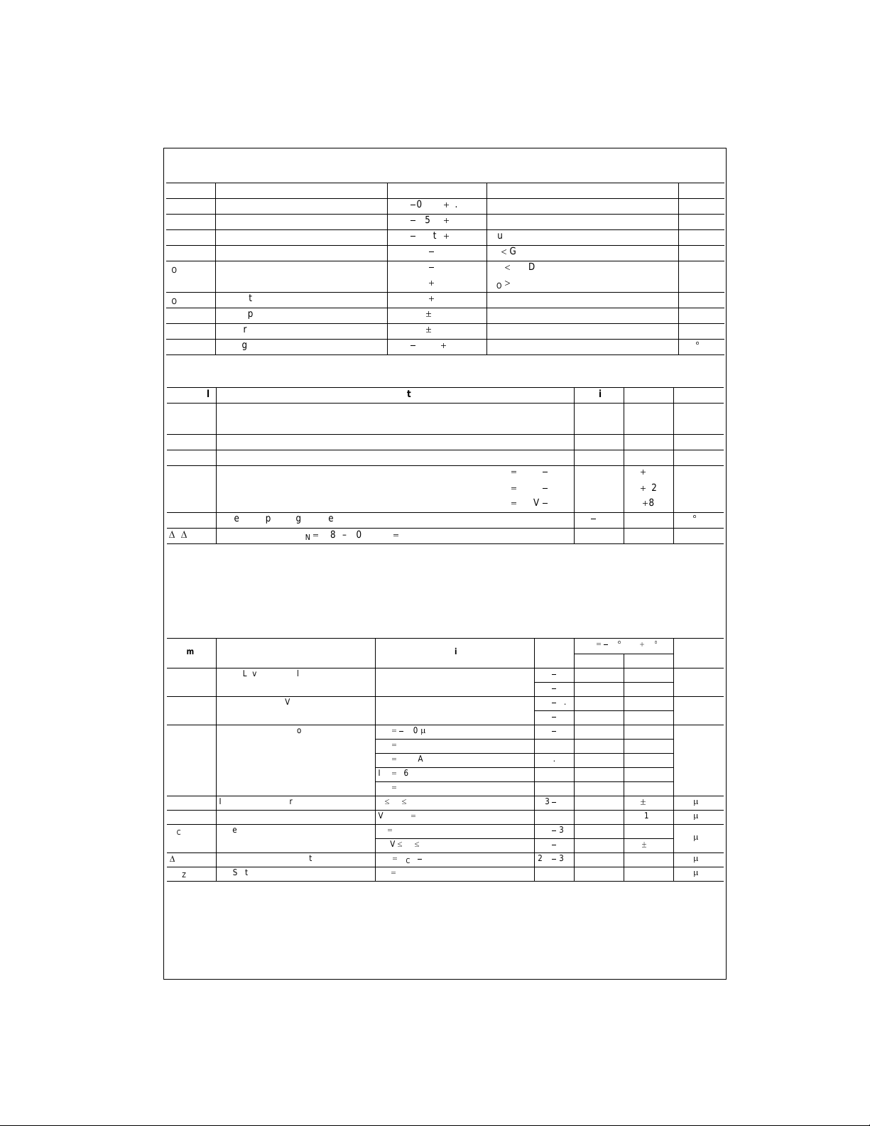
Absolute Maximum Ratings(Note 2)
Symbol Parameter Value Conditions Units
74LCX06
V
V
V
I
I
I
I
I
T
CC
I
O
IK
OK
O
CC
GND
STG
Supply Voltage
DC Input Voltage
DC Output Voltage
DC Input Diode Current
DC Output Diode Current
DC Output Sink Current
DC Supply Current per Supply Pin
DC Ground Cu rrent per Ground Pin
Storage Temperature
0.5 to 7.0 V
0.5 to 7.0 V
0.5 to 7.0 Output in HIGH or LOW State (Note 3) V
50 VI GND mA
50 VO GND
50 VO ! V
50 mA
r
100 mA
r
100 mA
65 to 150
CC
Recommended Operating Conditions (Note 4)
Symbol Parameter Min Max Units
V
CC
V
I
V
O
I
OL
T
A
't/'
Note 2: The Absolute Maximum Ratings are those values beyond which the safety of the device cannot be guaranteed. The device should not be operated
at these limits. The parametric va lues defin ed in the El ectrical C haracteris tics tables are not guara nteed at the Absolute M aximum Ratings. The “Recom-
mended Operat ing Conditions” table will define the conditions fo r ac t ual device operation.
Note 3: I
Note 4: Unused inputs must be held HIGH or LOW. They may not fl oat .
Supply Voltage Operating 2.0 3.6
Data Retention 1.5 3.6
Input Voltage 05.5V
Output Voltage 0 5.5 V
Output Current VCC 3.0V 3.6V
2.7V 3.0V
CC
2.3V 2.7V
V
CC
Free-Air Operating Temperature
40 85
24
12
8
V Input Edge Rate, VIN 0.8V–2.0V, VCC 3.0V 0 10 ns/V
Absolute Maximum Rating must be observed.
O
mAV
mA
q
q
C
V
C
DC Electrical Characteristics
Symbol Parameter Conditions
V
IH
V
IL
V
OL
I
I
I
OFF
I
CC
'
I
I
OHZ
www.fairchildsemi.com 2
HIGH Level Input Voltage 2.3 2.7 1.7
LOW Level Input Voltage 2.3 2.7 0.7
LOW Level Output Voltage IOL 100 PA2.3
IOL 8 mA 2.3 0.6
IOL 12 mA 2.7 0.4
IOL 16 mA 3.0 0.4
Input Leakage Current 0 d VI d 5.5V 2.3 3.6
Power-Off Leakage Current VI or VO 5.5V 0 10
Quiescent Supply Current VI VCC or GND 2.3 3.6 10
Increase in ICC per Input VIH VCC 0.6V 2.3 3.6 500
CC
Off State Current VO 5.5 2 - 3.6 10
IOL 24 mA 3.0 0.55
3.6V d VI d 5.5V 2.3 3.6
V
(V) Min Max
2.7 3.6 2.0
2.7 3.6 0.8
40qC to 85qC
CCTA
3.6 0.2
r
r
5.0
Units
V
V
V
P
A
P
A
P
10
A
P
A
P
A

AC Electrical Characteristics
Symbol Parameter
t
PZL
t
PLZ
Propagation Delay Time 0.8 3.7 1.0 4.1 0.8 3.5
40qC to 85qC, RL 500
T
V
3.3V r 0.3V VCC 2.7V VCC 2.5V r 0.2V
CC
50 pF CL 50 pF CL
C
L
Min Max Min Max Min Max
0.8 3.7 1.0 4.1 0.8 3.5
A
:
30 pF
Dynamic Switching Characteristics
Symbol Parameter Conditions
V
OLP
V
OLV
Quiet Output Dynamic Peak V
Quiet Output Dynamic Valley V
OL
OL
CL 50 pF, VIH 3.3V, VIL 0V 3.3 0.9
C
30 pF, VIH 2.5V, VIL 0V 2.5 0.7
L
CL 50 pF, VIH 3.3V, VIL 0V 3.3
CL 30 pF, VIH 2.5V, VIL 0V 2.5
V
(V) Typical
CCTA
25qC
0.8
0.6
Capacitance
Symbol Parameter Conditions Typical Units
C
IN
C
OUT
C
PD
Input Capacitance VCC Open, VI 0V or V
Output Capacitance VCC 3.3V, VI 0V or V
Power Dissipation Capacitance VCC 3.3V, VI 0V or VCC, f 10 MHz 25 pF
CC
CC
7pF
8pF
74LCX06
Units
ns
Units
V
V
3 www.fairchildsemi.com
 Loading...