

Fairchild 74F160A service manual
查询74F160A供应商
74F160A • 74F162A
Synchronous Presettable BCD Decade Counter
74F160A • 74F162A Synchronous Presettable BCD Decade Counter
April 1988
Revised July 1999
General Description
The 74F160A and 74F 162A are high-speed synchr onous
decade counters operat ing in the BCD (8421) sequence.
They are synchronously p rese tta ble fo r ap pl ica ti on s in pr ogrammable dividers. Ther e are two types of Count E nable
inputs plus a T erminal Count output for versatility in forming
synchronous multistage counters. The F160A has an asynchronous Master Rese t inp ut t hat overrides all other inp uts
and forces the outputs LOW. The F162A ha s a Synchronous Reset input that overrides cou nting an d paral lel loading and allows all outputs to be simultaneously reset on the
rising edge of th e clock. The F160A and F162A are high
speed versions of the F160 and F162.
Features
■ Synchronous counting and loading
■ High-speed synchronous expan si on
■ Typical count rate of 120 MHz
Ordering Code:
Order Number Package Number Package Description
74F160ASC M16A 16-Lead Small Outline Integrated Circuit (SOIC), JEDEC MS-012, 0.150 Narrow
74F160ASJ M16D 16-Lead Small Outline Package (SOP), EIAJ TYPE II, 5.3mm Wide
74F160APC N16E 16-Lead Plastic Dual-In-Line Package (PDIP), JEDEC MS-001, 0.300 Wide
74F162ASC M16A 16-Lead Small Outline Integrated Circuit (SOIC), JEDEC MS-012, 0.150 Narrow
74F162APC N16E 16-Lead Plastic Dual-In-Line Package (PDIP), JEDEC MS-001, 0.300 Wide
Devices also availab le in Tape and Reel. Specify by appending th e s uffix let t er “X” to the ordering cod e.
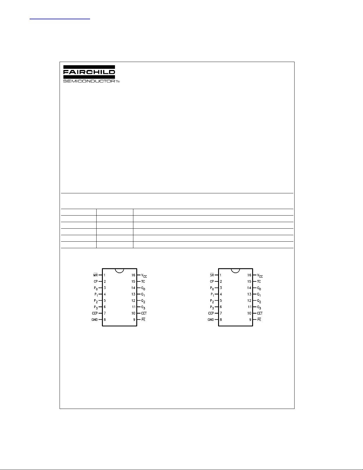
Connection Diagrams
74F160A 74F162A
© 1999 Fairchild Semiconductor Corporation DS009485 www.fairchildsemi.com
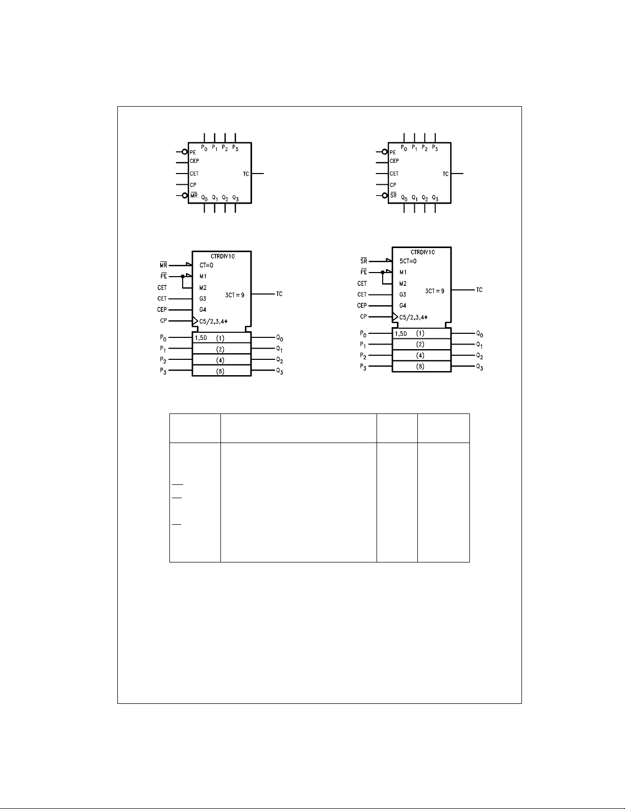
Logic Symbols
74F160A • 74F162A
74F160A
IEEE/IEC
74F162A
74F160A
Unit Loading/Fan Out
Pin Names Description
CEP Count Enable Parallel Input 1.0/1.0 20 µA/−0.6 mA
CET Count Enable Trickle Input 1.0/2.0 20 µA/−1.2 mA
CP Clock Pulse Input (Active Rising Edge) 1.0/1.0 20 µA/−0.6 mA
(74F160A) Asynchronous Master Reset Input (Active LOW) 1.0/1.0 20 µA/−0.6 mA
MR
(74F162A) Synchronous Reset Input (Active LOW) 1.0/2.0 20 µA/−1.2 mA
SR
P
0–P3
PE
Q
0–Q3
TC Terminal Count Output 50/33.3 −1 mA/20 mA
Parallel Data Inputs 1.0/1.0 20 µA/−0.6 mA
Parallel Enable Input (Active LOW) 1.0/2.0 20 µA/−1.2 mA
Flip-Flop Outputs 50/33.3 −1 mA/20 mA
74F162A
U.L.
HIGH/LOW
Input I
Output I
IH/IIL
OH/IOL
www.fairchildsemi.com 2
Functional Description
The 74F160A and 74F162A count modulo-10 in the BCD
(8421) sequence. From st ate 9 (HLLH) they increment to
state 0 (LLLL). The clock inputs of all flip-flops are driven in
parallel through a cl ock buffer. Thus all changes of the Q
outputs (except due to Master Reset of the (F160A) occ ur
as a result of, and synchronous with, the LOW-to-HIGH
transition of the CP input signal. The circuits have four fundamental modes of operation, in order of precedence:
asynchronous reset ( F160A), synchronous reset (F162A),
parallel load, count-up and hold . Five con trol in puts—Ma ster Reset (MR
Parallel Enable (PE
Count Enable Trickle (CET )—det ermi ne the mode of ope ration, as shown in the Mode Select Table. A LOW signal on
overrides all other inputs and asynchronously forces all
MR
outputs LOW. A LOW signal on SR
parallel loading and allows all outputs to go LOW o n the
next rising edge of CP. A LOW signal on PE
counting and allows information on the Parallel Data (P
inputs to be loaded into the flip-flops on the next rising
edge of CP. With PE
HIGH, CEP and CET pe rmit counting when both are HIG H.
Conversely, a LOW signal on either CE P or CET inhibits
counting.
, F160A), Synchrono us Reset (SR, F162A),
), Count Enable Parallel (CEP) and
overrides counting and
overrides
and MR (F160A) or SR (F162A)
The F160A and F162A use D-type edge-triggered flip-flops
and changing the S R
CP is in either state does not cause error s, provided that
the recommended setup and hold times, with respect to the
rising edge of CP, are observed.
The Terminal Count (TC) output is HIGH when CET is
HIGH and counter is in state 9. To implement synchronous
multistage counters, the TC outputs can be used w ith the
CEP and CET inputs in two different ways. Please ref er to
the F568 data sheet. The TC o utput is su bje ct to deco ding
spikes due to internal race conditions and is there fore not
recommended for use as a clock or asynchronous reset for
flip-flops, counters or re gisters. In the F160A and F162A
decade counters, the TC output is fully decoded and can
only be HIGH in state 9. If a decade counter is preset to an
illegal state, or assumes an illegal state when power is
applied, it will return to the normal sequence within two
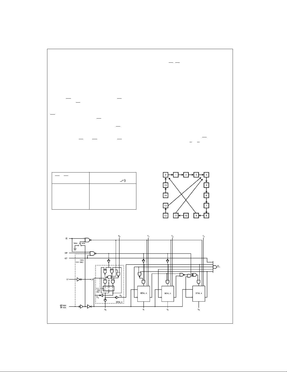
counts, as shown in the State Diagr am.
)
n
Logic Equations:
Count Enable = CEP × CET × PE
, PE, CEP and CET inputs when the
TC = Q0 × Q 1× Q 2 × Q3 × CET
74F160A • 74F162A
Mode Select Table
*SR PE CET CEP
L X X X Reset (Clear)
H L X X Load (P
H H H H Count (Increment)
H H L X No Change (Hold)
H H X L No Change (Hold)
*For 74’F162A only
H = HIGH Voltage Level
L = LOW Voltage Level
X = Immaterial
Action on the Rising
Clock Edge (
n
Logic Diagram
→ Qn)
State Diagram
)
Please note that this d iagram is provided only f or t he understanding of lo gic operations and shou ld not be used to estimate propagation delays.
3 www.fairchildsemi.com
 Loading...