

查询74F151供应商
74F151A
8-Input Multiplexer
74F151A 8-Input Multiplexer
April 1988
Revised March 1999
General Description
The F151A is a high-speed 8-input digital multiplexer. It
provides in one p ackage the ability to select one line of
data from up to eight sources. The F151A can be used as a
universal function g enerator to generate any logic function
of four variables. Both a ssertion and negation outputs are
provided.
Ordering Code:
Order Number Package Number Package Description
74F151ASC M16A 16-Lead Small Outline Integrated Circuit (SOIC), JEDEC MS-012, 0.150 Narrow
74F151ASJ M16D 16-Lead Small Outline Package (SOP), EIAJ TYPE II, 5.3mm Wide
74F151APC N16E 16-Lead Plastic Dual-In-Line Package (PDIP), JEDEC MS-001, 0.300 Wide
Devices also availab le in Tape and Reel. Specify by appending th e s uffix let t er “X” to the ordering code.
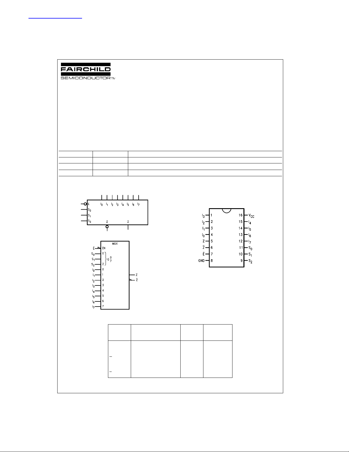
Logic Symbols
Connection Diagram
IEEE/IEC
Unit Loading/Fan Out
Pin Names Description
I0–I
S
0–S2
E
Z Data Output 50/33.3 −1 mA/20 mA
Z
© 1999 Fairchild Semiconductor Corporation DS009481.prf www.fairchildsemi.com
Data Inputs 1.0/1.0 20 µA/−0.6 mA
7
Select Inputs 1.0/1.0 20 µA/−0.6 mA
Enable Input (Active LOW) 1.0/1.0 20 µA/−0.6 mA
Inverted Data Output 50/33.3 −1 mA/20 mA
U.L. Input I
HIGH/LOW Output IOH/I
IH/IIL
OL
Functional Description
The F151A is a logic implementation of a single pole, 8position switch with the switch position controlled by the
state of three Selec t inputs, S
74F151A
, S1, S2. Both assertion and
0
negation outputs are provided. The Enable input (E
active LOW. When it is not activated, the negation output is
HIGH and the assertio n output is LOW regardless of all
other inputs. The logic function provided at the output is:
• (I0S2S1S0+ I1S2S1S0+ I2S2S1S0+
Z = E
I
3S2S1S0
I
6S2S1S0
+ I4S2S1S0+ I5S2S1S0+
+ I7S2S1S0)
The F151A pro vides the ability, in one packag e, to select
from eight sources of data or control information. By proper
manipulation of the inputs, the F151A can provide any logic
function of four variables and its negation.
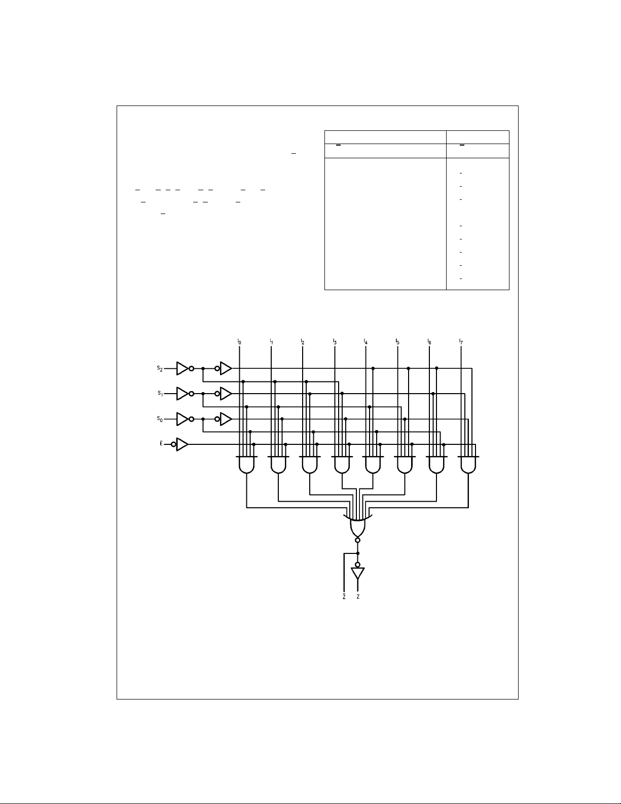
Logic Diagram
Truth Table
) is
H = HIGH Voltage Level
L = LOW Voltage Level
X = Immaterial
Inputs Outputs
S
E
S
2
S
1
Z Z
0
HXXXHL
LLLLI
LL LHI1I
LLH LI2I
LLHHI3I
LH L L I4I
LH L H I5I
LHH L I6I
LHH H I7I
I
0
0
1
2
3
4
5
6
7
Please note that this diagram is provided o nly f or t he understanding of logic operations and shou ld not be used to estimate propagation delays.
www.fairchildsemi.com 2
 Loading...