

Fairchild 74F139 service manual
查询74F139PC供应商
74F139
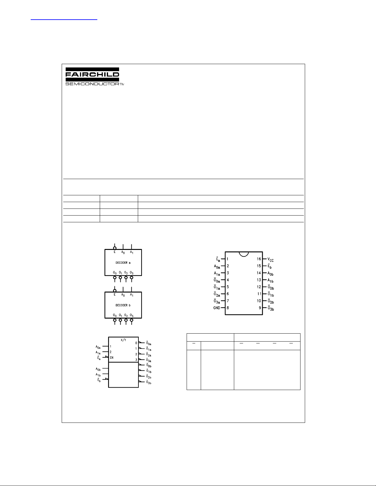
Dual 1-of-4 Decoder/Demultiplexer
74F139 Dual 1-of-4 Decoder/Demultiplexer
April 1988
Revised July 1999
General Description
The F139 is a high-speed, dual 1-of-4 decoder/demultiplexer. The device has two indepen dent decoders, each
accepting two inputs and provi ding four m utually exclu sive
active LOW outputs. Each decoder has an active LOW
Enable input which can be used as a data input for a 4-output demultiplexer. Each half of the F1 39 can be u sed as a
function generator pr oviding all four minte rms of two variables.
Features
■ Multifunction capability
■ Two completely independent 1-of-4 decoders
■ Active LOW mutually exclusive outputs
Ordering Code:
Order Number Package Number Package Description
74F139SC M16A 16-Lead Small Outline Integrated Circuit (SOIC), JEDEC MS-012, 0.150 Narrow
74F139SJ M16D 16-Lead Small Outline Package (SOP), EIAJ TYPE II, 5.3mm Wide
74F139PC N16E 16-Lead Plastic Dual-In-Line Package (PDIP), JEDEC MS-001, 0.300 Wide
Devices also availab le in Tape and Reel. Specify by appending th e s uffix let t er “X” to the ordering cod e.
Logic Symbols
Connection Diagram
IEEE/IEC
© 1999 Fairchild Semiconductor Corporation DS009479 www.fairchildsemi.com
Inputs Outputs
A
A
O
O
O
E
0
1
0
1
HXXHHHH
LLLLHHH
LHLHLHH
LLHHHLH
LHHHHHL
H = HIGH Voltage Level
L = LOW Voltage Level
X = Immaterial
O
2
3
Truth Table
Unit Loading/Fan Out
74F139
Pin Names Description
A0, A
E
O
0–O3
Address Inputs 1.0/1.0 20 µA/−0.6 mA
1
Enable Inputs (Active LOW) 1.0/1.0 20 µA/−0.6 mA
Outputs (Active LOW) 50/33.3 −1 mA/20 mA
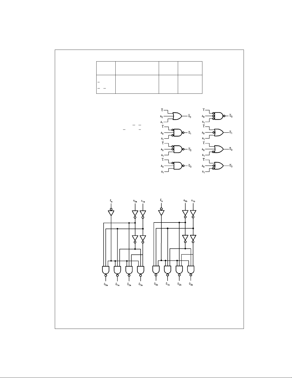
Functional Description
The F139 is a high-speed dual 1-of-4 decoder/demultiplexer. The device has two independent deco ders, eac h of
which accepts two binary weighted inputs (A
vides four mutually exclusive active LOW Outputs (O
Each decoder has an active LOW enable (E
HIGH all outp ut s are f or c ed HIG H . Th e en a bl e can be u s ed
as the data input for a 4-outp ut demultiplexer applicatio n.
Each half of the F139 generates all four minterms of two
variables. These four minte rm s are use ful in so me a ppl ica tions, replacing multiple gate functions as shown in
Figure 1, and thereby reducing the number of packages
required in a logic network.
0–A1
). When E is
Logic Diagram
) and pro-
0–O3
U.L.
HIGH/LOW
).
FIGURE 1. Gate Functions (each half)
Input I
Output I
IH/IIL
OH/IOL
Please note that this diagram is provided o nly f or t he understanding of lo gic operations and shou ld not be used to estimate propagation delays.
www.fairchildsemi.com 2
 Loading...