Fairchild 74F114 service manual

查询74F114供应商
74F114
Dual JK Negative Edge-Triggered Flip-Flop
with Common Clocks and Clears
74F114 Dual JK Negative Edge-Triggered Flip-Flop
April 1988
Revised August 1999
General Description
The 74F114 contains two high-speed JK flip-flops with
common Clock and Clear inputs. Synchronous state
changes are initiated by the falling edge of the clock. Triggering occurs at a voltage level of the clock and is not
directly related to th e transition time. The J and K i nputs
can change when the clock is in either state wi thout affecting the flip-flop, provided tha t they are in the desired sta te
during the recommen ded setup and hold time s relative to
the falling edge of the clock. A LOW signal on S
prevents clocking and forces Q or Q HIGH, respectively.
or C
D
Simultane o us LO W signals on S
HIGH.
Q
Asynchronous Inputs:
LOW input to S
LOW input to C
Clear and Set are independent of Clock
Simultaneous LOW on C
D
makes both Q and Q HIGH
sets Q to HIGH level
D
sets Q to LOW level
D
and CD force both Q and
D
and S
D
D
Ordering Code:
Order Number Package Number Package Description
74F114SC M14A 14-Lead Small Outline Integrated Circuit (SOIC), JEDEC MS-120, 0.150 Narrow
74F114PC N14A 14-Lead Plastic Dual-In-Line Package (PDIP), JEDEC MS-001, 0.300 Wide
Devices also availab le in Tape and Reel. Specify by appending th e s uffix let t er “X” to the ordering cod e.
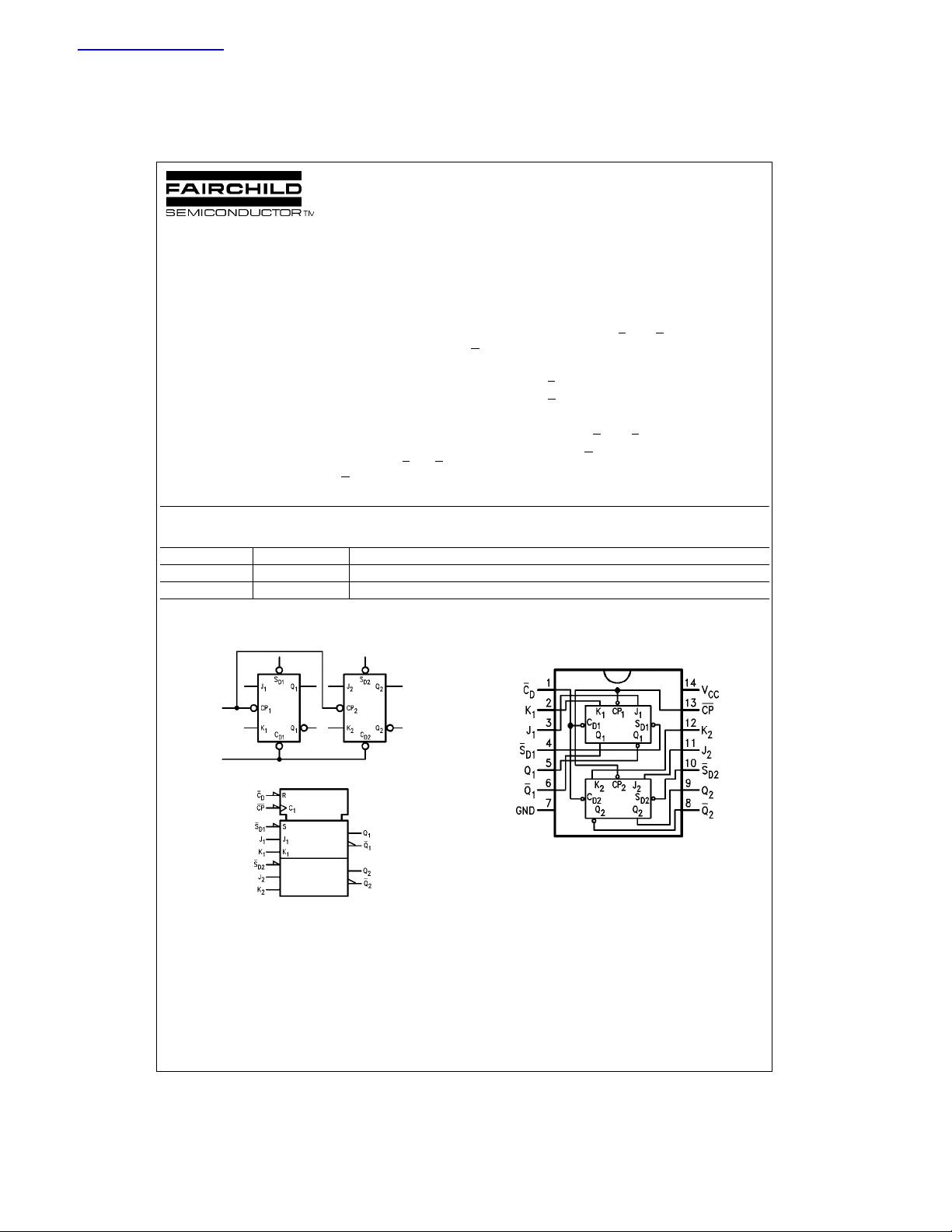
Logic Symbols
IEEE/IEC
Connection Diagram
© 1999 Fairchild Semiconductor Corporation DS009474 www.fairchildsemi.com

Unit Loading/Fan Out
74F114
Pin Names Description
U.L. Input I
HIGH/LOW Output IOH/I
J1, J2, K1, K2Data Inputs 1.0/1.0 20 µA/−0.6 mA
CP
C
D
, S
S
D1
D2
, Q2, Q1, Q2Outputs 50/33.3 −1 mA/20 mA
Q
1
Clock Pulse Input (Active Falling Edge) 1.0/8.0 20 µA/−4.8 mA
Direct Clear Input (Active LOW) 1.0/10.0 20 µA/−6.0 mA
Direct Set Inputs (Active LOW) 1.0/5.0 20 µA/−3.0 mA
Truth Table
Inputs Outputs
CDCP JKQQ
S
D
LHXXXHL
HLXXXLH
LLXXXHH
HH
HH
HH
HH
H (h) = HIGH Voltage Level
L (h) = LOW Voltage Level
X = Immaterial
= HIGH-to-LOW C loc k Transit ion
Q
(Q0) = Before HIGH-to-LOW Transition of Clock
0
Lower case letters indicate the state of the ref erenced input or outp ut one setup time prior to the HI GH-to-LOW clock tra ns it io n.
hhQ0Q
lhLH
hlHL
llQ0Q
0
0
IH/IIL
OL
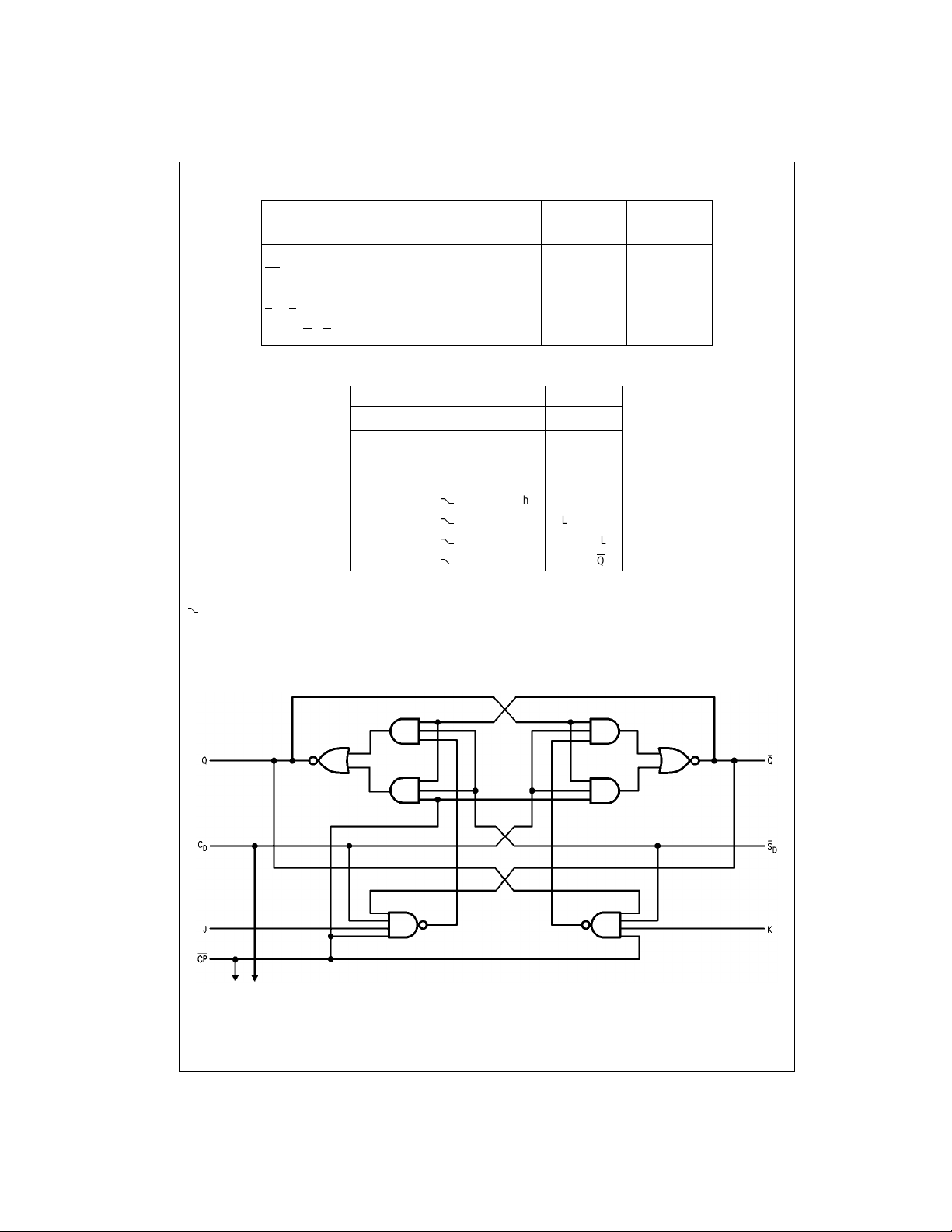
Logic Diagram
(one half shown)
Please note that this diagram is provided o nly f or t he understanding of lo gic operations and shou ld not be used to estimate propagation delays.
www.fairchildsemi.com 2
 Loading...