

Fairchild 74F11 service manual
查询74F11供应商
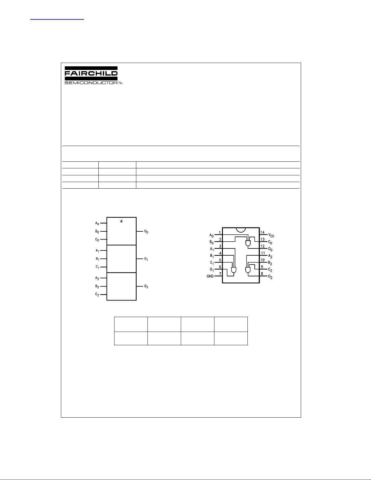
74F11
Triple 3-Input AND Gate
General Description
This device contains three independent gates, each of
which performs the logic AND function.
Ordering Code:
Order Number Package Number Package Description
74F11SC M14A 14-Lead Small Outline Integrated Circuit (SOIC), JEDEC MS-120, 0.150 Narrow
74F11SJ M14D 14-Lead Small Outline Package (SOP), EIAJ TYPE II, 5.3mm Wide
74F11PC N14A 14-Lead Plastic Dual-In-Line Package (PDIP), JEDEC MS-001, 0.300 Wide
Devices also available in Tape and Reel . Specify by appending the suffix letter “X” to the ordering code.
74F11 Triple 3-Input AND Gate
April 1988
Revised July 1999
Logic Symbol
IEEE/IEC
Unit Loading/Fan Out
Pin Names Description
An, Bn, C
O
n
Connection Diagram
U.L.
HIGH/LOW
Inputs 1.0/1.0 20 µA/−0.6 mA
n
Outputs 50/33.3 −1 mA/20 mA
Input I
Output I
IH/IIL
OH/IOL
© 1999 Fairchild Semiconductor Corporation DS009459 www.fairchildsemi.com
Absolute Maximum Ratings(Note 1) Recommended Operating
74F11
Storage Temperature −65°C to +150°C
Ambient Temperature under Bias −55°C to +125°C
Junction Temperature under Bias −55°C to +150°C
V
Pin Potential to Ground Pin −0.5V to +7.0V
CC
Input Voltage (Note 2) −0.5V to +7.0V
Input Current (Note 2) −30 mA to +5.0 mA
Voltage Applied to Output
in HIGH State (with V
CC
= 0V)
Standard Output −0.5V to V
3-STATE Output −0.5V to +5.5V
Current Applied to Output
in LOW State (Max) twice the rated I
OL
Conditions
Free Air Ambient Temperature 0°C to +70°C
Supply Voltage +4.5V to +5.5V
Note 1: Absolute maximum ratings are values beyond which the device
may be damaged or have its useful life impaired. Functional operation
CC
under these conditions is not implied.
Note 2: Either v oltage limit or current limit is sufficient to protect inputs.
(mA)
DC Electrical Characteristics
Symbol Parameter Min Typ Max Units
V
V
V
V
V
I
I
I
V
I
I
I
I
I
IH
IL
CD
OH
OL
IH
BVI
CEX
ID
OD
IL
OS
CCH
CCL
Input HIGH Voltage 2.0 V Recognized as a HIGH Signal
Input LOW Voltage 0.8 V Recognized as a LOW Signal
Input Clamp Diode Voltage −1.2 V Min IIN = −18 mA
Output HIGH 10% V
Voltage 5% V
Output LOW 10% V
Voltage
Input HIGH
Current
Input HIGH Current
Breakdown Test
Output HIGH
Leakage Current
Input Leakage
Test All other pins grounded
Output Leakage
Circuit Current All other pins grounded
Input LOW Current −0.6 mA Max VIN = 0.5V
Output Short-Circuit Current −60 −150 mA Max V
Power Supply Current 4.1 6.2 mA Max VO = HIGH
Power Supply Current 6.5 9.7 mA Max VO = LOW
CC
CC
CC
2.5 V Min IOH = −1 mA
2.7 IOH = −1 mA
0.5 V Min IOL = 20 mA
5.0 µAMaxVIN = 2.7V
7.0 µAMaxVIN = 7.0V
50 µAMaxV
4.75 V 0.0
3.75 µA0.0
AC Electrical Characteristics
Symbol Parameter
t
PLH
t
PHL
Propagation Delay 3.0 4.2 5.6 2.5 7.5 3.0 6.6
An, Bn, Cn to O
TA = +25°CT
VCC = +5.0V VCC = +5.0V VCC = +5.0V
CL = 50 pF CL = 50 pF CL = 50 pF
Min Typ Max Min Max Min Max
n
2.5 4.1 5.5 2 .0 7.5 2.5 6.5
−55°C to +125°CTA = 0°C to +70°C
A
V
CC
= V
OUT
IID = 1.9 µA
V
= 150 mV
IOD
= 0V
OUT
Conditions
CC
Units
ns
www.fairchildsemi.com 2
 Loading...