Fairchild 74ACQ374 service manual

查询74ACQ374供应商查询74ACQ374供应商
74ACQ374 • 74ACTQ374
Quiet Series Octal D-Type Flip-Flop
with 3-STATE Outputs
74ACQ374 • 74ACTQ374 Quiet Series Octal D-Type Flip-Flop with 3-STATE Outputs
July 1989
Revised November 1999
General Description
The ACQ/ACTQ37 4 is a high-speed, low-po wer octal Dtype flip-flop featuring separate D-t ype inputs for each flipflop and 3-STATE outputs for bus-oriented app lications. A
buffered Clock (CP) and Output Enable (OE
to all flip-flops.
The ACQ/ACTQ374 utilizes FACT Quiet Series technology to guarantee quiet output switching and improve
dynamic threshold performance. FACT Quiet Series features GTO output control and undershoot corrector in
addition to a split ground bus for superior performance.
) are common
Features
■ ICC and IOZ reduced by 50%
■ Guaranteed simultaneous switching noise level and
dynamic threshold performan ce
■ Guaranteed pin-to-pin skew AC performance
■ Improved latch-up immunity
■ Buffered positive edge-triggered cl ock
■ 3-STATE outputs drive bus lines or buffer memory
address registers
■ Outputs source/sink 24 mA
■ Faster prop delays than the standard AC/ACT374
Ordering Code:
Order Number Package Number Package Description
74ACQ374SC M20B 20-Lead Small Outline Integrated Circuit (SOIC), JEDEC MS-013, 0.300” Wide Body
74ACQ374SJ M20D 20-Lead Small Outline Package (SOP), EIAJ TYPE II, 5.3mm Wide
74ACQ374PC N20A 20-Lead Plastic Dual-In-Line Package (PDIP), JEDEC MS-001, 0.300” Wide
74ACTQ374SC M20B 20-Lead Small Outline Integrated Circuit (SOIC), JEDEC MS-013, 0.300” Wide Body
74ACTQ374SJ M20D 20-Lead Small Outline Package (SOP), EIAJ TYPE II, 5.3mm Wide
74ACTQ374QSC MQA20 20-Lead Quarter Size Outline Pa ckag e (QSOP ), JED EC MO -13 7, 0.15 0” Wide
74ACTQ374PC N20A 20-Lead Plastic Dual-In-Line Package (PDIP), JEDEC MS-001, 0.300” Wide
Device also available in Tape and Reel. Specify by appending suffix letter “X” to the or dering code.
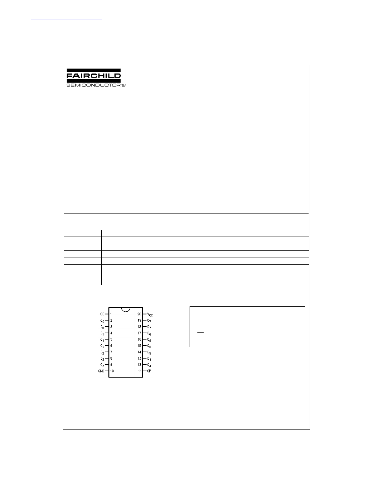
Connection Diagram Pin Descriptions
Pin Names Description
D
0–D7
CP Clock Pulse Input
OE
O
0–O7
Data Inputs
3-STATE Output Enable Input
3-STATE Outputs
FACT, Q u i et Serie s, FACT Quiet Series, and GT O are trademarks of Fairchild Semiconductor Corporation.
© 1999 Fairchild Semiconductor Corporation DS010238 www.fairchildsemi.com

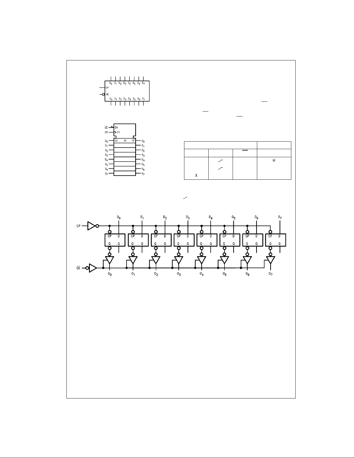
Logic Symbols
74ACQ374 • 74ACTQ374
Logic Diagram
IEEE/IEC
Functional Description
The ACQ/ACTQ374 consists of eight edge-trigger ed flipflops with individual D- type inputs and 3-STATE true outputs. The buffered clock a nd buffered Output Enable a re
common to all flip-flops. The eight flip-flops will store the
state of their individ ual D-type inputs that mee t the setup
and hold time requirements on the LOW-to-HIGH Clock
(CP) transition. With the Output Enable (OE
contents of the eight flip-flops are avai lable at th e outputs.
When the OE
ance state. Operation of the OE
state of the flip-flops.
is HIGH, the outputs go to the high imped-
input does not affect the
) LOW, the
Truth Table
Inputs Outputs
D
n
H
L
XXH Z
H = HIGH Voltage Level
L = LOW Voltage Level
X = Immaterial
Z = High Impedance
= LOW-to-HIGH Transition
CP OE O
LH
LL
n
Please note that this diagram is provided only for the understanding of logic operations and should not be used to estimate propagation delays.
www.fairchildsemi.com 2

Absolute Maximum Ratings(Note 1) Recommended Operating
Supply Voltage (VCC) −0.5V to +7.0V
DC Input Diode Current (I
V
= −0.5V −20 mA
I
= VCC + 0.5V +20 mA
V
I
DC Input Voltage (V
DC Output Diode Current (I
= −0.5V −20 mA
V
O
V
= VCC + 0.5V +20 mA
O
DC Output Voltage ( V
)
IK
) −0.5V to VCC + 0.5V
I
)
OK
) −0.5V to VCC + 0.5V
O
DC Output Source
or Sink Current (I
DC V
or Ground Current
CC
per Output Pin (I
Storage Temperature (T
) ±50 mA
O
or I
CC
) ±50 mA
GND
) −65°C to +150°C
STG
DC Latch-Up Source or Sink Current ±300 mA
Junction Temperature (T
)
J
PDIP 140°C
Conditions
Supply Voltage (V
ACQ 2.0V to 6.0V
ACTQ 4.5V to 5.5V
Input Voltage (V
Output Voltage (VO)0V to V
Operating Temperature (TA) −40°C to +85°C
Minimum Input Edge Rate ∆V/∆t
ACQ Devices
V
from 30% to 70% of V
IN
VCC @ 3.0V, 4.5V, 5.5V 125 mV/ns
Minimum Input Edge Rate ∆V/∆t
ACTQ devices
V
from 0.8V to 2.0V
IN
@ 4.5V, 5.5V 125 mV/ns
V
CC
Note 1: Absolute max imum ratings are those values beyond which damage
to the device may occu r. The databook spe cificatio ns shou ld be met, w ithout exception, to ensure that the system de sign is relia ble over its p ower
supply, temperature, and output/input loading variables. Fairchild does not
recommend operation of FACT circuits outside datab ook s pecifications.
)
CC
)0V to V
I
CC
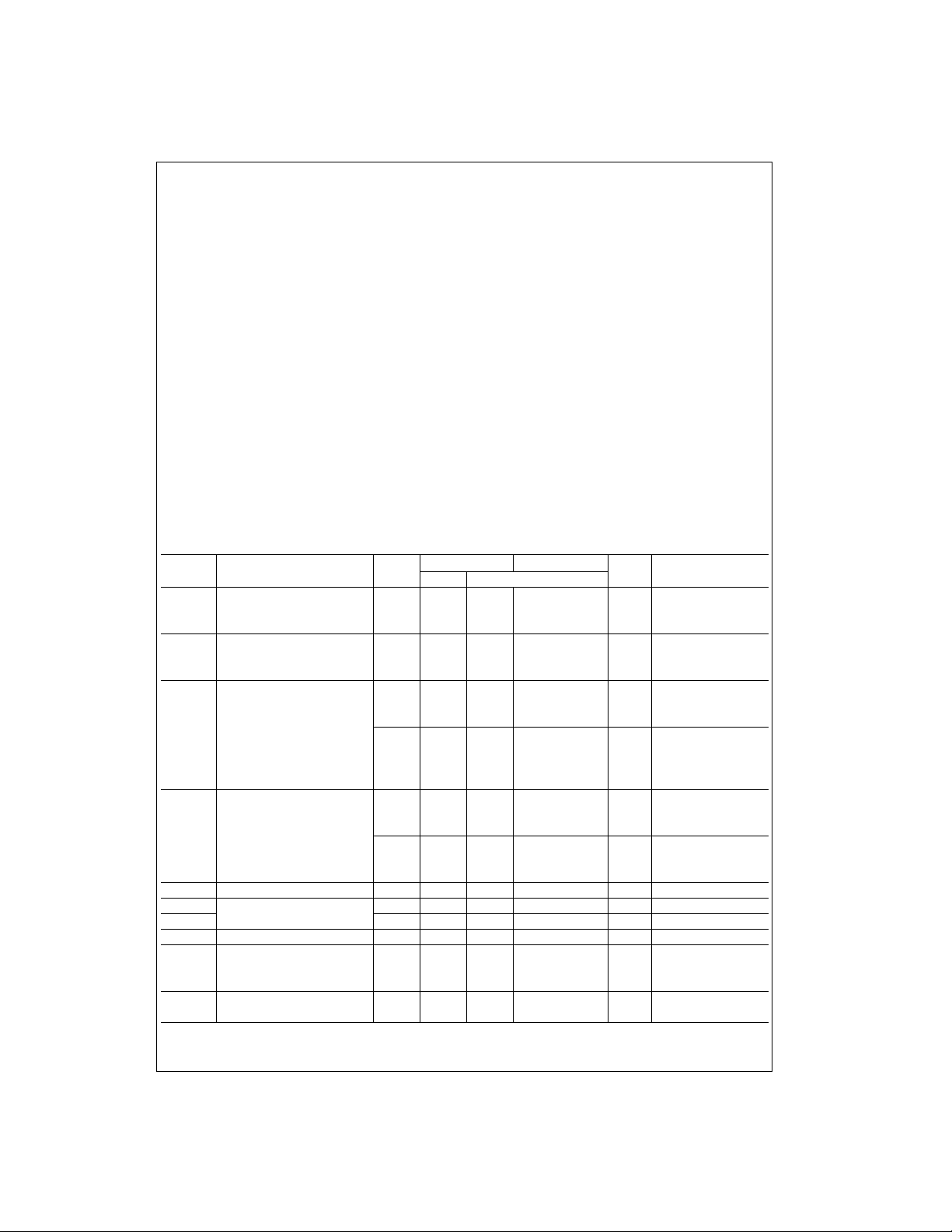
DC Electrical Characteristics for ACQ
V
Symbol Parameter
V
IH
V
IL
V
OH
V
OL
IIN (Note 4) Maximum Input Leakage Current 5.5 ±0.1 ±1.0 µAVI = VCC, GND
I
OLD
I
OHD
I
CC
I
OZ
V
OLP
Minimum HIGH Level 3.0 1.5 2.1 2.1 V
Input Voltage 4.5 2.25 3.15 3.15 V or VCC − 0.1V
Maximum LOW Level 3.0 1.5 0.9 0.9 V
Input Voltage 4.5 2.25 1.35 1.35 V or VCC − 0.1V
Minimum HIGH Level 3.0 2.99 2.9 2.9
Output Voltage 4.5 4.49 4 .4 4.4 V I
Maximum LOW Level 3.0 0.002 0.1 0.1
Output Voltage 4.5 0.001 0.1 0.1 V I
Minimum Dynamic 5.5 75 mA V
Output Current (Note 3) 5.5 −75 mA V
(Note 4) Maximum Quiescent Supply Current 5.5 4.0 40.0 µAVIN = VCC or GND
Maximum 3-STATE VI (OE) = VIL, V
Leakage Current 5.5 ±0.25 ±2.5 µAVI = VCC, GND
Quiet Output 5.0 1.1 1.5 V Figure 1, Figure 2
Maximum Dynamic V
OL
CC
(V) Typ Guaranteed Limits
5.5 2.75 3.85 3.85
5.5 2.75 1.65 1.65
5.5 5.49 5.4 5.4
3.0 2.56 2.46 IOH = −12 mA
4.5 3.86 3.76 V I
5.5 4.86 4.76 I
5.5 0.001 0.1 0.1
3.0 0.36 0.44 IOL = 12 mA
4.5 0.36 0.44 V IOL = 24 mA
5.5 0.36 0.44 IOL = 24 mA (Note 2)
TA = +25°CTA = −40°C to +85°C
Units Conditions
= 0.1V
OUT
= 0.1V
OUT
= −50 µA
OUT
VIN = VIL or V
= −24 mA
OH
= −24 mA (Note 2)
OH
= 50 µA
OUT
= 1.65V Max
OLD
= 3.85V Min
OHD
VO = VCC, GND
(Note 5)(Note 6)
74ACQ374 • 74ACTQ374
CC
CC
IH
IH
3 www.fairchildsemi.com

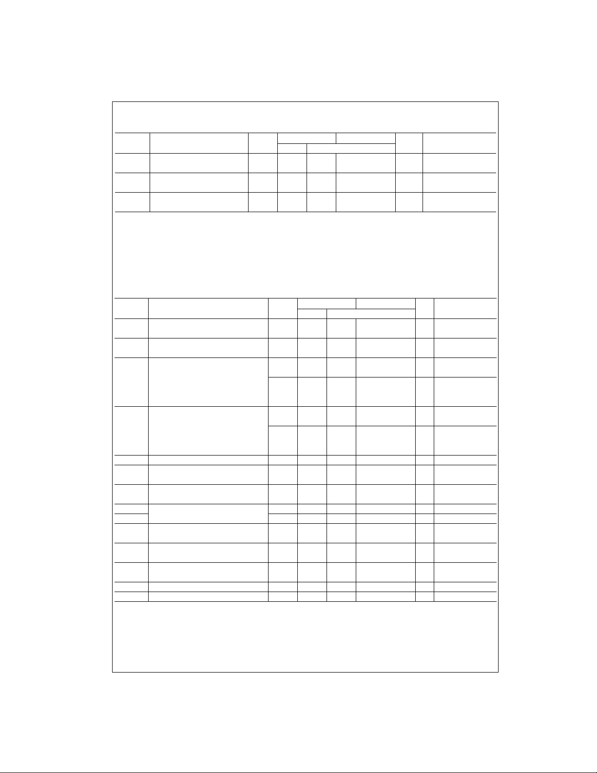
DC Electrical Characteristics for ACQ (Continued)
V
Symbol Parameter
V
OLV
V
IHD
Quiet Output 5.0 −0.6 −1.2 V Figure 1, Figure 2
Minimum Dynamic V
OL
Minimum HIGH Level
Dynamic Input Voltage
V
ILD
Maximum LOW Level
Dynamic Input Voltage
Note 2: All outputs loaded; thresholds on input associated with output under test.
74ACQ374 • 74ACTQ374
Note 3: Maximum test dura tio n 2. 0 ms, one output loaded at a time.
and ICC @ 3.0V are guaranteed to be less than or eq ual to the respective lim it @ 5. 5V VCC.
Note 4: I
IN
Note 5: DIP Package .
Note 6: Max number of output s d ef i ned as (n). Data inputs are driven 0V to 5V. One output @ GND .
Note 7: Max number of data inputs (n) switching. (n−1) inputs switching 0V to 5V (ACQ). Input-under-test switching: 5V to threshold (V
0V to threshold (V
), f = 1 MHz.
IHD
CC
(V) Typ Guaranteed Limits
5.0 3.1 3.5 V (Note 5)(Note 7)
5.0 1.9 1.5 V (Note 5)(Note 7)
TA = +25°CTA = −40°C to +85°C
Units Conditions
(Note 5)(Note 6)
DC Electrical Characteristics for ACTQ
V
Symbol Parameter
V
IH
Minimum HIGH Level 4.5 1.5 2.0 2.0
CC
(V) Typ Guaranteed Limits
Input Voltage 5.5 1.5 2.0 2.0 or VCC − 0.1V
V
IL
Maximum LOW Level 4.5 1.5 0.8 0.8
Input Voltage 5.5 1.5 0.8 0.8 or V
V
OH
Minimum HIGH Level 4.5 4.49 4.4 4.4
Output Voltage 5.5 5.49 5.4 5.4
4.5 3.86 3.76 V IOH = −24 mA
5.5 4.86 4.76 I
V
OL
Maximum LOW Level 4.5 0.001 0.1 0.1
Output Voltage 5.5 0.001 0.1 0.1
4.5 0.36 0.44 V IOL = 24 mA
5.5 0.36 0.44 IOL = 24 mA (Note 8)
I
(Note 4) Maximum Input Leakage Current 5.5 ±0.1 ±1.0 µAV
IN
I
OZ
I
CCT
I
OLD
I
OHD
I
CC
(Note 4) Supply Current or GND
V
OLP
V
OLV
V
IHD
V
ILD
Note 8: All outputs loaded; thresholds on input associated with output under test.
Note 9: Maximum test dura tio n 2. 0 ms, one output loaded at a time.
Note 10: DIP package.
Note 11: Max number of outputs defined as (n). Data inputs are driven 0V to 3V. One output @ GND
Note 12: Max number of data inp ut s (n) s w it c hing. (n−1) inputs sw it c hing 0V to 3V (ACTQ). In put -under-test switching: 3V to threshold (V
0V to threshold (V
Maximum 3-STATE
Current VO = VCC, GND
Maximum
ICC/Input (Note 4)
5.5 ±0.25 ±2.5 µA
5.5 0.6 1.5 mA V
Minimum Dynamic 5.5 75 mA V
Output Current (Note 8) 5.5 −75 mA V
Maximum Quiescent
Quiet Output
Maximum Dynamic V
Quiet Output
Minimum Dynamic V
OL
OL
5.5 4.0 40.0 µA
5.0 1.1 1.5 V
5.0 −0.6 −1.2 V
Minimum HIGH Level Dynamic Input Voltage 5.0 1.9 2.2 V (Note 10)(Note 12)
Maximum LOW Level Dynamic Input Voltage 5.0 1.2 0.8 V (Note 10)(Note 12)
), f = 1 MHz.
IHD
TA = +25°CTA = −40°C to +85°C
Units Conditions
V
V
VI
VI
),
ILD
V
= 0.1V
OUT
V
= 0.1V
OUT
− 0.1V
CC
= −50 µA
OUT
VIN = VIL or V
OH
OUT
VIN = VIL or V
= VCC, GND
I
VI = VIL, V
= VCC − 2.1V
I
OLD
OHD
VIN = V
IH
= −24 mA (Note 8)
= 50 µA
IH
IH
= 1.65V Max
= 3.85V Min
CC
Figure 1, Figure 2
(Note 10)(Note 11)
Figure 1, Figure 2
(Note 10)(Note 11)
),
ILD
www.fairchildsemi.com 4
 Loading...