Fairchild 74AC74 service manual

November 1988
Revised February 2005
74AC74 • 74ACT74
Dual D-Type Positive Edge-Triggered Flip-Flop
74AC74 • 74ACT74 Dual D-Type Positive Edge-Triggered Flip-Flop
General Description
The AC/ACT74 is a dual D-type flip-flop with Asynchronous
Clear and Set inputs and co mplementary (Q, Q
Information at the inpu t is tr ansferr ed to th e outp uts on t he
positive edge of the clock pul se. Cl ock tr iggering occurs at
a voltage level of the clock pulse and is not directly related
to the transition time of the positive- going pulse. After the
Clock Pulse input threshold voltage has been passed, the
Data input is locked out an d i nf orm atio n p resent will not be
transferred to the outp uts until the next rising edge of t he
Clock Pulse input.
Asynchronous Inputs:
LOW input to S
LOW input to C
Clear and Set are independent of clock
Simultaneous LOW on C
HIGH
(Set) sets Q to HIGH level
D
(Clear) sets Q to LOW level
D
and SD makes both Q and Q
D
) outputs.
Features
■ I
reduced by 50%
CC
■ Output source/sink 24 mA
■ ACT74 has TTL-compatible inputs
Ordering Code:
Order Number
74AC74SC M14A 14-Lead Small Outline Integrated Circuit (SOIC), JEDEC MS-012, 0.150" Narrow
74AC74SC_NL
(Note 1)
74AC74SJ M14D Pb-Free 14-Lead Small Outline Package (SOP), EIAJ TYPE II, 5.3mm Wide
74AC74MTC MTC14 14-Lead Thin Shrink Small Outline Package (TSSOP), JEDEC MO-153, 4.4mm Wide
74AC74MTCX_NL
(Note 2)
74AC74PC N14A 14-Lead Plastic Dual-In-Line Package (PDIP), JEDEC MS-001, 0.300” Wide
74ACT74SC M14A 14-Lead Small Outline Integrated Circuit (SOIC), JEDEC MS-012, 0.150" Narrow
74ACT74SC_NL
(Note 1)
74ACT74SJ M14D Pb-Free 14-Lead Small Outline Package (SOP), EIAJ TYPE II, 5.3mm Wide
74ACT74SJX_NL
(Note 2)
74ACT74MTC MTC14 14-Lead Thin Shrink Small Outline Package (TSSOP), JEDEC MO-153, 4.4mm Wide
74ACT74PC N14A 14-Lead Plastic Dual-In-Line Package (PDIP), JEDEC MS-001, 0.300” Wide
Device also availab le in Tape and Reel. Specify by appending suffix let te r “X” to the ordering code .
Pb-Free package per JECED J-STD-020B.
Note 1: “_NL” indicates lead-free product (per JEDEC J-STD-020B).
Note 2: “_NL” indicates lead-free product (per JEDE C J -ST D -020B). Device is av ailable in Tape and Reel only.
Package
Number
M14A Pb-Free 14-Lead Small Outline Integrated Circuit (SOIC), JEDEC MS-012, 0.150" Narrow
MTC14 Pb-Free 14-Lead Thin Shrink Small Outline Package (TSSOP), JEDEC MO-153, 4.4mm
Wide
M14A Pb-Free 14-Lead Small Outline Integrated Circuit (SOIC), JEDEC MS-012, 0.150" Narrow
M14D Pb-Free 14-Lead Small Outline Package (SOP), EIAJ TYPE II, 5.3mm Wide
Package Descript ion
¥
is a trademark of Fairchild Semiconductor Corporation.
FACT
© 2005 Fairchild Semiconductor Corporation DS009920 www.fairchildsemi.com

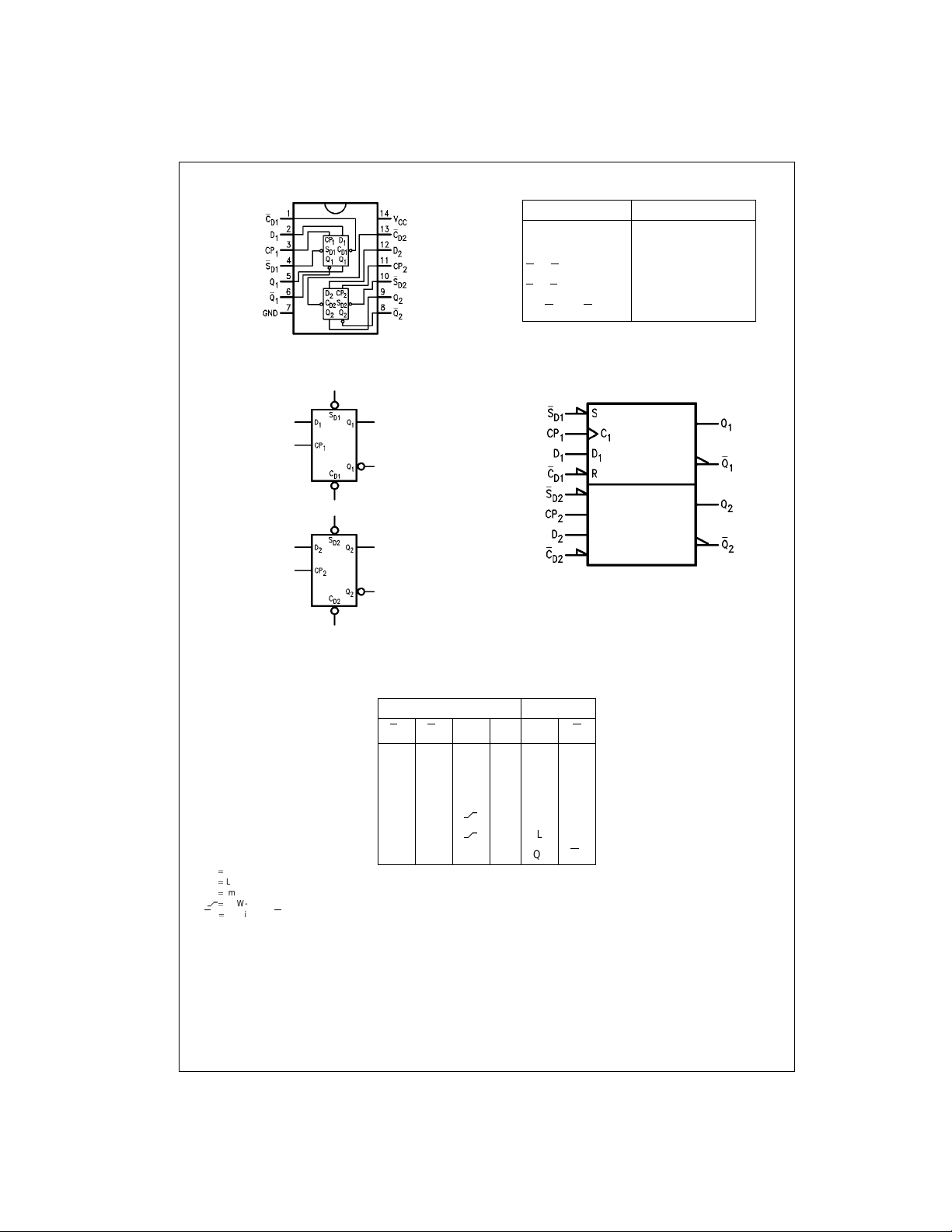
Connection Diagram Pin Descriptions
Pin Names Description
, D
D
1
2
CP
, CP
1
2
, C
C
D1
D2
, S
S
D1
D2
74AC74 • 74ACT74
Q
, Q1, Q2, Q
1
2
Data In puts
Clock Pulse Inputs
Direct Clear Inputs
Direct Set Inputs
Outputs
Logic Symbols
Truth Table
(Each Half)
S
D
LHXXHL
HLXXLH
LLXXHH
HH
HH
H HIGH Voltage Level
LOW Voltage Level
L
X
Immaterial
LOW-to-HIGH Clock Transition
(Q0) Previous Q (Q) before LOW-to-HIGH Transition of Clock
Q
0
HHLXQ
Inputs Outputs
CDCP D Q Q
HH L
LLH
0
IEEE/IEC
Q
0
www.fairchildsemi.com 2

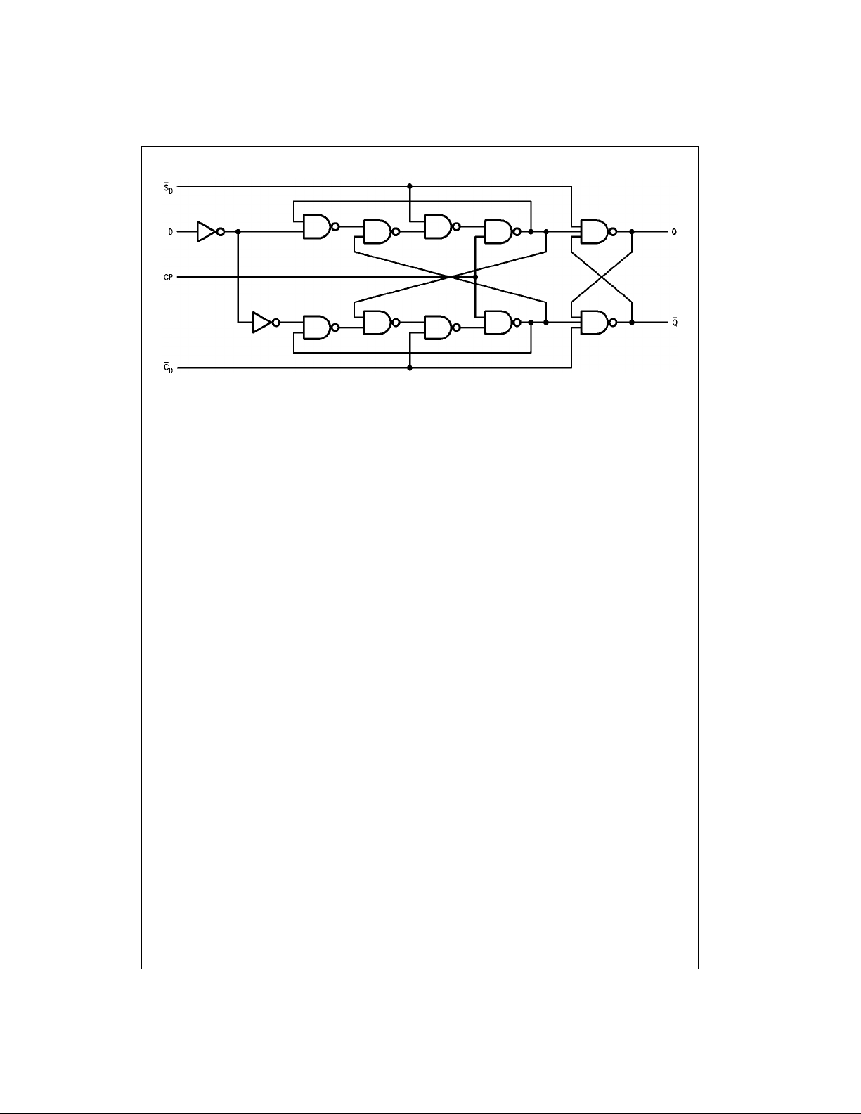
Logic Diagram
Please note that this diagram is provided only for the understanding of logic operations and should not be used to estimate propagation delays.
74AC74 • 74ACT74
3 www.fairchildsemi.com
 Loading...