Fairchild 74AC574 service manual

74AC574 • 74ACT574
Octal D-Type Flip-Flop with 3-STATE Outputs
74AC574 • 74ACT574 Octal D-Type Flip-Flop wit h 3-STATE Outputs
September 1988
Revised March 2005
General Description
The AC/ACT574 is a high-speed , low power oc tal flip-flop
with a buffered common C lock (CP) and a buffered com mon Output Enable (OE
D-type inputs is stored in the flip-flops on the LOW-to-HIGH
Clock (CP) transition.
The AC/ACT574 is functionally identical to the AC /ACT3 74
except for the pinouts.
). The information presented to the
Features
■ I
and IOZ reduced by 50%
CC
■ Inputs and outputs on opposite sides of package
allowing easy interface with microprocessors
■ Useful as input or output port for microprocessors
■ Functionally identical to AC/ACT374
■ 3-STATE outputs for bus-oriented applications
■ Outputs source/sink 24 mA
■ ACT574 has TTL-compatible inputs
Ordering Code:
Order Number Package Number Package Description
74AC574SC M20B 20-Lead Small Outline Integrated Circuit (SOIC), JEDEC MS-013, 0.300" Wide
74AC574SJ M20D Pb-Free 20-Lead Small Outline Package (SOP), EIAJ TYPE II, 5.3mm Wide
74AC574MTC MTC20 20-Lead Thin Shrink Small Outline Package (TSSOP), JEDEC MO-153, 4.4mm Wide
74AC574PC N20A 20-Lead Plastic Dual-In-Line Package (PDIP), JEDEC MS-001, 0.300" Wide
74ACT574SC M20B 20-Lead Small Outline Integrated Circuit (SOIC), JEDEC MS-013, 0.300" Wide
74ACT574SJ M20D Pb-Free 20-Lead Small Outline Package (SOP), EIAJ TYPE II, 5.3mm Wide
74ACT574MTC MTC20 20-Lead Thin Shrink Small Outline Package (TSSOP), JEDEC MO-153, 4.4mm Wide
74ACT574PC N20A 20-Lead Plastic Dual-In-Line Package (PDIP), JEDEC MS-001, 0.300" Wide
Device also availab le in Tape and Reel. Specify by appending suffix let te r “X” to the ordering code .
Pb-Free package per JEDEC J-STD-020B.
¥
is a trademark of Fairchild Semiconductor Corporation.
FACT
© 2005 Fairchild Semiconductor Corporation DS009910 www.fairchildsemi.com

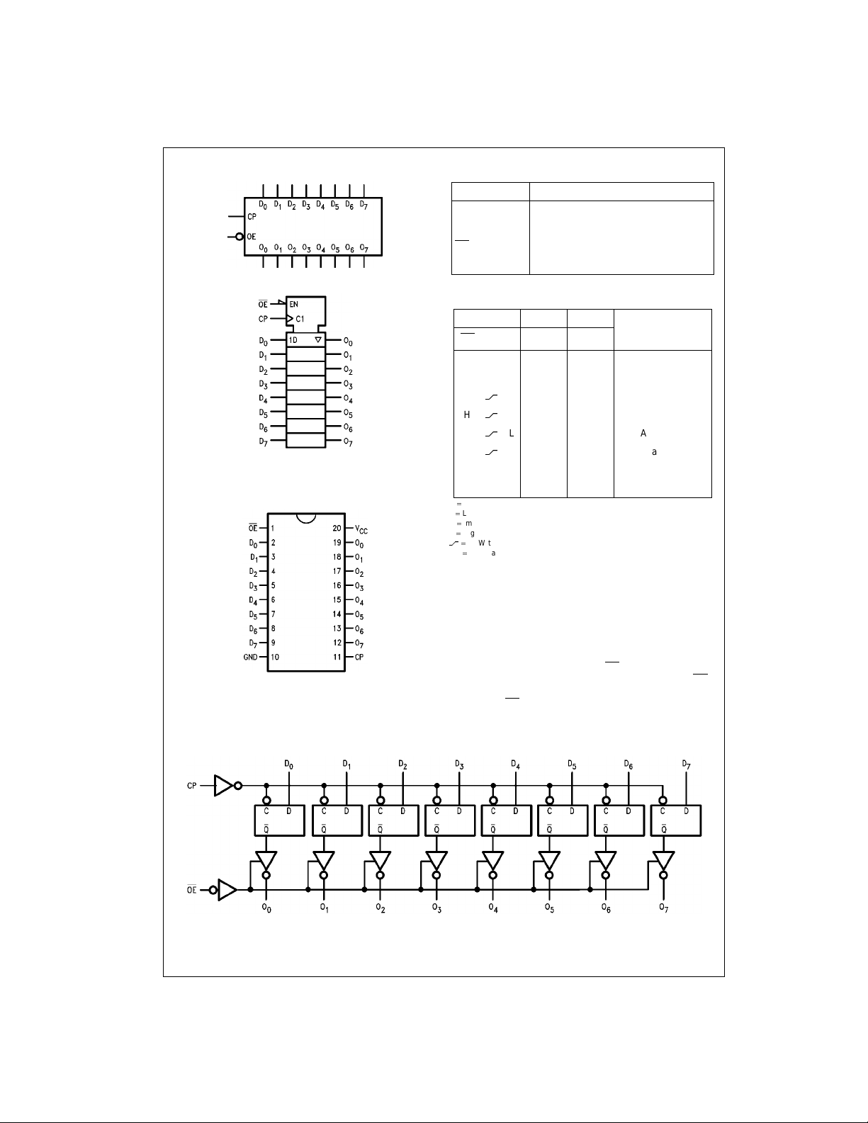
Logic Symbols
74AC574 • 74ACT574
Connection Diagram
IEEE/IEC
Pin Descriptions
Pin Names Description
D
0–D7
Data Inputs
CP Clock Pulse Input
OE
O
0–O7
3-STATE Output Enable Input
3-STATE Outputs
Function Table
Inputs Internal Outputs Function
CP D Q
OE
HHL NC Z Hold
H HH NC Z Hold
H
H
L
L
L L Z Load
H H Z Load
L L L Data Available
H H H Data Available
L H L NC NC No Change in Data
L H H NC NC No Change in Data
H HIGH Voltage Level
L
LOW Voltage Level
Immaterial
X
Z
High Impedance
LOW-to-HIGH Transition
No Change
NC
O
N
Functional Description
The AC/ACT574 consi sts of eight edge-tri ggered flip-flo ps
with individual D-type inputs and 3-STATE true outputs.
The buffered clock and buffere d Output Enable are common to all flip-flops. The eight flip-flops will store the state
of their individua l D-type inputs that meet the s etup and
hold time requirements on the LOW-to-HIGH Clock (CP)
transition. With the Ou tpu t En able ( OE
) LOW, the contents
of the eight flip-flops are available at the outputs. When OE
is HIGH, the outputs go to the high impedance state. Operation of the OE
input does not affect the state of the flip-
flops.
Logic Diagram
Please note that this diagram is provided only for the understanding of logic operations and should not be used to estimate propagation delays.
www.fairchildsemi.com 2

Absolute Maximum Ratings(Note 1) Recommended Operating
Supply Voltage (VCC)
DC Input Diode Current (I
V
0.5V 20 mA
I
VCC 0.5V
V
I
DC Input Voltage (V
DC Output Diode Current (I
0.5V 20 mA
V
O
VCC 0.5V
V
O
DC Output Voltage (V
)
IK
)
I
)
OK
)
O
0.5V to 7.0V
0.5V to VCC 0.5V
0.5V to VCC 0.5V
DC Output Source
or Sink Current (I
DC V
or Ground Current
CC
Per Output Pin (I
Storage Temperature (T
Junction Temperature (T
)
O
or I
CC
)
GND
STG
J
)
)
65q
C to 150qC
PDIP 140
20 mA
20 mA
r
50 mA
r
50 mA
Conditions
Supply Voltage (V
AC 2.0V to 6.0V
ACT 4.5V to 5.5V
Input Voltage (V
Output Voltage (VO)0V to V
Operating Temperature (TA)
Minimum Input Edge Rate (
AC Devices
V
from 30% to 70% of V
IN
VCC @ 3.3V, 4.5V, 5.5V 125 mV/ns
Minimum Input Edge Rate (
ACT Devices
V
from 0.8V to 2.0V
IN
@ 4.5V, 5.5V 125 mV/ns
V
q
C
CC
Note 1: Absolute max imum ratings are those values beyond which damage
to the device may oc cur. The databook spe cificat ions shou ld be met , without exception, to ensure that the system design is reliable over its power
supply, temperature, and output/input loading variables. Fairchild does not
recommend operation of FACT
)
CC
)0V to V
I
40q
C to 85qC
'V/'
t)
CC
'V/'
t)
¥
circuits outside databook specifications.
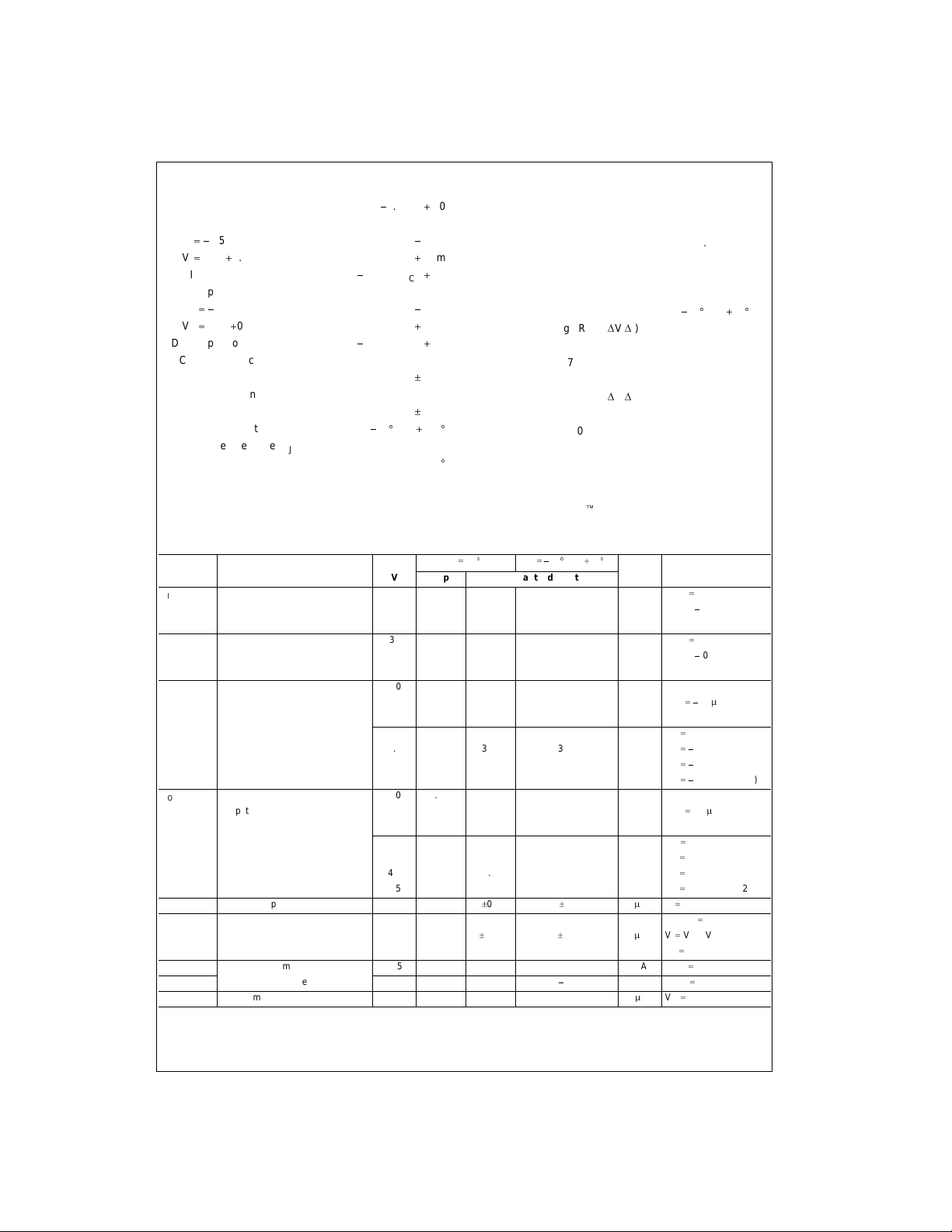
DC Electrical Characteristics for AC
V
Symbol Parameter
V
IH
V
IL
V
OH
V
OL
IIN (Note 4) Maximum Input Leakage Current 5.5
I
OZ
I
OLD
I
OHD
ICC (Note 4) Maximum Quiescent Supply Current 5.5 4.0 40.0 PAVIN VCC or GND
Note 2: All outputs loaded; thresholds on input associated with output under test.
Note 3: Maximum test duration 2.0 ms, one output loaded at a time.
Note 4: I
Minimum HIGH Level 3.0 1.5 2.1 2.1 V
Input Voltage 4.5 2.25 3.15 3.15 V or VCC 0.1V
5.5 2.75 3.85 3.85
Maximum LOW Level 3.0 1.5 0.9 0.9 V
Input Voltage 4.5 2.25 1.35 1.35 V or VCC 0.1V
Minimum HIGH Level 3.0 2.99 2.9 2.9
Output Voltage 4.5 4.49 4.4 4.4 V I
Maximum LOW Level 3.0 0.002 0.1 0.1
Output Voltage 4.5 0.001 0.1 0.1 V I
Maximum VI (OE) VIL, V
3-STATE 5.5
Leakage Current VO VCC, GND
Minimum Dynamic 5.5 75 mA V
Output Current (Note 3) 5.5
and ICC @ 3.0V are guaranteed to be less than or e qual to the respective l im it @ 5. 5V VCC.
IN
CC
(V) Typ Guaranteed Limits
5.5 2.75 1.65 1.65
5.5 5.49 5.4 5.4
3.0 2.56 2.46 VIN VIL or V
4.5 3.86 3.76 V IOH 12 mA
5.5 4.86 4.76 I
5.5 0.001 0.1 0.1
3.0 0.36 0.44 IOL 12 mA
4.5 0.36 0.44 V IOL 24 mA
5.5 0.36 0.44 IOL 24 mA (Note 2)
TA 25qCTA 40qC to 85qC
r
0.1 r1.0
r
0.25
r
2.5
75 mA V
Units Conditions
0.1V
OUT
0.1V
OUT
50 PA
OUT
IH
24 mA I
OH
IOH 24 mA (Note 2)
OUT
VIN VILor V
P
AVI VCC, GND
P
AVI VCC, V
OLD
OHD
OH
50 PA
IH
GND
1.65V
3.85V
74AC574 • 74ACT574
CC
CC
IH
3 www.fairchildsemi.com
 Loading...