74AC14, 74ACT14
Hex Inverter with Schmitt Trigger Input
74AC14, 74ACT14 — Hex Inverter with Schmitt Trigger Input
February 2011
Features
■ I
reduced by 50%
CC
■ Outputs source/sink 24mA
■ 74ACT14 has TTL-compatible inputs
General Description
The 74AC14 and 74ACT14 contain six inverter gates
each with a Schmitt trigger input. They are capable of
transforming slowly changing input signals into sharply
defined, jitter-free output signals. In addition, they have a
greater noise margin than conventional inverters.
The 74AC14 and 74ACT14 have hysteresis between the
positive-going and negative-going input thresholds (typically 1.0V) which is determined internally by transistor
ratios and is essentially insensitive to temperature and
supply voltage variations.
Ordering Information
Order
Number
74AC14SC M14A 14-Lead Small Outline Integrated Circuit (SOIC), JEDEC MS-012, 0.150" Narrow
74AC14SJ M14D 14-Lead Small Outline Package (SOP), EIAJ TYPE II, 5.3mm Wide
74AC14MTC MTC14 14-Lead Thin Shrink Small Outline Package (TSSOP), JEDEC MO-153, 4.4mm Wide
74ACT14SC M14A 14-Lead Small Outline Integrated Circuit (SOIC), JEDEC MS-012, 0.150" Narrow
74ACT14MTC MTC14 14-Lead Thin Shrink Small Outline Package (TSSOP), JEDEC MO-153, 4.4mm Wide
Device also available in Tape and Reel. Specify by appending suffix letter “X” to the ordering number.
Package
Number Package Description
©1988 Fairchild Semiconductor Corporation www.fairchildsemi.com
74AC14, 74ACT14 • Rev. 1.7.2

74AC14, 74ACT14 — Hex Inverter with Schmitt Trigger Input
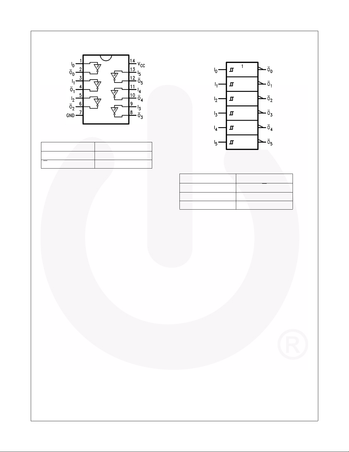
Connection Diagram
Pin Description
Pin Names Description
I
n
O
n
Inputs
Outputs
Logic Symbol
IEEE/IEC
Function Table
Input Output
AO
LH
HL
©1988 Fairchild Semiconductor Corporation www.fairchildsemi.com
74AC14, 74ACT14 • Rev. 1.7.2 2

Absolute Maximum Ratings
Stresses exceeding the absolute maximum ratings may damage the device. The device may not function or be
operable above the recommended operating conditions and stressing the parts to these levels is not recommended.
In addition, extended exposure to stresses above the recommended operating conditions may affect device reliability.
The absolute maximum ratings are stress ratings only.
Symbol Parameter Rating
V
CC
I
IK
V
I
OK
V
O
I
O
or I
I
CC
T
STG
T
Supply Voltage –0.5V to +7.0V
DC Input Diode Current
V
–0.5V –20mA
I
VCC + 1.5 +20mA
V
I
DC Input Voltage –0.5V to VCC + 1.5V
I
DC Output Diode Current
VO –0.5V –20mA
VCC + 0.5V +20mA
V
O
DC Output Voltage –0.5V to VCC + 0.5V
DC Output Source or Sink Current ±50mA
DC VCC or Ground Current per Output Pin ±50mA
GND
Storage Temperature –65°C to +150°C
Junction Temperature 140°C
J
74AC14, 74ACT14 — Hex Inverter with Schmitt Trigger Input
Recommended Operating Conditions
The Recommended Operating Conditions table defines the conditions for actual device operation. Recommended
operating conditions are specified to ensure optimal performance to the datasheet specifications. Fairchild does not
recommend exceeding them or designing to absolute maximum ratings.
Symbol Parameter Rating
V
CC
V
V
O
T
A
Supply Voltage
AC 2.0V to 6.0V
ACT 4.5V to 5.5V
Input Voltage 0V to V
I
Output Voltage 0V to V
Operating Temperature –40°C to +85°C
CC
CC
©1988 Fairchild Semiconductor Corporation www.fairchildsemi.com
74AC14, 74ACT14 • Rev. 1.7.2 3
 Loading...