Fairchild 74AC00 service manual

74AC00, 74ACT00 — Quad 2-Input NAND Gate
January 2008
74AC00, 74ACT00
Quad 2-Input NAND Gate
Features
■
I
reduced by 50%
CC
Outputs source/sink 24mA
■
■
ACT00 has TTL-compatible inputs
General Description
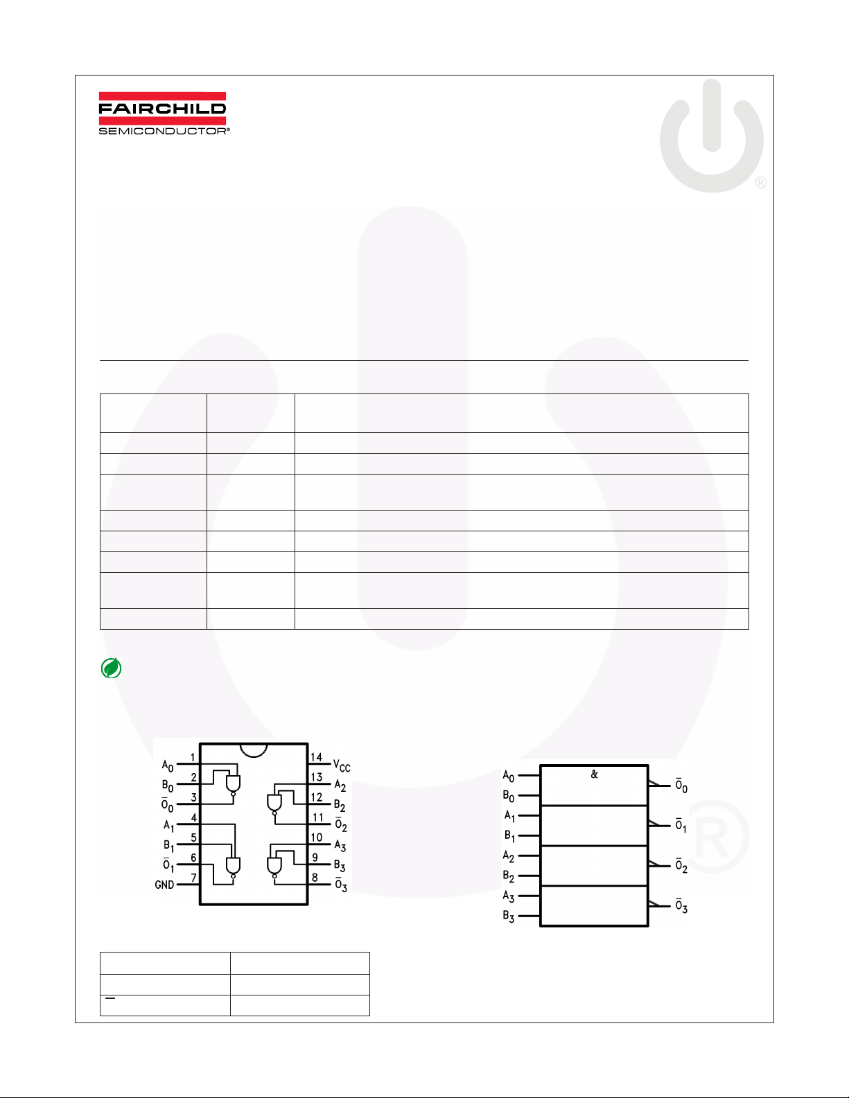
The AC00/ACT00 contains four, 2-input NAND gates.
Ordering Information
Order
Number
74AC00SC M14A 14-Lead Small Outline Integrated Circuit (SOIC), JEDEC MS-012, 0.150" Narrow
74AC00SJ M14D 14-Lead Small Outline Package (SOP), EIAJ TYPE II, 5.3mm Wide
74AC00MTC MTC14 14-Lead Thin Shrink Small Outline Package (TSSOP), JEDEC MO-153, 4.4mm
74AC00PC N14A 14-Lead Plastic Dual-In-Line Package (PDIP), JEDEC MS-001, 0.300" Wide
74ACT00SC M14A 14-Lead Small Outline Integrated Circuit (SOIC), JEDEC MS-012, 0.150" Narrow
74ACT00SJ M14D 14-Lead Small Outline Package (SOP), EIAJ TYPE II, 5.3mm Wide
74ACT00MTC MTC14 14-Lead Thin Shrink Small Outline Package (TSSOP), JEDEC MO-153, 4.4mm
74ACT00PC N14A 14-Lead Plastic Dual-In-Line Package (PDIP), JEDEC MS-001, 0.300" Wide
Device also available in Tape and Reel. Specify by appending suffix letter “X” to the ordering number.
Package
Number Package Description
Wide
Wide
All packages are lead free per JEDEC: J-STD-020B standard.
Connection Diagram
Logic Symbol
IEEE/IEC
Pin Description
Pin Names Description
A
, B
n
n
O
n
©1988 Fairchild Semiconductor Corporation www.fairchildsemi.com
74AC00, 74ACT00 Rev. 1.4.1
Inputs
Outputs

=
=
=
=
∆
∆
∆
Absolute Maximum Ratings
Stresses exceeding the absolute maximum ratings may damage the device. The device may not function or be
operable above the recommended operating conditions and stressing the parts to these levels is not recommended.
In addition, extended exposure to stresses above the recommended operating conditions may affect device reliability.
The absolute maximum ratings are stress ratings only.
Symbol Parameter Rating
V
CC
I
IK
V
I
OK
V
O
I
O
or I
I
CC
T
STG
T
Supply Voltage –0.5V to +7.0V
DC Input Diode Current
V
–0.5V –20mA
I
V
V
+ 0.5 +20mA
I
CC
DC Input Voltage –0.5V to V
I
DC Output Diode Current
V
–0.5V –20mA
O
V
V
O
+ 0.5V +20mA
CC
DC Output Voltage –0.5V to V
DC Output Source or Sink Current ±50mA
GND
DC V
or Ground Current per Output Pin ±50mA
CC
Storage Temperature –65°C to +150°C
Junction Temperature 140°C
J
CC
CC
+ 0.5V
+ 0.5V
74AC00, 74ACT00 — Quad 2-Input NAND Gate
Recommended Operating Conditions
The Recommended Operating Conditions table defines the conditions for actual device operation. Recommended
operating conditions are specified to ensure optimal performance to the datasheet specifications. Fairchild does not
recommend exceeding them or designing to absolute maximum ratings.
Symbol Parameter Rating
V
CC
V
V
O
T
A
V
/
∆
V
/
Supply Voltage
AC 2.0V to 6.0V
ACT 4.5V to 5.5V
Input Voltage 0V to V
I
Output Voltage 0V to V
Operating Temperature –40°C to +85°C
t Minimum Input Edge Rate, AC Devices:
from 30% to 70% of V
V
IN
t Minimum Input Edge Rate, ACT Devices:
from 0.8V to 2.0V, V
V
IN
,
V
CC
CC
@ 4.5V, 5.5V
CC
@ 3.3V, 4.5V, 5.5V
125mV/ns
125mV/ns
CC
CC
©1988 Fairchild Semiconductor Corporation www.fairchildsemi.com
74AC00, 74ACT00 Rev. 1.4.1 2

DC Electrical Characteristics for AC
V
Symbol Parameter
V
V
V
V
I
IN
I
OLD
I
OHD
I
CC
Minimum HIGH Level
IH
Input Voltage
Maximum LOW Level
IL
Input Voltage
Minimum HIGH Level
OH
Output Voltage
Maximum LOW Level
OL
Output Voltage
(3)
Maximum Input
Leakage Current
Minimum Dynamic
Output Current
(3)
Maximum Quiescent
Supply Current
(2)
CC
(V) Conditions
3.0 V
4.5 2.25 3.15 3.15
5.5 2.75 3.85 3.85
3.0 V
4.5 2.25 1.35 1.35
5.5 2.75 1.65 1.65
3.0 I
4.5 4.49 4.4 4.4
5.5 5.49 5.4 5.4
3.0 V
4.5 V
5.5 V
3.0 I
4.5 0.001 0.1 0.1
5.5 0.001 0.1 0.1
3.0 V
4.5 V
5.5 V
5.5 V
5.5 V
5.5 V
5.5 VIN = V
OUT
or V
OUT
or V
OUT
IN
I
OH
IN
I
OH
IN
I
OH
OUT
IN
I
OL
IN
I
OL
IN
I
OL
I
OLD
OHD
CC
CC
V
=
=
=
=
=
=
=
=
=
=
=
=
=
=
T
+25°C T
A
–40°C to +85°C
A
UnitsTyp. Guaranteed Limits
0.1V
– 0.1V
0.1V
– 0.1V
–50µA 2.99 2.9 2.9 V
V
or V
IL
,
IH
–12mA
V
or V
IL
,
IH
–24mA
V
or V
(1)
,
IH
IL
–24mA
50µA 0.002 0.1 0.1 V
V
or V
IL
,
IH
12mA
V
or V
IL
,
IH
24mA
V
or V
IL
24mA
CC
,
IH
(1)
, GND ±0.1 ±1.0 µA
= 1.65V Max. 75 mA
= 3.85V Min. –75 mA
or GND 2.0 20.0 µA
CC
1.5 2.1 2.1 V
1.5 0.9 0.9 V
2.56 2.46
3.86 3.76
4.86 4.76
0.36 0.44
0.36 0.44
0.36 0.44
=
=
=
=
=
74AC00, 74ACT00 — Quad 2-Input NAND Gate
Notes:
1. All outputs loaded; thresholds on input associated with output under test.
2. Maximum test duration 2.0ms, one output loaded at a time.
3. I
and I
IN
©1988 Fairchild Semiconductor Corporation www.fairchildsemi.com
74AC00, 74ACT00 Rev. 1.4.1 3
@ 3.0V are guaranteed to be less than or equal to the respective limit @ 5.5V V
CC
CC
.
 Loading...