1N4148WS / 1N4448WS / 1N914BWS
Small Signal Diodes
1N4148WS / 1N4448WS / 1N914BWS — Small Signal Diodes
April 2012
Features
• General Purpose Diodes
• Fast Switching Device (T
< 4.0ns)
RR
• Very Small and Thin SMD Package
• Moisture Level Sensitivity 1
• Pb-free Version and RoHS Compliant
• Matte Tin (Sn) Lead Finish
• Green Mold Compound
Absolute Maximum Ratings* T
Symbol
V
RSM
V
RRM
I
FRM
I
O
T
J
T
STG
Non-Repetitive Peak Reverse Voltage 100 V
Repetitive Peak Reverse Voltage 75 V
Repetitive Peak Forward Current 300 mA
Continuous Forward Current 150 mA
Operating Junction Temperature +150 °C
Storage Temperature Range -55 to +150 °C
Parameter Value Units
= 25°C unless otherwise noted
a
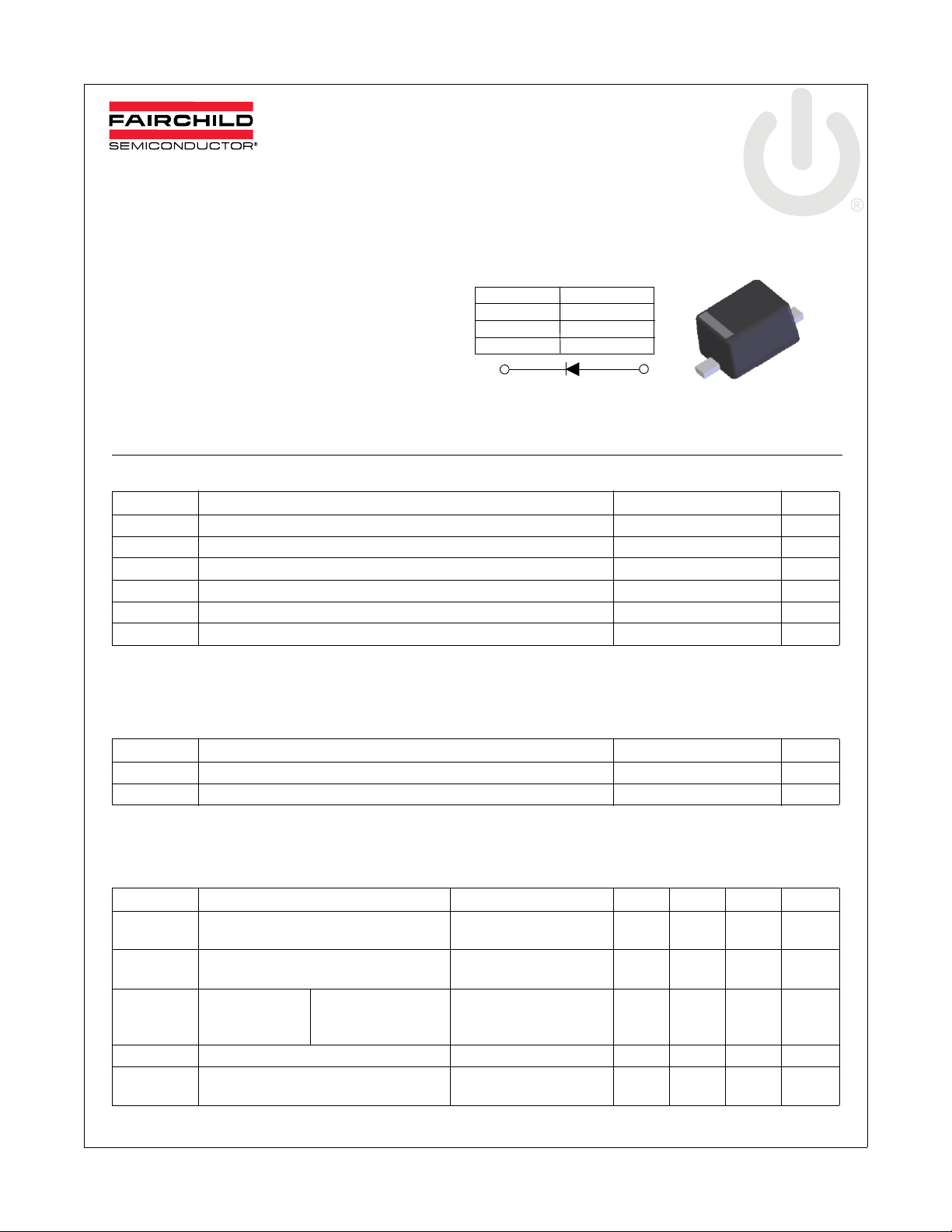
Device Marking Code
Device Type Device Marking
1N4148WS S1
1N4448WS S2
1N914BWS
1. Cathode
ELECTRICAL SYMBOL
S3
2. Anode
1
SOD-323 Flat Lead
Band Indicates Cathode
* These ratings are limiting values above which the serviceability of any semiconductor device may be impaired.
The factory should be consulted on applications involving pulsed or low duty cycle operations.
Thermal Characteristics
2
Symbol
P
D
R
θJA
Power Dissipation (TC = 25°C) 200 mW
Thermal Resistance, Junction to Ambient * 500 °C/W
Parameter Value Units
* Device mounted on FR-4 PCB minimum land pad.
Electrical Characteristics T
Symbol
BV
I
R
V
C
T
RR
© 2012 Fairchild Semiconductor Corporation www.fairchildsemi.com
1N4148WS / 1N4448WS / 1N914BWS Rev. B0 1
Breakdown Voltage IR = 100 μA
R
Reverse Current VR = 20 V
Forward Voltage 1N4448WS/914BWS
F
Diode Capacitance VR = 0, f = 1 MHz 4 pF
O
Reverse Recovery Time IF = 10 mA, IR = 60 mA,
Parameter Test Conditions
1N4148WS
1N4448WS/914BWS
= 25°C unless otherwise noted
a
= 5 μA
I
R
V
= 75 V
R
IF = 5 mA
I
= 10 mA
F
= 100 mA
I
F
= 1 mA, RL = 100 Ω
I
RR
Min. Typ. Max.
100
75
25
5
0.62 0.72
1
1
4ns
Units
V
V
nA
μA
V
V
V

Typical Performance Characteristics
[mA]
]
1N4148WS / 1N4448WS / 1N914BWS — Small Signal Diodes
0.58
0.56
0.54
0.52
0.50
0.48
Capacitance [pF]
0.46
0.44
02468101214
TA=25°C
Reverse Voltage (V)
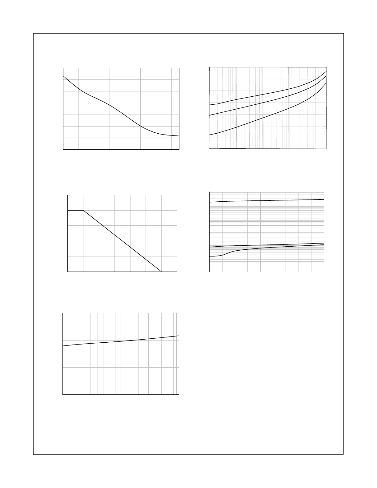
Figure 1. Total Capacitance
250
200
150
100
50
PD - Power Dissipation [mW]
0
0 25 50 75 100 125 150 175
Temperature [°C
Typical
1.2
1.0
0.8
0.6
0.4
Ta=-40°C
Ta=25°C
Ta=150°C
VF- Forward Voltage [V]
0.2
0.0
0.01 0.1 1 10 100
Forward Current, I
F
Figure 2. Forward Voltage vs. Ambient Temperature
5
10
4
10
Ta=150°C
3
10
2
10
Ta=25°C
1
10
Reverse Current [nA]
0
10
Ta=-40°C
-1
10
10 20 30 40 50 60 70 80 90 100
Reverse Voltage, VR[V]
Figure 3. Power Derating Curve Figure 4. Reverse Current vs. Reverse Voltage
170
Ta=25°C
160
150
VR - Reverse Voltage
140
110100
Reverse Current, IR[µA]
Figure 5. Reverse Voltage vs. Reverse Current
© 2012 Fairchild Semiconductor Corporation www.fairchildsemi.com
1N4148WS / 1N4448WS / 1N914BWS Rev. B0 2

Physical Dimensions
1N4148WS / 1N4448WS / 1N914BWS — Small Signal Diodes
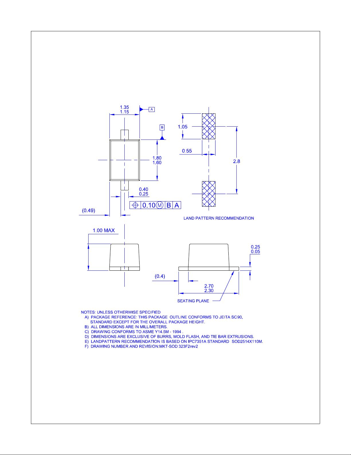
SOD-323F
Dimensions in Millimeters
© 2012 Fairchild Semiconductor Corporation www.fairchildsemi.com
1N4148WS / 1N4448WS / 1N914BWS Rev. B0 3

TRADEMARKS
®
®
®
The following includes registered and unregiste red trademarks and service ma rks, owned by Fairchild Semicondu ctor and/or its global sub sidiaries, and is not
intended to be an exhaustive list of all such trademarks.
2Cool¥
AccuPower¥
AX-CAP¥*
BitSiC¥
Build it Now¥
CorePLUS¥
CorePOWER¥
CROSSVOLT¥
CTL¥
Current Transfer Logic¥
DEUXPEED
Dual Cool™
EcoSPARK
®
®
EfficientMax¥
ESBC¥
®
Fairchild
Fairchild Semiconductor
FACT Quiet Series¥
®
FACT
®
FAST
FastvCore¥
FETBench¥
FlashWriter
®
*
FPS¥
F-PFS¥
®
FRFET
Global Power Resource
SM
GreenBridge¥
Green FPS¥
Green FPS¥ e-Series¥
Gmax¥
GTO¥
IntelliMAX¥
ISOPLANAR¥
Making Small Speakers Sound Louder
and Better™
MegaBuck¥
MICROCOUPLER¥
MicroFET¥
MicroPak¥
MicroPak2¥
®
MillerDrive¥
MotionMax¥
Motion-SPM¥
mWSaver¥
OptoHiT¥
OPTOLOGIC
OPTOPLANAR
®
®
®
PowerTrench
PowerXS™
Programmable Active Droop¥
®
QFET
QS¥
Quiet Series¥
RapidConfigure¥
¥
Saving our world, 1mW/W/kW at a time™
SignalWise¥
SmartMax¥
SMART START¥
Solutions for Your Success¥
®
SPM
STEALTH¥
SuperFET
®
SuperSOT¥-3
SuperSOT¥-6
SuperSOT¥-8
SupreMOS
®
SyncFET¥
Sync-Lock™
®
*
The Power Franchise
TinyBoost¥
TinyBuck¥
TinyCalc¥
TinyLogic
®
TINYOPTO¥
TinyPower¥
TinyPWM¥
TinyWire¥
TranSiC¥
TriFault Detect¥
TRUECURRENT
®
*
PSerDes¥
®
UHC
Ultra FRFET¥
UniFET¥
VCX¥
VisualMax¥
VoltagePlus¥
XS™
* Trademarks of System General Corporation, used under license by Fairchild Semiconductor.
DISCLAIMER
FAIRCHILD SEMICONDUCTOR RESERVES THE RIGHT TO MAKE CHANGES WITHOUT FURTHER NOTICE TO ANY PRODUCTS HEREIN TO IMPROVE
RELIABILITY, FUNCTION, OR DESIGN. FAIRCHILD DOES NOT ASSUME ANY LIABILITY ARISING OUT OF THE APPLICATION OR USE OF ANY PRODUCT
OR CIRCUIT DESCRIBED HEREIN; NEITHER DOES IT CONVEY ANY LICENSE UNDER ITS PATENT RIGHTS, NOR THE RIGHTS OF OTHERS. THESE
SPECIFICATIONS DO NOT EXPAND THE TERMS OF FAIRCHILD’S WORLDWIDE TERMS AND CON DITIONS, SPECIFICALLY THE WARRANTY THEREIN,
WHICH COVERS THESE PRODUCTS.
LIFE SUPPORT POLICY
FAIRCHILD’S PRODUCTS ARE NOT AUTHORIZED FOR USE AS CRITICAL COMPONENTS IN LIFE SUPPORT DEV ICES OR SYSTEMS WITHOUT THE
EXPRESS WRITTEN APPROVAL OF FAIRCHILD SEMICONDUCTOR CORPORATION.
As used herein:
1. Life support devices or systems are devices or systems which, (a)
are intended for surgical implant into the body or (b) support or
sustain life, and (c) whose failure to perform when properly used in
accordance with instructions for use provided in the labeling, can be
2. A critical component in any component of a life support, device, or
system whose failure to perform can be reasonably expected to
cause the failure of the life support device or system, or to affect its
safety or effectiveness.
reasonably expected to result in a significant injury of the user.
ANTI-COUNTERFEITING POLICY
Fairchild Semiconductor Corporation's An ti-Counter feiting Poli cy. Fairchi ld's An ti-Counter feiting Policy is also state d on ou r external website, w ww.fair childsemi.com ,
under Sales Support.
Counterfeiting of semiconductor parts is a grow ing problem in the industry . All manu facturers of semicon ductor pro ducts are e xp eriencing counter feiting of thei r
parts. Customers who inadvertently purch ase co unterfeit p arts ex perience many problem s such as loss of brand repu tation, substan dard performan ce, failed
applications, and increased cost o f productio n and man ufacturing delays. Fairchild is taking strong mea sures to protect oursel v es and our custome rs from the
proliferation of counterfeit parts. Fairchild strongly encourag es customers to purchase Fairchild par ts either directly from Fairchild or fr om Authorize d Fairchild
Distributors who are listed by country on our web page cited above. Products customers buy either from Fairchild directly or from Authorized Fairchild Distrib utors
are genuine parts, have full tr aceability , meet Fairchild' s quality standards for handling and storage and pr ovide a ccess to Fa irchild's full range of up-to-date technical
and product information. Fairchild and ou r Authorized Distributo rs will stan d behind all warran ties and will appropriate ly addr ess any warranty issues that may ari se.
Fairchild will not provide any w arranty coverage o r other assistance fo r parts bo ught from Unauthorized Sources. F airchild is committed to combat this global
problem and encourage our customers to do their par t in stopping this practi ce by buying direct or from au thorized distr ibutors.
PRODUCT STATUS DEFINITIONS
Definition of Terms
Datasheet Identification Product Status Definition
Advance Information Formative / In Design
Preliminary First Production
No Identification Needed Full Production
Obsolete Not In Production
Datasheet contains the design specifications for product development. Specifications may change
in any manner without notice.
Datasheet contains preliminary data; supplementary data will be published at a later date. Fairchild
Semiconductor reserves the right to make changes at any time without notice to improve design.
Datasheet contains final specifications. Fairchild Semiconductor reserves the right to make
changes at any time without notice to improve the design.
Datasheet contains specifications on a product that is discontinued by Fairchild Semiconductor.
The datasheet is for reference information only.
Rev. I61
© Fairchild Semiconductor Corporation www.fairchildsemi.com

 Loading...