

Facit 1123 User Manual
Contents
Section Page
Title & Contents (this page) 1
Notes & Signal Names 2
Block Diagram 3
Timing 4
Keyboard and OP Flag 5
Control (part 1) 6
Control (part 2) 7
Registers 8
Decimal Point Register & Q Flag 9
Arithmetic 10
Display Latch & Display 11
Power Supply 12
Timing Diagram 13
IC Pinouts & Physical Layout 14
Connectors 15
Facit 1123
Calculator
Facit 1123 Calculator
Section: Title and Contents
Page: 1 Rendition: 2014 Mar 6
This schematic has been derived through the reverse
engineering of a Facit 1123 calculator.
This is not the manufacter’s schematic, nor is it
based on the manufacturer’s schematic.
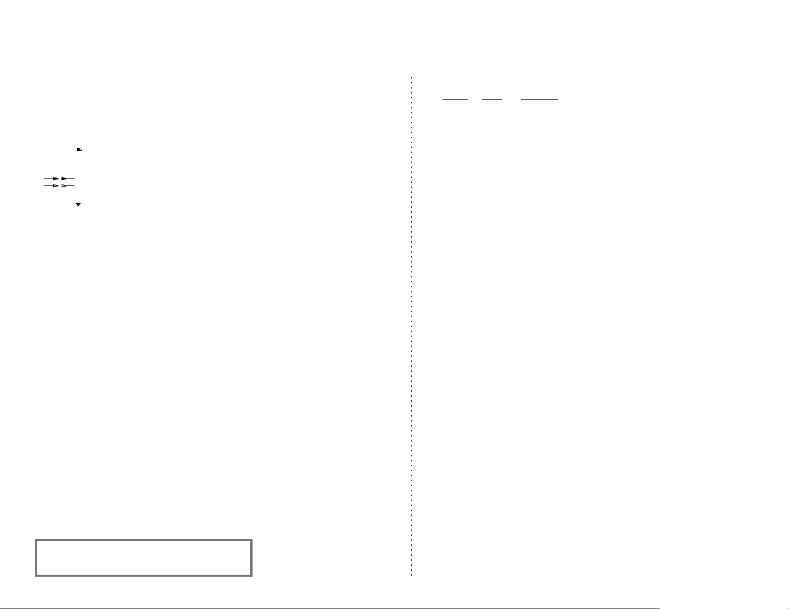
Notes
♦ IC numbering: IC
brc
where b=board, r=row, c=column. Board is 1,2 or 3 starting from the top. Row and column are counted
from top left corner of board while holding board with parts up and connector on the right. See Physical Layout page.
♦ Gate symbols and signal names are presented in accordance with:
logic 0 = GND
logic 1 = Vcc
♦ The symol
N
bpp
denotes a physical connector pin, where b =1 to 3 for the PC board connectors starting from the top, K for the
keyboard connector and R for the test/remote connector underneath the chassis, and pp=pin. Solid black end is the male side
of the connector. White end is the female side of the connector.
♦
connection between different sections.
connection within same section.
Arrows indicate direction of signal or energy flow.
♦ The symbol denotes Vcc.
♦ Capacitance in microfarads unless otherwise indicated.
♦ These drawings based on unit with Serial No.: 302.500.
♦ Drawn by bhilpert. See www.cs.ubc.ca/~hilpert/eec for additional information.
Change Log
♦ July 1996: Initial creation.
♦ 31 Oct 2004: Manual control notes added. N4 and N5 renamed to NK and NR.
OP-Cycles and Manual Control of Operations
A switch can be plugged into the remote connector (NR) to provide the ability to single-step through the major state cycles of an
operation. See the Keyboard & OP page for wiring of the switch.
An OP-cycle is a full number cycle during which processing occurs and is indicated by the OP signal. Major state transitions
occur at the end of an OP-cycle. Simple user operations such as numeral entry generate a single OP-cycle without sending P0 to
0. More complex operations requiring multiple number cyclesgenerate a first OP-cycle and send P0 to 0. Multiple OP-cycles are
subsequently generated until the operation is complete, at which time P0 returns to 1.
Enabling the MANUAL switch disables the automatic generation of OP-cycles for multi-cycle operations. In this mode, once a
multi-cycle operation has been initiated, each press of the CLE key generates a single OP-cycle, so the operation can be stepped
through one OP-cycle at a time.
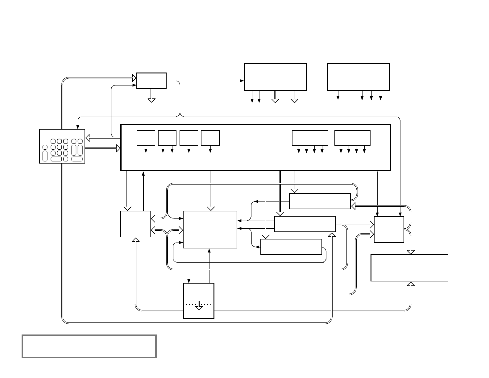
Signal Names
Section Signal Description
Timing Ø… Master timing.
Ø Master clock from which all timing is derived. This is the basic bit rate.
ØB… Bit timing.
ØD0…ØD15 Digit Timing. 16 digit intervals, ØD2–ØD15 are the displayed digit time periods;
Registers do not cycle during ØD0.
Keyboard K
…
various (unlatched) indications from the keyboard.
A 1=Add, 0=subtract.
C 1=calculation is multiply or divide, 0=add or subtract.
M 1=Multiply
D 1=Divide
N 1=Normal mode, 0=use the Z register, also associated with the decimal point.
OP OP… Operation cycle.
Control P0 state 0 of the 2-bit P state register: 1=idle, 0=calculating.
P1 – P3 the other 3 states of the P register indicating some aspect of calculation.
R0 – R3 the 4 states of the 2-bit R state register.
S
<p><r>
shorthand for states of the P and R register: S
<p><r>
= P
<p>
• R
<r>
.
DISP 1=displaying, 0=calculating , same as P0 but with additional control from
connector N5.
CY… Outputs from control to the Y register.
CX… “ the X register.
CZ… “ the Z register.
CA… “ select the source for the A input of arithmetic.
CB… “ select the source for the B input of arithmetic.
CS… “ select the arithmetic function.
CD… “ the decimal point register.
CQ… “ the Q flag.
X Register X… The operand being displayed.
X1,X2,X4,X8 BCD numerals on their way to the display.
Y Register Y… The second operand.
Y
YP1
Z Register Z The user memory.
DP Register DP… The decimal point register.
Arithmetic ASUM16 The raw digit sum from the serial adder, base 16.
ASUM10 The normalized digit sum after correcting for values between 10 and 15 inclusive.
Q Flag Q The 1-bit Q flag for catching data conditions.
Display Latch DL… Latch for numerals during the digit display interval, also used for transferring from
the DP register to the Y register.
♦ A lowercase “n” in a symbol name indicates the logical NOT operation.
♦ The character “ • ” in a symbol name indicates the logical AND operation.
♦ The character “+” in a symbol name indicates the logical OR operation.
Algorithm Notes
♦ During multiply and divide, a hex ‘F’ is placed after the LSD of one of the operands. The operand is shifted up to
the upper end of the register and the F is used to indicate where arithmetic will begin during the number cycle.
♦ During multiply and divide, the uppermost digit of the Y register is used as a digit counter to limit the multiply/divide
loop.
Facit 1123 Calculator
Section: Notes & Signal Names
Page: 2 Rendition: 2014 Mar 6
OP•Ø…
ASUM16
ASUM10
DPR In
DPR
DPR1, DPR2, DPR4, DPR8
DP0 – DP6
DPNE, DPGT, DP>6, DP<8
Q
CQ…
CA…, CB…, CS…
CX…
CY…
S23
X1, X2, X4, X8
X, X1, X2, X4, X8
Y4, Y8,
YP1YDL1, DL2, DL4, DL8
DL1, DL2, DL4
K1, K2, K4, K8
K…
P0, R0+R1
KCLR, KP
P0
DISP
Q-bit
CZ…
Z
Z Register
(56 bits)
X Register
(60 bits)
Arithmetic
Control
14 Nixie Displays
Keyboard
43210987654321.
Y Register
(60 bits)
Decimal Point
Register
(4 bits)
(decoder)
Ø
Øp
ØB
x
bit timing
ØD
x
digit timing
Timing
OP
clock rate
selection
Display Latch
(4 bits)
V
CC
logic supply
display supplies
V
+26V+70V+180
Power Supply
P State Register
(2 bits)
R State Register
(2 bits)
Facit 1123 Calculator
Section: Block Diagram
Page: 3 Rendition: 2014 Mar 6
A flag
(1 bit)
C flag
(1 bit)
N flag
(1 bit)
M/D flag
(1 bit)
AMDCNP0P1P2P3R0R1R2R356
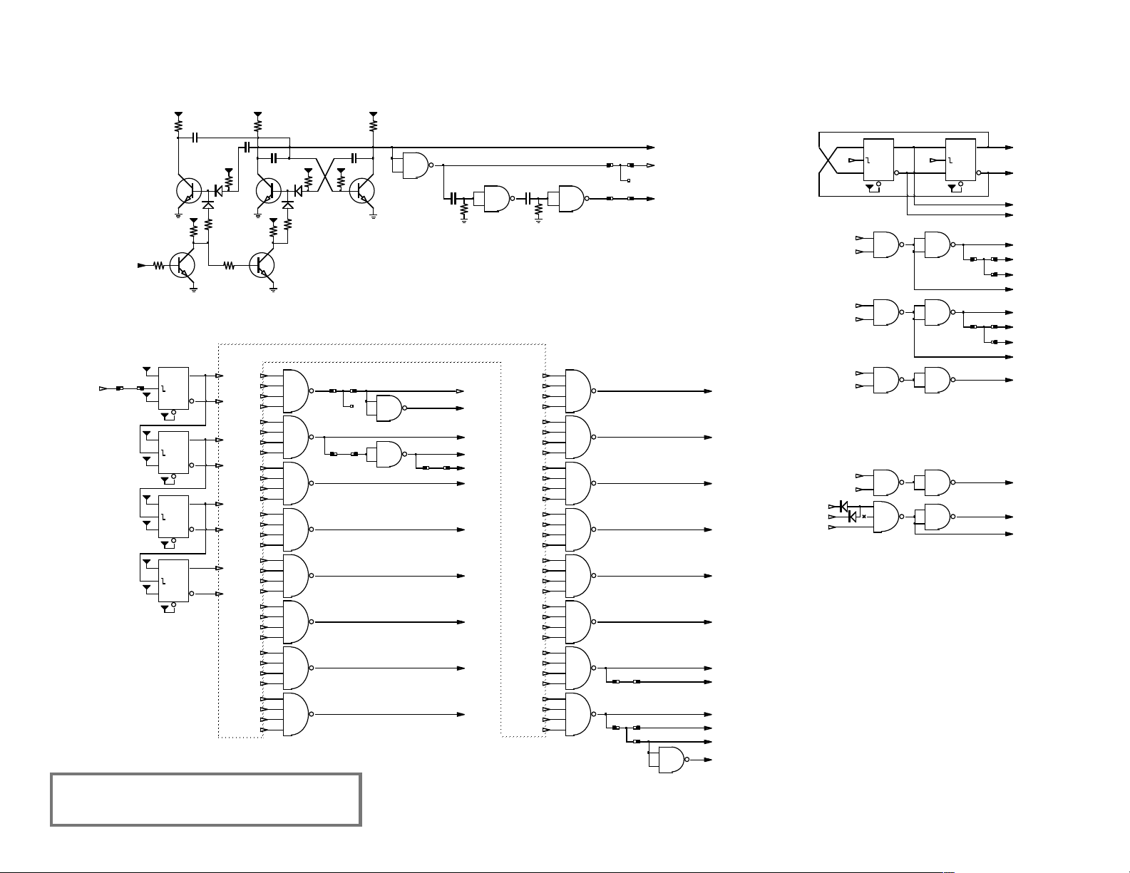
IC24841211IC24813ØB18
ØB12
nØB1
ØB1564IC22932
IC2291nØD0ØØnD0•Ø1K5K2K2K5K2K2K10K
10K
50K
30K
500pF
300pF
200pF
100pF
8910564231
20K
20K
N130
N132
nØ
to display
IC111
IC111
IC111
2SC641
2SC641
2SC641
2SC641
2SC641
300pF
300pF56
2
4391312
101156IC1624329
13
IC162
10111226
IC1514359
13
IC131
11121026
IC14134512
13
IC1411110926IC131
3
4512
13
IC1511110926IC13234512
13
IC132
111091213
IC1619101126354
12
13
11910
N110
nØD2
nØD3
nØD4
nØD5
nØD6
nØD7
nØD8
nØD9
nØD10
nØD11
nØD12
nØD13
N120
nØD14
N118
nØD1526
IC161543N108
nØD0n1n2n4n81n2n4n8n12n4n812n4n8n1n24n81n24n8n124n812
4n8n1n2n481n2n48n12n4812n48n1n2481n248n1248124891245321n12n2N117
IC152
IC152
IC121
IC121
IC122
IC122810
N231
N229
N218
N207
nØD1
N209
N219
N217
N318954IC24913118101223IC249
ØB48
ØB12
ØB24
ØB18ØØp61311ØØØB4891245324n48n8
IC142
IC142810131123
IC24711112IC24713Øp
ØB1p
ØB12314
IC237564IC247111213IC229
n(ØD0•B2)
ØD0•B2
ØD023
IC24898
IC248
10
ØB18
ØB48
nØB8
ØB8910
IC229
N2448ØD1
N254
ØB12
ØB24
ØD0
DISP
N116
N353
N252
N127
N351
N344116JKQnQnCJKQnQJKQnQJKQnQ89
10
IC370
ØD15
1JKQnQJKQnQ61
42K
Facit 1123 Calculator
Section: Timing
Page: 4 Rendition: 2014 Mar 6
nCnCnCnCnC
NR44
NR45
3×÷
N328
N325
2.2K
2.2K
10K
CE
DP×÷=–
N211CLN3350123456789RCN306
N307
N308
N309
N310
N311
N312
N313
N303
N305
N329
N333
N319
N330
N332
N321
N331
11 of
20K
12
13
IC329
11109
564
IC3188910IC3189IC3191110125
IC319432231
IC318n1n3n5n7n9n2n3n6n7n4n5n6n7n8n96
13n0n1n2n3n4n5n6n7n8n9
2.2K
10K1211138910
IC327
IC327
8
910IC328564IC328
N326
N324
N322
N32012IC310116581243n6n8n9n0
n2n4N227
N225
N223
N221K1K2K4K85IC3264238112116111213IC317
nCE
nRCnAnS
nCE
nKCLR
nKCLR111213IC3184IC329523nAnSnZA
nZS6nKMD
N323
N327
nZR
nZC
N315
N317
nZA
nZS
nZRKFMKNnKN
DISP111213IC328321IC32413101211
IC323CnCMD
CDnKCLR1234
IC323KFOP•ØD0•B4p
R19586
IC3161243
IC316AnSnAnZA564IC35498
IC35410nZA
nZS
OP•ØD0•B4p
4
IC314328111211342
IC359nSnA
nCENnN21
IC328
R0+R1
N213
N3141KP
to OP
nDnMnDnMnRC
nZC
nZR
nKRC
nKZC
nKZR
OP•ØD0•B1p
569810
IC325
S11•nQ
nKCLRnDnZS
nRC
nZC
nM
to
X Register
NK10
NK36
NK43
NK45
nP0
NK18M+M–MRMC12IC24691011ØB24
ØB48
1211IC2451313Øp56IC236498IC23610231
IC2361112
IC23613N249OPØB1p
ØD0564IC2328695
IC237569832
IC253
N203
20K
IC242121113523
IC2384IC23881098910
IC239
231
564
IC239
IC2391211
IC23913OP
ØD0•B289
IC257106
N246
nOP35
4
IC266
M5962
635
4
IC256
M5962
ØD0•B2
N263
nØD14OPN215
nOPnPDISP
to Display Latch
Øp
ØD1
N304
DISP
to Timing (clock rate)
DISP
to Keyboard
N137
N2051N256ØpØD0•B2
OP•ØD0•B4p
OP•ØD0•B1p
n(OP•ØD0•B2p)
nKCLR16JKQnQJKQnQ
N316
N366
N365
N360
N342
nP0
nOP•ØD14p
111213
IC355OPKP
NR17
NK01
NK02
NK03
NK04
NK05
NK06
NK07
NK08
NK09
NK30
NK37
NK35
NK31
NK32
NK33
NK34
NK38
NK39
NK??
NK??
Facit 1123 Calculator
Section: Keyboard & OP Flag
Page: 5 Rendition: 2014 Mar 6
11 of
20KnCnC
MANUAL
NORMAL
Controller / Monitor Unit
(see Notes page)
NR29
nMANUAL
NR27
NR10
NR01
NR02
NR03
NR04
NR05
NR06
NR07
NR08
NR09
NR30
NR37
NR35
NR33
NR34
NR31
NR32
NR38
NR39
NR??
NR??
NR36
620
BUSY
NR18
nP0
Use high efficiency
LED run at low
current (~ 3mA) to
minimise drain on
source.
NR44ØNR45
nØD0
NR27
nOP
NR19XNR43
XØENB
NR42
ASUM16
TEST
POINTS1211654IC362P1Q
 Loading...