

Page 1
User Guide — EP9134_UG V0.2
深圳诗普睿
13928451944
4 Ports HDMI 1.3 Splitter
EP9134
User Guide
V0.2
Revised: Mar. 14, 2008
Original Release Date: Aug. 27, 2007
Explore
Explore reserves the right to make changes without further notice to any products herein to improve reliability, function or design.
Explore does not assume any liability arising out of the application or use of any product or circuit described herein; neither does it
convey any license under its patent rights nor the rights of others. Explore products are not designed, intended, or authorized for use
as components in systems intended for surgical implant into the body, or other applications intended to support or sustain life, or for
any other application in which the failure of the Explore product could create a situation where personal injury or death may occur.
Should Buyer purchase or use Explore products for any such unintended or unauthorized application, Buyer shall indemnify and hold
Explore and its officers, employees, subsidiaries, affiliates, and distributors harmless against all claims, costs, damages, and expenses,
and reasonable attorney fees arising out of, directly or indirectly, any claim of personal injury or death associated with such unintended
or unauthorized use, even if such claim alleges that Explore was negligent regarding the design or manufacture of the part.
Explore Confidential Proprietary
NON-DISCLOSURE AGREEMENT REQUIRED
1
Page 2
User Guide — EP9134_UG V0.2
深圳诗普睿
13928451944
Revision History
Version
Number
0.0 Aug/27/2007 Jerry Chen Initial Version
0.1 Jan/11/2008 Ether Lai Revised Version
0.2 Mar/14/2008 Ether Lai Revise Register Description; Change package type;
Revision
Date
Author Description of Changes
2
Explore Confidential Proprietary
NON-DISCLOSURE AGREEMENT REQUIRED
Page 3
User Guide — EP9134_UG V0.2
深圳诗普睿
13928451944
Section 1 Introduction
1.1 Overview
The EP9134 is a 4-Port DVI/HDMI splitter with integrated HDCP decryption/encryption engines and is
compliant with HDMI Rev 1.3b and HDCP Rev 1.2 specifications. The EP9134 receives DVI/HDMI
inputs, process HDCP decryption and encryption and transmits the data to 4 DVI/HDMI ports. The chip
uses an external EE to store the encrypted HDCP receiver/transmitter keys.
1.2 Features
• DVI Specification 1.0 Compliant
• HDMI Specification 1.3b Compliant
• Integrated HDCP decryption/encryption engines which are compliant with HDCP Rev 1.1
specification
• Encrypted HDCP keys store in external serial EE
• Wide Frequency Range: 25MHz - 225MHz
• Support 12-bit Deep Color up to 1080p
• Supports 1 DVI/HDMI input port and 4 DVI/HDMI output ports
• Supports conversion of HDMI signaling to DVI signaling
• Supports HDCP Repeater
• Cascadable to make more than 4 output ports
• 128-Pin HQFP (Pb-Free)
3
Explore Confidential Proprietary
NON-DISCLOSURE AGREEMENT REQUIRED
Page 4
User Guide — EP9134_UG V0.2
深圳诗普睿
13928451944
4
Explore Confidential Proprietary
NON-DISCLOSURE AGREEMENT REQUIRED
Page 5
Section 2 Overview
深圳诗普睿
13928451944
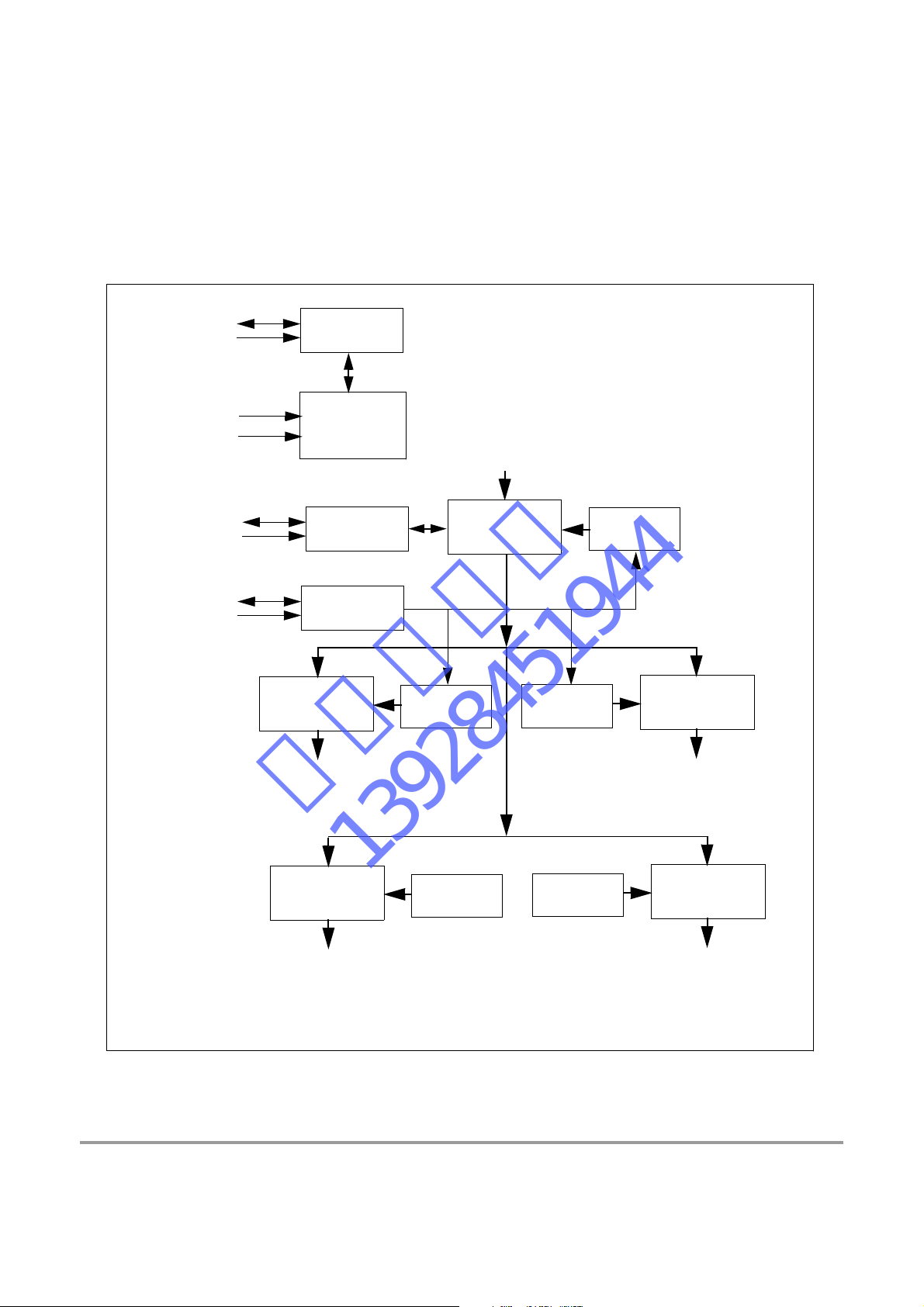
2.1 Block Diagram
User Guide — EP9134_UG V0.2
SDA3
SCL3
EXT_RSTb
EXT_SWING
SDA1
SCL1
SDA2
SCL2
IIC Slave
Registers
&
Logics
IIC Slave
IIC Master
DVI/HDMI
Transmitter
Figure 2-1 Block Diagram
RX0+/-
RX1+/-
RX2+/-
RXC+/-
DVI/HDMI
Receiver
HDCP Keys
HDCP Keys
HDCP Keys
DVI/HDMI
Transmitter
TX00+/-
TX10+/-
TX20+/-
TXC0+/-
DVI/HDMI
Transmitter
TX02+/-
TX12+/-
TX22+/-
TXC0+/-
Explore Confidential Proprietary
NON-DISCLOSURE AGREEMENT REQUIRED
HDCP Keys
HDCP Keys
TX01+/-
TX11+/-
TX21+/-
TXC1+/-
DVI/HDMI
Transmitter
TX03+/-
TX13+/-
TX23+/-
TXC1+/-
5
Page 6
User Guide — EP9134_UG V0.2
深圳诗普睿
13928451944
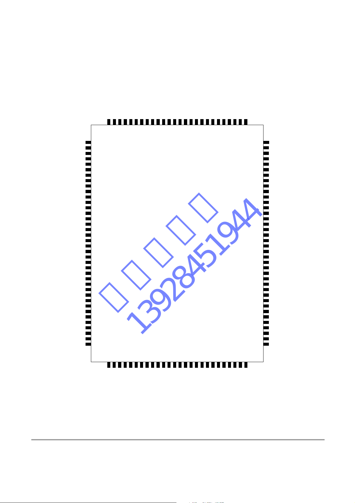
2.2 Pin Diagram
AVS S
TXC2+ 3
AVDD 4
TX02- 5
TX02+ 6
AVSS 7
AVSS 8
TX12- 9
TX12+ 10
AVD D 11
TX22- 12
TX22+ 13
AVS S 14
AVS S 15
VDD18 16
VDD18 17
VSS 18
VSS 19
A0 20
A1 21
A2 22
EXT_RSTb 23
VDD18 24
VSS 25
SCL1 26
SDA1 27
SCL2 28
SDA2 29
VDDE 30
VSSE 31
reserved 32
reserved 33
SCL3 34
SDA3 35
V_OUT 36
HTPLG0 37
HTPLG1 38
Figure 2-2
PVSS
PVDD
AVSS
PVDD
EXT_SWING23
124
126
127
128
125
1
2TXC2-
PVSS
123
AVSS
122
AVS S
121
TX23+
120
Pin Diagram
TX13+
AVDD
AVD D
TX23-
116
118
117
119
TX13-
115
AVSS
114
AVS S
113
TX03+
112
TX03-
111
AVDD
110
AVDD
109
TXC3+
108
TXC3-
107
AVS S
106
AVSS
105
_AVSS
104
_AVSS
103
_AVSS102
_AVSS101
_AVSS100
_AVSS99
_AVSS98
AVS S97
RX2+96
RX2-95
AVD D94
RX1+93
RX1-92
AVS S91
AVD D90
AVS S
89
RX0+
88
87
RX0AVS S
86
85
RXC+
RXC-
84
83
AVD D
82
EXT_RES
81
PVDD
80
PVSS
AVS S
79
78
AVSS
TX20+
77
TX20-
76
AVDD
75
TX10+74
73
TX10AVSS
72
71
AVSS
70 TX00+
69 TX0068 AVDD
67 TXC0+
66 TXC065 AVSS
41
40
39
VDD18
HTPLG3
HTPLG2
6
45
47
50
51
44
43
42
VSS
VSS
AVSS
VDD18
49
48
46
AVSS
TXC1-
TXC1+
AVDD
52
AVSS
TX01-
TX01+
Explore Confidential Proprietary
53
54
AVSS
TX11-
NON-DISCLOSURE AGREEMENT REQUIRED
55
TX11+
58
TX21+
59
AVSS
61
60
63
64
62
AVSS
AVS S
PVDD
PVSS
EXT_SWING01
57
56
TX21-
AVD D
Page 7
User Guide — EP9134_UG V0.2
深圳诗普睿
13928451944
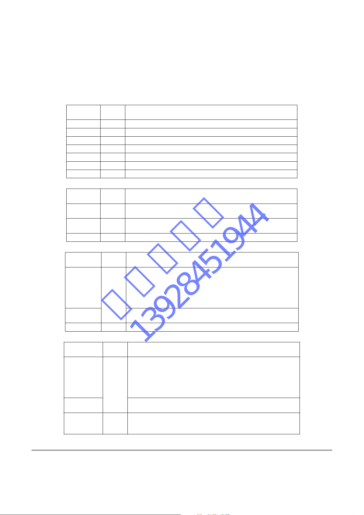
2.3 Pin Description
Unless otherwise stated, unused input pins must be tied to ground, and unused output pins left open.
Table 2-1 IIC Pins
NAME
SCL1 IN IIC SCL signal for receiver port DDC
SDA1 IO IIC SDA signal for receiver port DDC (open drain)
SCL2 OUT IIC SCL signal for EE interface (open drain)
SDA2 IO IIC SDA signal for EE interface (open drain)
SCL3 IN IIC SCL signal for internal registers access
SDA3 IO IIC SDA signal for internal registers access (open drain)
A2, A1, A0 IN Determine the lowest 3-bit of the IIC addrress for IIC Port 3 (SCL3/SDA3)
IN /
OUT
DESCRIPTION
Table 2-2 Misc. Pins
NAME
EXT_RSTb IN
V_OUT OUT
reserved IN Must be tied LOW for normal operation.
IN /
OUT
DESCRIPTION
External Reset (Active LOW). A HIGH level indicates normal operation and a
LOW level causes all the logic on the chip to be reset.
Polarity corrected vertical sync pulse (active high) derived from receiver
input
Table 2-3 Receiver Pins
NAME
RX0-
RX0+
RX1-
RX1+
RX2-
RX2+
RXC-
RXC+
EXT_RES Analog DVI/HDMI External Termination Resistor
IN /
OUT
Analog
DESCRIPTION
Differential Data Input Pairs for receiver port
Differential Clock Input Pairs for receiver port
Table 2-4 Transmitter Pins
NAME
TX00-
TX00+
TX10-
TX10+
TX20-
TX20+
TXC0-
TXC0+
HTPLG0 IN
IN /
OUT
Analog
DESCRIPTION
Differential Data Output Pairs for transmitter port 0
Differential Clock Output Pairs for transmitter port 0
Hot Plug Input
This pin is used to monitor the "HOT PLUG" signal for tansmitter port 0. Note:
This input is only 3.3V tolerant and has no internal debouncer circuit.
Explore Confidential Proprietary
NON-DISCLOSURE AGREEMENT REQUIRED
7
Page 8
User Guide — EP9134_UG V0.2
深圳诗普睿
13928451944
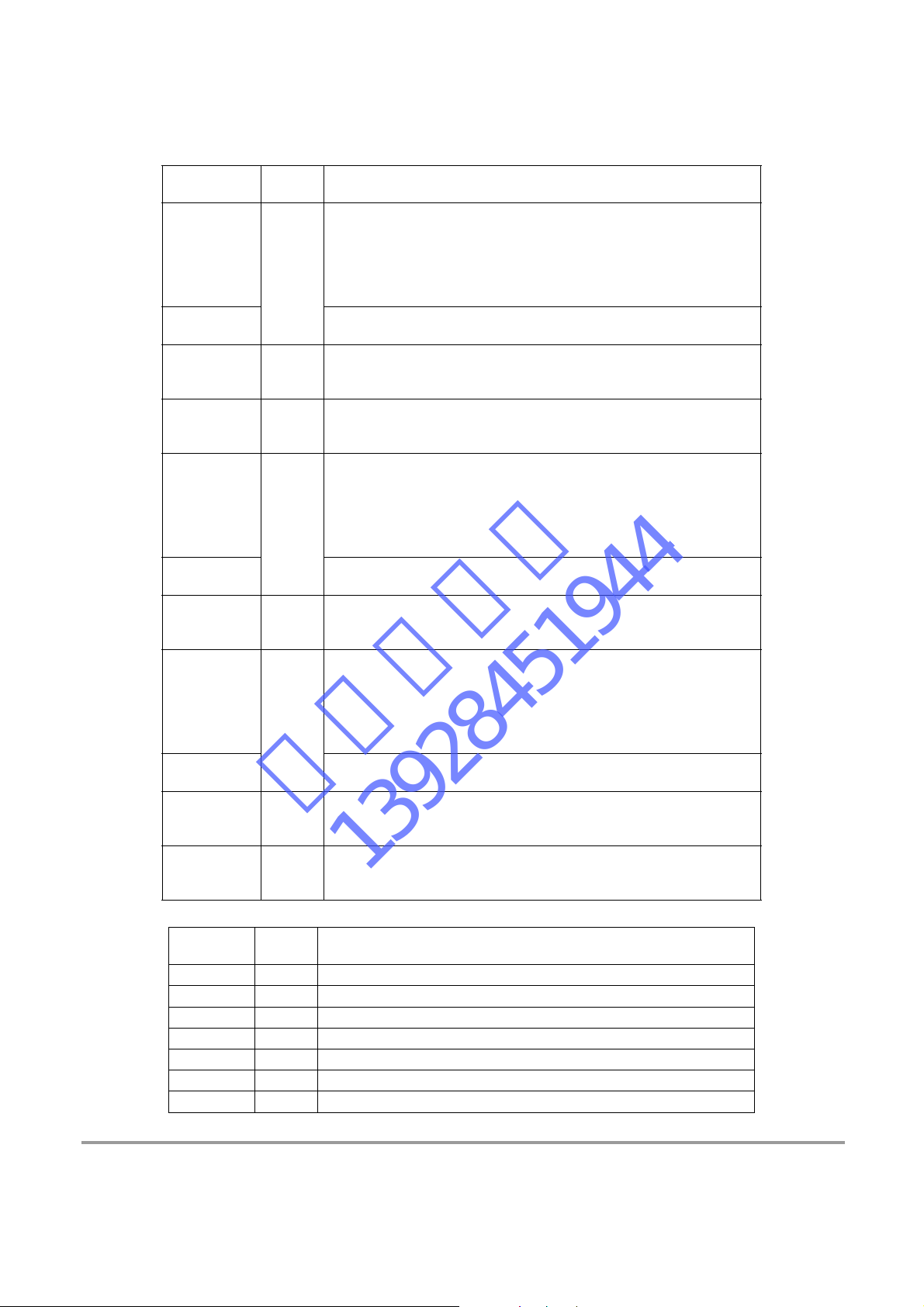
Table 2-4 Transmitter Pins
NAME
TX01-
TX01+
TX11-
TX11+
TX21-
TX21+
TXC1-
TXC1+
HTPLG1 IN
EXT_SWING01 Analog
TX02-
TX02+
TX12-
TX12+
TX22-
TX22+
TXC2-
TXC2+
HTPLG2 IN
TX03-
TX03+
TX13-
TX13+
TX23-
TX23+
TXC3-
TXC3+
HTPLG3 IN
EXT_SWING23 Analog
IN /
OUT
Analog
Analog
Analog
DESCRIPTION
Differential Data Output Pairs for transmitter port 1
Differential Clock Output Pairs for transmitter port 1
Hot Plug Input
This pin is used to monitor the "HOT PLUG" signal for tansmitter port 1. Note:
This input is only 3.3V tolerant and has no internal debouncer circuit.
Voltage Swing Adjust for Port 0/1. A resistor should tie this pin to AVCC. This
resistance determines the amplitude of the voltage swing. 560: is
recommended.
Differential Data Output Pairs for transmitter port 2
Differential Clock Output Pairs for transmitter port 2
Hot Plug Input
This pin is used to monitor the "HOT PLUG" signal for tansmitter port 2. Note:
This input is only 3.3V tolerant and has no internal debouncer circuit.
Differential Data Output Pairs for transmitter port 3
Differential Clock Output Pairs for transmitter port 3
Hot Plug Input
This pin is used to monitor the "HOT PLUG" signal for tansmitter port 3. Note:
This input is only 3.3V tolerant and has no internal debouncer circuit.
Voltage Swing Adjust for Port 2/3. A resistor should tie this pin to AVCC. This
resistance determines the amplitude of the voltage swing. 560: is
recommended.
Table 2-5 Power and Ground Pins
NAME
VDDE PWR Digital Power, 3.3V
VSSE GND Digital Ground
VDD18 PWR Core Power, 1.8V
VSS GND Core Ground
AVDD PWR Analog Power, 3.3V
AVSS GND Analog Ground
PVDD PWR Analog Power for PLL, 3.3V
8
IN /
OUT
DESCRIPTION
Explore Confidential Proprietary
NON-DISCLOSURE AGREEMENT REQUIRED
Page 9
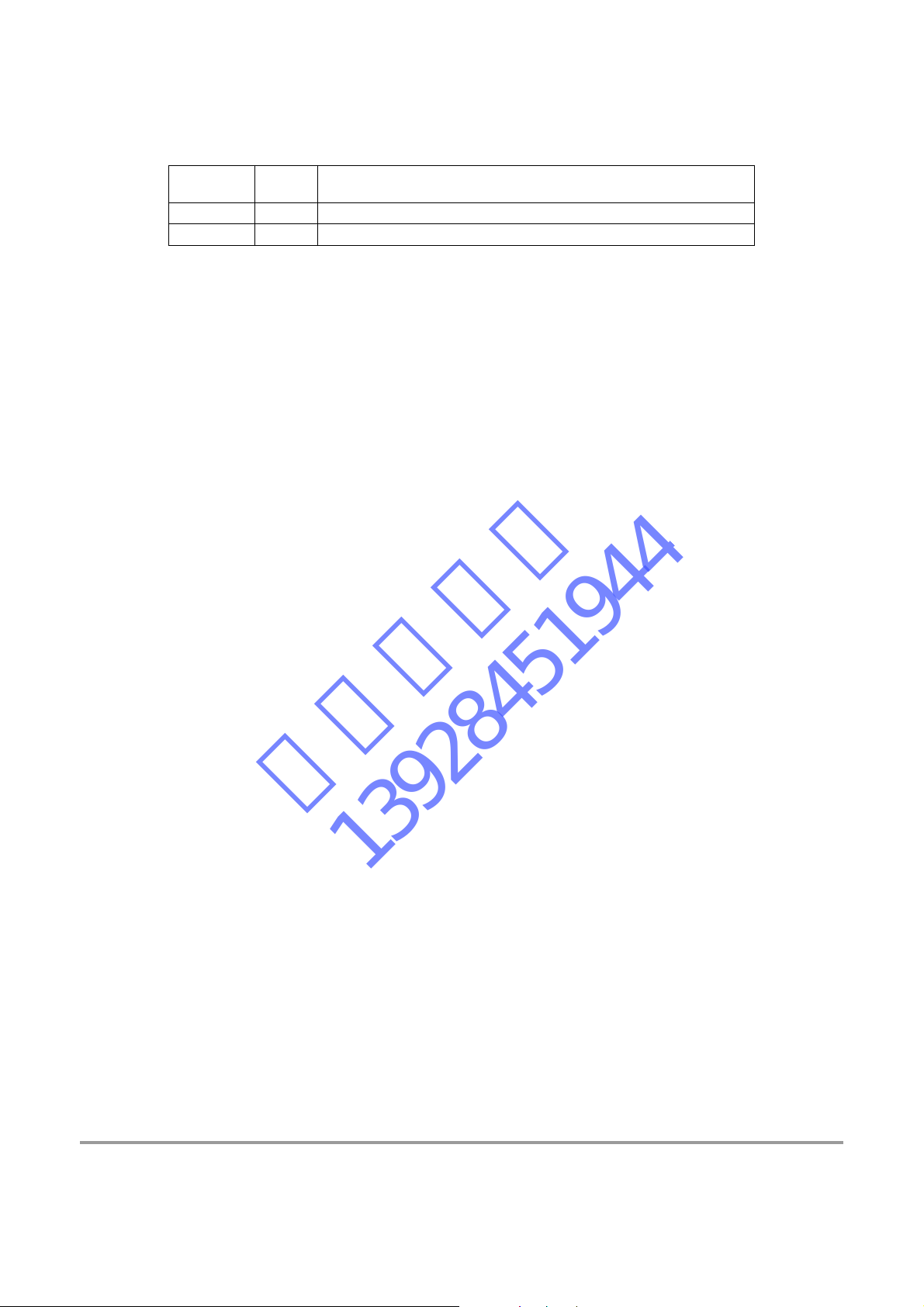
Table 2-5 Power and Ground Pins
深圳诗普睿
13928451944
User Guide — EP9134_UG V0.2
NAME
PVSS GND Analog Ground for PLL
_AVSS GND Analog Ground
IN /
OUT
DESCRIPTION
Explore Confidential Proprietary
NON-DISCLOSURE AGREEMENT REQUIRED
9
Page 10
User Guide — EP9134_UG V0.2
深圳诗普睿
13928451944
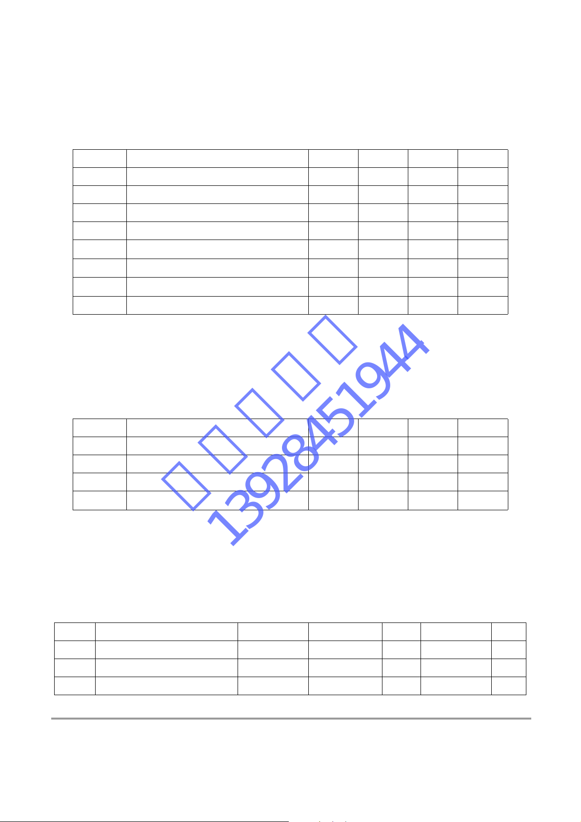
2.4 Electrical Characteristics
Absolute Maximum Conditions
Symbol Parameter Min Typ Max Units
Vcc33 3.3V Supply Voltage -0.3 4.0 V
Vcc18 1.8V Supply Voltage -0.3 2.5 V
V
I
V
O
T
A
T
STG
T
JA
P
PD
1 Permanent device damage may occur if absolute maximum conditions are exceeded.
2 Functional operation should be restricted to the conditions described under Normal Operating Conditions.
Ambient Temperature (with power applied) -25 75
Storage Temperature -40 125
Thermal Resistance (Junction to Ambient) 29.1
Package Power Dissipation 2.4 W
Normal Operating Conditions
Input Voltage -0.3 V
Output Voltage -0.3 V
+ 0.3 V
cc
+ 0.3 V
cc
qC
qC
qC/W
Symbol Parameter Min Typ Max Units
Vcc33 3.3V Supply Voltage 3.14 3.3 3.6 V
Vcc18 1.8V Supply Voltage 1.71 1.8 1.98 V
V
CCN
T
A
1 Guaranteed by design.
Ambient Temperature (with power applied) 0 25 70
Supply Voltage Noise
1
-0.3 100 mV
p-p
qC
DC Digital I/O Specifications (under normal operating conditions unless otherwise specified)
Symbol Parameter Conditions Min Typ Max Units
V
IH
V
IL
V
OH
High-level Input Voltage 2.0 V
Low-level Input Voltage 0.8 V
High-level Output Voltage 2.4 V
10
Explore Confidential Proprietary
NON-DISCLOSURE AGREEMENT REQUIRED
Page 11
User Guide — EP9134_UG V0.2
深圳诗普睿
13928451944
V
OL
I
OL
V
ID
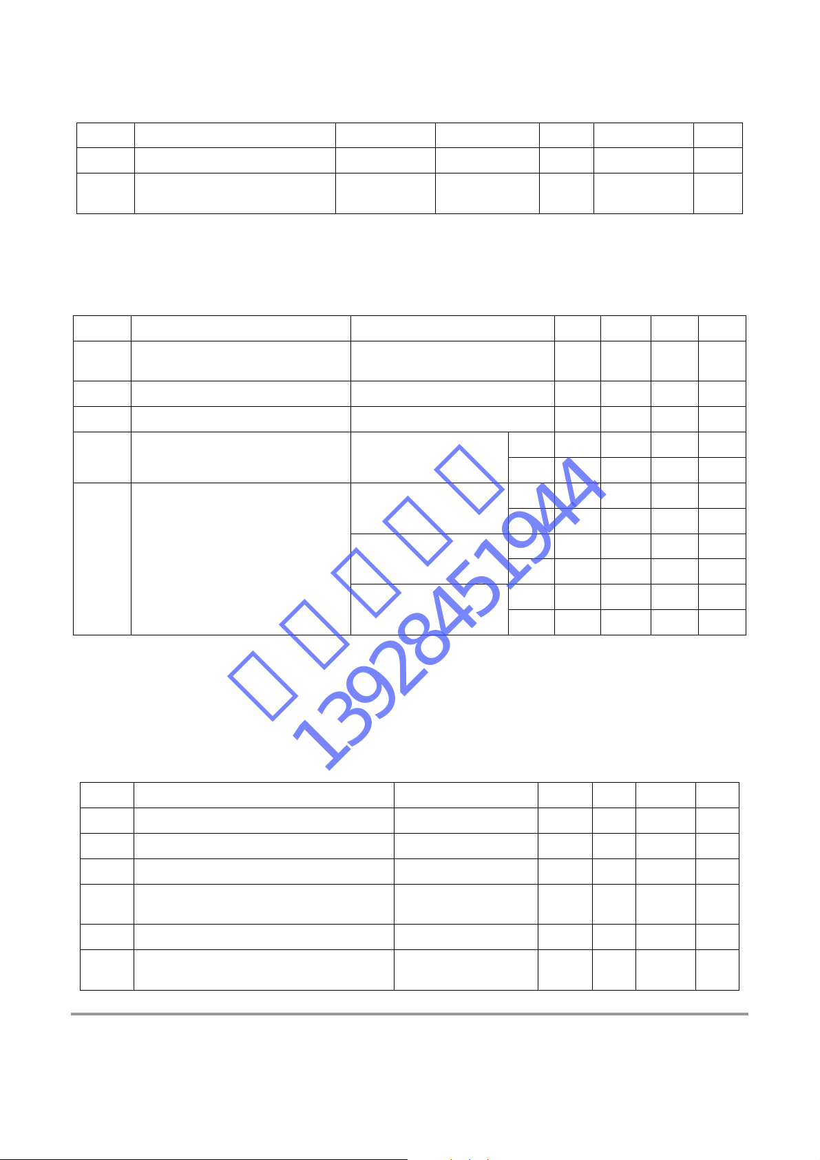
DC Analogue Specifications (under normal operating conditions unless otherwise specified)
Symbol Parameter Conditions Min Typ Max Units
V
OD
V
DOH
I
DOS
I
PD
I
CCD
Low-level Output Voltage 0.4 V
Output Leakage Current High Impedance -10 10 uA
Differential Input Voltage, Single
Ended Amplitude
Differential Voltage
Single ended peak to peak amplitude
Differential High-level Output Voltage
Differential Output Short Circuit Current V
Power-Down Current
Supply Current
(25qC Ambient,
R
EXT_SWING
= 430 ohm,
2
1
1080p Resolution (8-bit)
UXGA Resolution (8-bit)
R
LOAD
R
EXT_SWING
25qC Ambient
TX0/TX1/TX2/TX3 are Active)
1080p Resolution (12-bit)
OUT
150 1000 mV
= 50 ohm
= 430 ohm
= 0V 5 V
3V3 2 mA
1V8 1 mA
3V3 440 mA
1V8 110 mA
3V3 449 mA
1V8 110 mA
3V3 484 mA
1V8 164 mA
510 550 590 mV
AVCC mV
1 Guaranteed by design.
2 Assumes all HDMI/DVI I/O ports are not connected and all digital inputs are scilent.
Receiver AC Specifications (under normal operating conditions unless otherwise specified)
Symbol Parameter Conditions Min Typ Max Units
2,3
1
4
1
25 40
T
T
T
T
T
T
DPS
CCS
IJIT
PDL
HSC
FSC
Intra-Pair (+ to -) Differential Input Skew
Channel to Channel Differential Input Skew1 1.0 T
Differential Input Clock Jitter Tolerance
Delay from OUT_EN Low to High Impedance
outputs
Link Disabled (Tx power down) to LINK_ON Low
Link Enabled (DE Active) to LINK_ON High
0.4 T
0.3 T
10 ns
250 ms
Explore Confidential Proprietary
NON-DISCLOSURE AGREEMENT REQUIRED
bit
pixel
bit
DE
edges
11
 Loading...