


ESI
ESI
Excel Semiconductor inc.
ES29LV320D
32Mbit(4M x 8/2M x 16)
CMOS 3.0 Volt-only, Boot Sector Flash Memory
GENERAL FEATURES
• Single power supply operation
- 2.7V -3.6V for read, program and erase operations
•Sector Structure
- 8Kbyte x 8 boot sectors
- 64Kbyte x 63 sectors
- 256byte security sector
• Top or Bottom boot block
- ES29LV320DT for Top boot block device
- ES29LV320DB for Bottom boot block device
• A 256 bytes of extra sector for security code
- Factory lockable
- Customer lockable
• Package Options
- 48-pin TSOP
- Pb-free packages
- All Pb-free products are RoHS-Compliant
• Low Vcc write inhibit
• Manufactured on 0.18um process technology
• Compatible with JEDEC standards
- Pinout and software compatible with single-power
supply flash standard
DEVICE PERFORMANCE
• Read access time
- 90ns/120n for normal Vcc range ( 2.7V - 3.6V )
- 80ns for regulated Vcc range ( 3.0V - 3.6V )
• Program and erase time
- Program time : 9us/byte, 11us/word ( typical )
- Accelerated program time : 8us/word ( typical )
- Sector erase time : 0.7sec/sector ( typical )
• Power consumption (typical values)
- 200nA in standby or automatic sleep mode
- 10 mA active read current at 5 MHz
- 15mA active write current during program or erase
• Minimum 100,000 program/erase cycles per sector
• 20 Year data retention at 125
o
C
SOFTWARE FEATURES
• Erase Suspend / Erase Resume
• Data# poll and toggle for Pro gr a m/erase status
• CFI ( Common Flash Interface) supported
• Unlock Bypass program
• Autoselect mode
• Auto-sleep mode after t
ACC
+ 30ns
HARDWARE FEATURES
• Hardware reset input pin ( RESET#)
- Provides a hardware reset to device
- Any internal device operation is terminated and the
device returns to read mode by the reset
• Ready/Busy# output pin ( RY/BY#)
- Provides a program or erase operational status
about whether it is finished for read or still being
progressed
• WP#/ACC input pin
- Two outermost boot sectors are protected when
WP# is set to low, regardless of sector protection
- Program speed is accelerated by raising WP#/ACC
to a high voltage (12V)
• Sector protection / unprotection ( RESET# , A9 )
- Hardware method of locking a sector to prevent
any program or erase operation within that sector
- Two methods are provided :
- In-system method by RESET# pin
- A9 high-voltage method for PROM programmers
• Temporary Sector Unprotection ( RESET# )
- Allows temporary unprotection of previously
protected sectors to change data in-system
ES29LV320D
1
Rev. 2D Jan 5, 2006

GENERAL PRODUCT DESCRIPTION
ESI
ESI
Excel Semiconductor inc.
The ES29LV320 is a 32 megabit, 3.0 volt-only flash
memory device, organized as 4M x 8 bits (Byte
mode) or 2M x 16 bits (Word mode) which is configurable by BYTE#. Eight boot sectors and sixty three
main sectors with uniform size are provided :
8Kbytes x 8 and 64Kbytes x 63. The device is manufactured with ESI’s proprietary, high performance
and highly reliable 0.18um CMOS flash technology.
The device can be programmed or erased in-system with standard 3.0 Volt Vcc supply ( 2.7V-3.6V)
and can also be programmed in standard EPROM
programmers. The device offers minimum e ndurance of 100,000 program/erase cycles and more
than 10 years of data retention.
The ES29LV320 offers access time as fast as 80ns
or 90ns, allowing operation of high-speed microprocessors without wait states. Three separate control
pins are provided to eliminate bus contention : chip
enable (CE#), write enable (WE#) and output
enable (OE#).
All program and erase operation are automatically
and internally performed and controlled by embedded program/erase algorithms built in the device.
The device automatically generates and times the
necessary high-voltage pulses to be applied to the
cells, performs the verification, and counts the number of sequences. Some status bits (DQ7, DQ6 and
DQ5) read by data# polling or toggling between
consecutive read cycles provide to the users the
internal status of program/erase operation: whether
it is successfully done or still being progressed.
Extra Security Sector of 256 bytes
In the device, an extra security sector of 256 bytes is
provided to customers. This extra sector can be
used for various purposes such as storing ESN
(Electronic Serial Number) or customer’s security
codes. Once after the extra sector is written, it can
be permanently locked by the device manufacturer(
factory-locked) or a customer( customer-lockable). At the same time, a lock indicator bit (DQ7)
is permanently set to a 1 if the part is factory- locked,
or set to 0 if it is customer-lockable. Therefore, this
lock indicator bit (DQ7) can be properly used to
avoid that any customer-lockable part is used to
replace a factory-locked part. The extra security
sector is an extra memory space for customers
when it is used as a customer-lockable version. So,
it can be read and written like any other sectors. But
it should be noted that the number of E/W(Erase and
Write) cycles is limited to 300 times (maximum) only
in the Security Sector.
Special services such as ESN and factory-lock are
available to customers ( ESI’s Special-Code ser-
vice ) The ES29L V320 is completely comp atible with
the JEDEC standard command set of single power
supply Flash. Commands are written to the internal
command register using standard write timings of
microprocessor and data can be re ad out from the
cell array in the device with the same way as used i n
other EPROM or flash devices.
ES29LV320D
2
Rev. 2D Jan 5, 2006
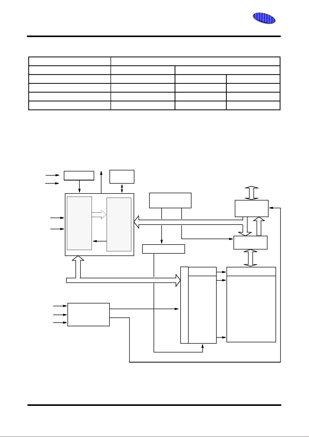
PRODUCT SELECTOR GUIDE
Family Part Number ES29LV320
Voltage Range 3.0 ~ 3.6V 2.7 ~ 3.6V
Speed Option 80R 90 120
Max Access Time (ns) 80 90 120
CE# Access (ns) 80 90 120
OE# Access (ns) 35 40 50
FUNCTION BLOCK DIAGRAM
RY/BY#
ESI
ESI
Excel Semiconductor inc.
Vcc
Vss
WE
RESET#
A<0:20
CE#
OE#
BYTE#
Vcc Detector
#
Command
Register
Timer/
Counter
Write
State
Machine
Analog Bias
Generator
Sector Switches
Y-Decoder
DQ0-DQ15(A-1)
Input/Output
Buffers
Data Latch/
Sense Amps
Y-Decoder
>
Cell Array
Chip Enable
Output Enable
Logic
X-Decoder
Address Latch
ES29LV320D
3
Rev. 2D Jan 5, 2006
PIN DESCRIPTION
Pin Description
A0-A20 21 Addresses
DQ0-DQ14 15 Data Inputs/Outputs
DQ15/A-1
CE# Chip Enable
OE# Output Enable
WE# Write Enable
WP#/ACC Hardware Write Protect/Acceleration Pin
RESET# Hardware Reset Pin, Active Low
BYTE# Se lects 8-bit or 16-bit mode
RY/BY# Ready/Busy Output
Vcc
Vss Device Ground
NC Pin Not Connected Internally
Excel Semiconductor inc.
DQ15 (Data Input/Output, Word Mode)
A-1 (LSB Address Input, Byte Mode)
3.0 volt-only single power supply
(see Product Selector Guide for speed options and voltage supply tolerances)
ESI
ESI
LOGIC SYMBOL
21
A0 ~ A20
CE#
OE#
WE#
WP#/ACC
RESET#
BYTE#
16 or 8
DQ0 ~ DQ15
(A-1)
RY/BY#
ES29LV320D
4
Rev. 2D Jan 5, 2006

CONNECTION DIAGRAM
ESI
ESI
Excel Semiconductor inc.
A15
A14
A13
A12
A11
A10
A9
A8
A19
A20
WE#
RESET#
NC
WP#/ACC
RY/BY#
A18
A17
A7
A6
A5
A4
A3
A2
A1
1
2
3
4
5
6
7
8
9
10
11
12
13
14
15
16
17
18
19
20
21
22
23
24
48-Pin Standard TSOP
ES29LV320
48
47
46
45
44
43
42
41
40
39
38
37
36
35
34
33
32
31
30
29
28
27
26
25
A16
BYTE#
Vss
DQ15/A-1
DQ7
DQ14
DQ6
DQ13
DQ5
DQ12
DQ4
Vcc
DQ11
DQ3
DQ10
DQ2
DQ9
DQ1
DQ8
DQ0
OE#
Vss
CE#
A0
ES29LV320D
5
Rev. 2D Jan 5, 2006

DEVICE BUS OPERATIONS
ESI
ESI
Excel Semiconductor inc.
Several device operational modes are provided in
the ES29LV320 device. Commands are used to initiate the device operations. They are latched and
stored into internal registers with the address and
data information needed to execute the device
operation.
The available device operational modes are listed
in Table 1 with the required inputs, controls, and the
resulting outputs. Each operational mode is
described in further detail in the following subsections.
Read
The internal state of the device is set for the read
mode and the device is ready for reading arra y da t a
upon device power-up, or after a hardware reset. To
read the stored data from the cell array of the
device, CE# and OE# pins should be driven to V
while WE# pin remains at VIH. CE# is the power
control and selects the device. OE# is the output
control and gates array data to the output pins.
Word or byte mode of output data is determined by
the BYTE# pin. No additional command is needed
in this mode to obtain array data. Standard microprocessor read cycles that assert valid addresses
on the device address inputs produce valid data on
the device data outputs. The device st ays at the read
mode until another operation is activated by writing
commands into the internal command register. Refer
to the AC read cycle timing diagrams for further
details ( Fig. 18 ).
Word/Byte Mode Configuration ( BYTE# )
The device data output can be configured by BYTE#
into one of two modes : word and byte modes. If the
BYTE# pin is set at logic ‘1’, the device is configured
in word mode, DQ0 - DQ15 are active and controlled
by CE# and OE#. If the BYTE# pin is set at logic ‘0’,
the device is configured in byte mode, and only data
I/O pins DQ0 - DQ7 are active and controlled by CE#
and OE#. The data I/O pins DQ8 - DQ14 are tristated, and the DQ15 pin is used as an input for the
LSB (A-1) address.
IL
Standby Mode
When the device is not selected or activated in a
system, it needs to stay at the standby mode, in
which current consumption is greatly reduced with
outputs in the high impedance state.
ES29LV320D
6
Rev. 2D Jan 5, 2006

ESI
ESI
Excel Semiconductor inc.
The device enters the CMOS standby mode when
CE# and RESET# pins are both held at Vcc
+
0.3V.
(Note that this is a more restricted voltage range
than V
not within Vcc
) If CE# and RESET# are held at VIH, but
IH.
+
0.3V, the device will be still in the
standby mode, but the standby current will be
greater than the CMOS standby current (0.2uA typically). When the device is in the standby mode, only
standard access time (t
) is required for read
CE
access, before it is ready for read data. And even if
the device is deselected by CE# pin during erase or
programming operation, the device draws active cur rent until the operation is completely done. While the
device stays in the standby mode, the output is
placed in the high impedance state, independent of
the OE# input.
The device can enter the deep power-down mode
where current consumption is greatly reduced down
to less than 0.2uA typically by the following three
ways:
- CMOS standby ( CE#, RESET# = Vcc + 0.3V )
- During the device reset ( RESET# = Vss
- In Autosleep Mode ( after t
ACC
+ 30ns )
+ 0.3V )
Refer to the CMOS DC characteristics Table11 for
further current specification .
Autosleep Mode
The device automatically enters a deep power-down
mode called the autosleep mode when addresses
remain stable for t
consumption is greatly reduced ( less than 0.2uA
typical ), regardless of CE#, WE# and OE# control
signals.
+30ns. In this mode, current
ACC
set-up cycle and the last cycle with the program
data and addresses. In this mode, two unlock
cycles are saved ( or bypassed ).
Sector Addresses
The entire memory space of cell array is divided
into a many of small sectors: 8kbytes x 8 boot sectors and 64Kbytes x 63 main sectors. In erase
operation, a single sector, multiple sectors, or the
entire device (chip erase) can be selected for
erase. The address space that each sector occupies is shown in detail in the Table 3-4.
Accelerated Program Mode
The device offers accelerated program operations
through the ACC function. This is one of two functions provided by the WP#/ACC pin. This function
is primarily intended to allow faster manufacturing
throughput at the factory. If the system asserts V
(11.5~12.5V) on this pin, the device automatically
enters the previously mentioned Unlock Bypass
mode, temporarily unprotects any protected sectors, and uses the higher voltage on the pin to
reduce the time required for program operations.
Only two-cycle program command sequences are
required because the unlock bypass mode is automatically activated in this acceleration mode. The
device returns to the normal operation when V
removed from the WP#/ACC pin. It should be
noted that the WP#/ACC pin must not be at V
operations other than accelerated programming, or
device damage may result. In addition, the WP#/
ACC pin must not be left floating or unconnected;
inconsistent or undesired behavior of the device
may result.
HH
HH
HH
for
is
Writing Commands
To write a command or command sequences to initiate some operations such as program or erase, the
system must drive WE# and CE# to V
. For program operations, the BYTE# pin deter-
V
IH
, and OE# to
IL
mines whether the device accepts pro gram data in
bytes or words. Refer to “BYTE# timings for Write
Operations” in the Fig. 21 for more information.
Unlock Bypass Mode
To reduce more the programming time, an unlockbypass mode is provided. Once the device enters
this mode, only two write cycles are required to initiate the programming operation instead of four
cycles in the normal program command sequences
which are composed of two unlock cycles, program
ES29LV320D
7
Autoselect Mode
Flash memories are intended for use in applications where the local CPU alter s me mory cont ents.
In such applications, manufacturer and device
identification (ID) codes must be accessible while
the device resides in the target system ( the so
called “in-system program”). On the other hand,
signature codes have been typically accessed by
raising A9 pin to a high voltage in PROM programmers. However, multiplexing high voltage onto
address lines is not the generally desired system
design practice. Therefore, in the ES29LV320
device an autoselect command is provided to
allow the system to access the signature codes
without any high voltage. The conventional A9
high-voltage method used in the PROM progra mers for signature codes are still supported in this
device.
Rev. 2D Jan 5, 2006

ESI
ESI
Excel Semiconductor inc.
If the system writes the autoselect command
sequence, the device enters the Autoselect mode.
The system can then read some useful codes such
as manufacturer and device ID from the internal registers on DQ7 - DQ0. Standard read cycle timings
apply in this mode. In the Autoselect mode, the following four informations can be accessed through
either autoselect command method or A9 high-voltage autoselect method. Refer to the Table 2.
-
-
-
-
Manufacturer ID
Device ID
Security Sector Lock-indicator
Sector protection verify
Hardware Device Reset ( RESET# )
The RESET# pin provides a hardware method of
resetting the device to read array data. When the
RESET# pin is driven low for at least a period of t
the device immediately terminates any operation in
progress, tristates all output pins, and ignores all
read/write commands for the duration of the
RESET# pulse The device also resets the internal
state machine to reading array data. The operation
that was interrupted should be reinitiated once after
the device is ready to accept another command
sequence, to ensure data integrity.
RP
CMOS Standby during Device Reset
Flash memory, enabling the system to read the
boot-up firmware from the Flash memory.Refer to
the AC Characteristics tables for RESET# parameters and to Fig. 19 for the timing diagram.
SECTOR GROUP PROTECTION
The ES29LV320 features hardware sector group
protection. A sector group consists of two or more
adjacent sectors that are protected or unprotected
at the same time. In the device, sector protection is
performed on the group of sectors previously
defined in the Table 3-4. Once after a group of sectors are protected, any program or erase operation
is not allowed in the protected sector group. The
previously protected sectors must be unprotected
by one of the unprotect methods provided here
before changing data in those sectors. Sector protection can be implemented via two methods.
,
-
-
To check whether the sector group protection was
successfully executed or not, another operation
called “protect verification” needs to be performed after the protection oper ation on a group of
sectors. All protection and protect verifications provided in the device are summarized in detail at the
Table 1.
In-system protection
A9 High-voltage protection
Current is reduced for the duration of the RESET#
pulse. When RESET# is held at Vss
device draws the greatly reduced CMOS standby
current ( I
within Vss
). If RESET# is held at VIL but not
CC4
+
0.3V, the standby current will be greater.
+
0.3V, the
RY/BY# and Terminating Operations
If RESET# is asserted during a program or erase
operation, the RY/BY# pin remains a “0” (busy) until
the internal reset operation is completed, which
requires a time of t
rithms). The system can thus monitor RY/BY# to
determine whether the reset operation is completed.
If RESET# is asserted when a program or erase
operation is not executing (RY/BY# pin is “1”), the
reset operation is completed within a time of t
(not during Embedded Algorithms). The system can
read data after the RESET# pin returns to V
requires a time of t
READY
RH.
(during Embedded Algo-
READY
, which
IH
RESET# tied to the System Reset
The RESET# pin may be tied to the system reset circuitry. A system reset would thus also reset the
In-System Protection
“In-system protection”, the primary method,
requires V
A6=0, A1=1, and A0=0. This method can be implemented either in-system or via programming equipment. This method uses standard microprocessor
bus cycle timing. Refer to Fig. 29 for timing diagram
and Fig. 3 for the protection algorithm.
(11.5V~12.5V) on the RESET# with
ID
A9 High-Voltage Protection
“High-voltage protection”, the alternate method
intended only for programming equipment, must
force V
trol pin OE# with A6=0, A1=1 and A0=0. Refer to
Fig. 31 for timing diagram and Fig. 5 for the protection algorithm.
(11.5~12.5V) on address pin A9 and con-
ID
SECTOR UNPROTECTION
The previously protected sectors must be unprotected before modifying any data in the sectors.
The sector unprotection algorithm unprotects all
sectors in parallel. All unprotected sectors must first
ES29LV320D
8
Rev. 2D Jan 5, 2006
ESI
ESI
Excel Semiconductor inc.
be protected prior to the first sector unprotection
write cycle to avoid any over-erase due to the intrinsic erase characteristics of the protection cell. After
the unprotection operation, all previously protected
sectors will need to be individually re-protected.
Standard microprocessor bus cycle timings are used
in the unprotection and unprotect verification operations. Three unprotect methods are provided in the
ES29LV320 device. All unprotection and unprotect
verification cycles are summarized in detail at the
Table 1.
-
-
-
In-system unprotection
A9 High-voltage unprotection
T emporary sector unprotection
In-System Unprotection
“In-system unprotection”, the primary method,
requires V
A6=1, A1=1, and A0=0. This method can be implemented either in-system or via programming equipment. This method uses standard microprocessor
bus cycle timing. Refer to Fig. 29 for timing diagram
and Fig. 4 for the unprotection algorithm.
(11.5V~12.5V) on the RESET# with
ID
If the system asserts V
on the WP#/ACC pin, the
IL
device disables program and erase func tions in the
two “outermost” 8Kbytes boo t sectors independently of whether those sectors were protected or
unprotected using the method described in “Sector
Group Protection and Unprotection”. The two outermost of 8 Kbyte boot sectors are the two sectors
containing the lowest addresses in a bottom-bootconfigured device, or the two sectors containing the
highest addresses in a top-boot-configured device.
If the system asserts V
on the WP#/ACC pin, the
IH
device reverts to whether the two outermost 8
Kbyte boot sectors were last set to be protected or
unprotected. That is, sector protection or unprotection for these two sectors depends on whether they
were last protected or unprotected using the
method described in “Sector Group Protection and
Unprotection”.
Note that the WP#/ACC pin must not be left floating
or unconnected; inconsistent behavior of the device
may result.
A9 High-Voltage Unprotection
“High-voltage unprotection”, the alternate method
intended only for programming equipment, must
force V
(11.5~12.5V) on address pin A9 and con-
ID
trol pin OE# with A6=1, A1=1 and A0=0. Refer to
Fig. 32 for timing diagram and Fig. 6 for the unprotection algorithm.
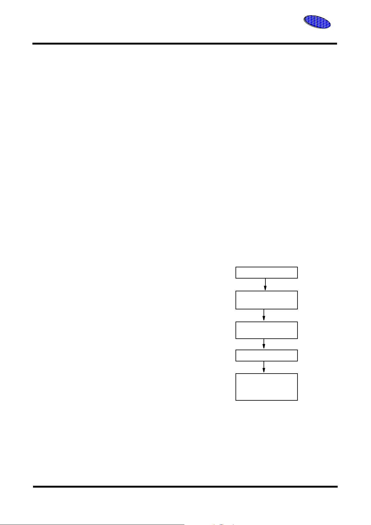
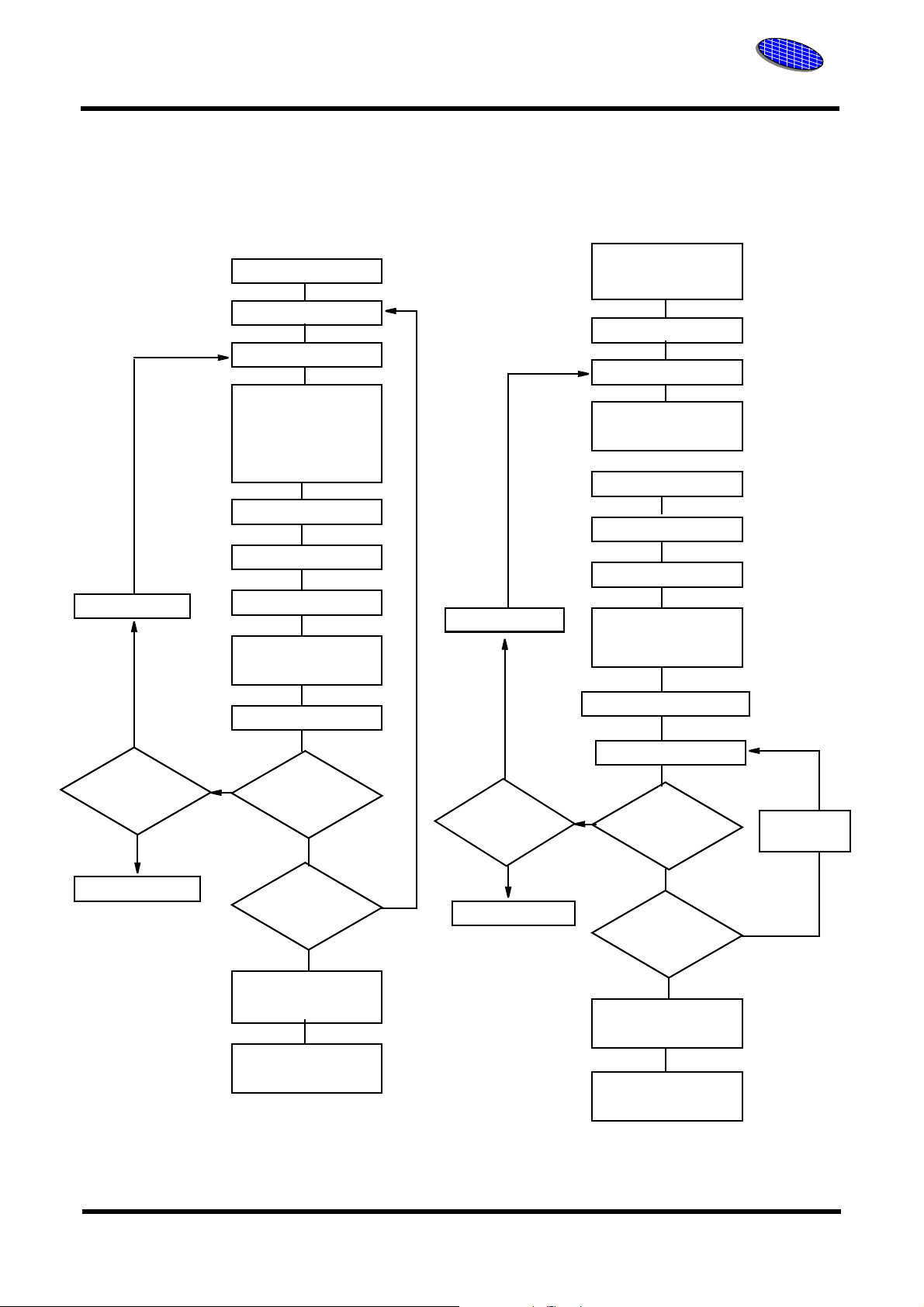
Temporary Sector Unprotect
This feature allows temporary unprotection of previously protected sectors to change data in-system.
The Sector Unprotect mode is activated by setting
the RESET# pin to V
(11.5V-12.5V). During this
ID
mode, formerly protected sectors can be programmed or erased by selecting the sector
addresses. Once V
is removed from the RESET#
ID
pin, all the previously protected sectors are protected again. Fig. 1 shows the algorithm, and Fig. 27
shows the timing diagrams for this feature.
WRITE PROTECT ( WP# )
The Write Protect function provides a hardware
method of protecting certain boot sectors without
using V
WP#/ACC pin.
. This function is one of two provided by the
ID
START
RESET# = V
(Note 1)
Perform Erase or
Program Operations
RESET# = V
Temporary Sector
Unprotect Completed
(Note 2)
Notes:
1. All protected sectors are unprotected (If WP#/ACC = VIL,
outermost boot sectors will remain protected).
2. All previously protected sectors are protected once again.
ID
IH
Figure 1. Temporary Sector Unprotect
Operation
ES29LV320D
9
Rev. 2D Jan 5, 2006

SECURITY SECTOR
The security sector of the ES29LV320 device provides an extra flash memory space that enables
permanent part identification through an Electronic
Serial Number (ESN). The security sector uses a
security lock-Indicator Bit (DQ7) to indicate
whether or not the security sector is locked when
shipped from the factory. This bit is permanently set
at the factory and cannot be changed, which prevents cloning of a factory locked part. This ensures
the security of the ESN once the product is shipped
to the field. Note that the ES29LV320 has a security
sector size of 256 bytes.
Security Lock-Indicator Bit (DQ7)
In the device, the security sector can be provided in
either factory locked version or customer lockable
version. The factory-locke d version is always protected when shipped from the factory, and has the
security lock-Indicator Bit permanently set to a “1”.
The customer-lockable version is shipped with
the security sector unprotected, allowing customers
to utilize the sector in any manner they choose. The
customer-lockable version has the security lockIndicator Bit permanently set to a “0”. Thus, the
security lock-Indicator Bit prevents customer-lockable devices from being used to replace devices
that are factory locked.
ESI
ESI
Excel Semiconductor inc.
- A random, secure ESN (16 bytes ) only
- Customer code through the ESI’s Special-Code
service
- Both a random, secure ESN and customer
code through the ESI’s Special-Code service.
ESN ( Electronic Serial Number )
In devices that have an ESN, a Bottom Boot device
will have the 16-byte (8-word) ESN in sector 0 at
addresses 000000h-00000Fh in byte mode (or
000000h-000007h in word mode). In the Top Boot
device the ESN will be in sector 70 at addresses
3FFF00h-3FFF0Fh in byte mode (or 1FFF80h1FFF87h in word mode). Note that in upcoming top
boot versions of this device, the ESN will be located
in sector 70 at addresses 3FFF00h-3FFF0Fh in byte
mode (or 1FFF80h-1FFF87h in word mode).
ESI’s Special-Code Service
Customers may opt to have their code programmed
by ESI through the ESI’s Special-Code service. ESI
programs the customer’s code, with or without the
random ESN. The devices are then shipped from
ESI’s factory with the Security Sector permanently
locked. Contact an ESI representative for details on
using ESI’s Special-Code service.
Customer-Lockable Device
Access to the Security Sector
The security sector can be accessed through a
command sequence: Enter security and Exit
security sector commands. After the system has
written the Enter security sector command
sequence, it may read the security sector by using
the addresses normally occupied by the boot sectors. This mode of operation continues until the system issues the Exit security sector command
sequence, or until power is removed from the
device. On power-up, or following a hardware reset,
the device returns to read mode in which the normal boot sectors can be accessed, instead of the
security sector.
Factory-Locked Device
In a factory-locked device, the security sector is
protected when the device is shipped from the factory. The security sector cannot be mo dified in any
way. The device is available preprogrammed with
one of the following:
The customer lockable version allows the security
sector to be freely programmed or erased and then
permanently locked. Note that the ES29LV320 has
a security sector size of 256 bytes (128 words). Note
that the accelerated programming (ACC) and unlock
bypass functions are not available when programming the security sector.
Protection of the Security Sector
The security sector area can be prot ected using the
following procedures: Write the three-cycle “Enter
security sector command” sequence, and then following the in-system sector protect algorithm as
shown in Fig. 2, except that RESET# may be at
either V
of the security sector without raising any device pin
to a high voltage. Note that this method is only applicable to the security sector. To verify the protect/
unprotect status of the security sector. follow the
algorithm shown in Fig. 2.
or VID. This allows in-system protection
IH
ES29LV320D
10
Rev. 2D Jan 5, 2006

Start
RESET# =
or V
V
IH
ID
Wait 1us
Write 60h to
any address
Write 40h to security
sector address with
A6=0, A1=1,A0=0
Read from security
sector address with
A6=0,A1=1,A0=0
If data=00h, security
sector is unprotected.
If data=01h, security
sector is protected
Remove V
from RESET#
Write reset
command
Security sector
Protect Verify
complete
IH
or V
ID
ESI
ESI
Excel Semiconductor inc.
can only occur after successful completion of specific command sequences. And several features are
incorporated to prevent inadvertent write cycles
resulting from Vcc power-up and power-down transition or system noise.
Low Vcc Write inhibit
When Vcc is less than V
accept any write cycles. This protects data during
Vcc power-up and power-down. The command register and all internal program/erase circuits are disabled, and the device resets to the read mode.
Subsequent writes are ignored until Vcc is greater
than V
. The system must provide proper signals
LKO
to the control pins to prevent unintentional writes
when Vcc is greater than V
, the device does not
LKO
.
LKO
Write Pulse “Glitch” Protection
Noise pulses of less than 5ns (typical) on OE#, CE#
or WE# do not initiate a write cycle.
Figure 2. Security Sector Protect Verify
Exit from the Security Sector
Once the Security Sector is locked protected and
verified, the system must write the Exit Security
Sector Region command sequence to return to
reading and writing the remainder of the array.
Caution for the Security Sector Protection
The security sector protection must be used with
caution since, once protected, there is no procedure available for unprotecting the security sector
area and none of the bits in the security sector
memory space can be modified in any way.
HARDWARE DATA PROTECTION
The ES29LV320 device provides some protection
measures against accidental erasure or programming caused by spurious system level signals that
may exist during power transition. During powerup, all internal registers and latches in the device
are cleared and the device automatically resets to
the read mode. In addition, with its internal state
machine built-in the device, any alteration of the
memory contents or any initiation of new operation
Logical inhibit
Write cycles are inhibited by holding any one of
OE#=V
, CE#=VIH or WE#=VIH. To initiate a write
IL
cycle, CE# and WE# must be a logical zero while
OE# is a logical one.
Power-up Write Inhibit
If WE#=CE#=VIL and OE#=VIH during power up, the
device does not accept any commands on the rising
edge of WE#. The internal state machine is automatically reset to the read mode on power-up.
ES29LV320D
11
Rev. 2D Jan 5, 2006
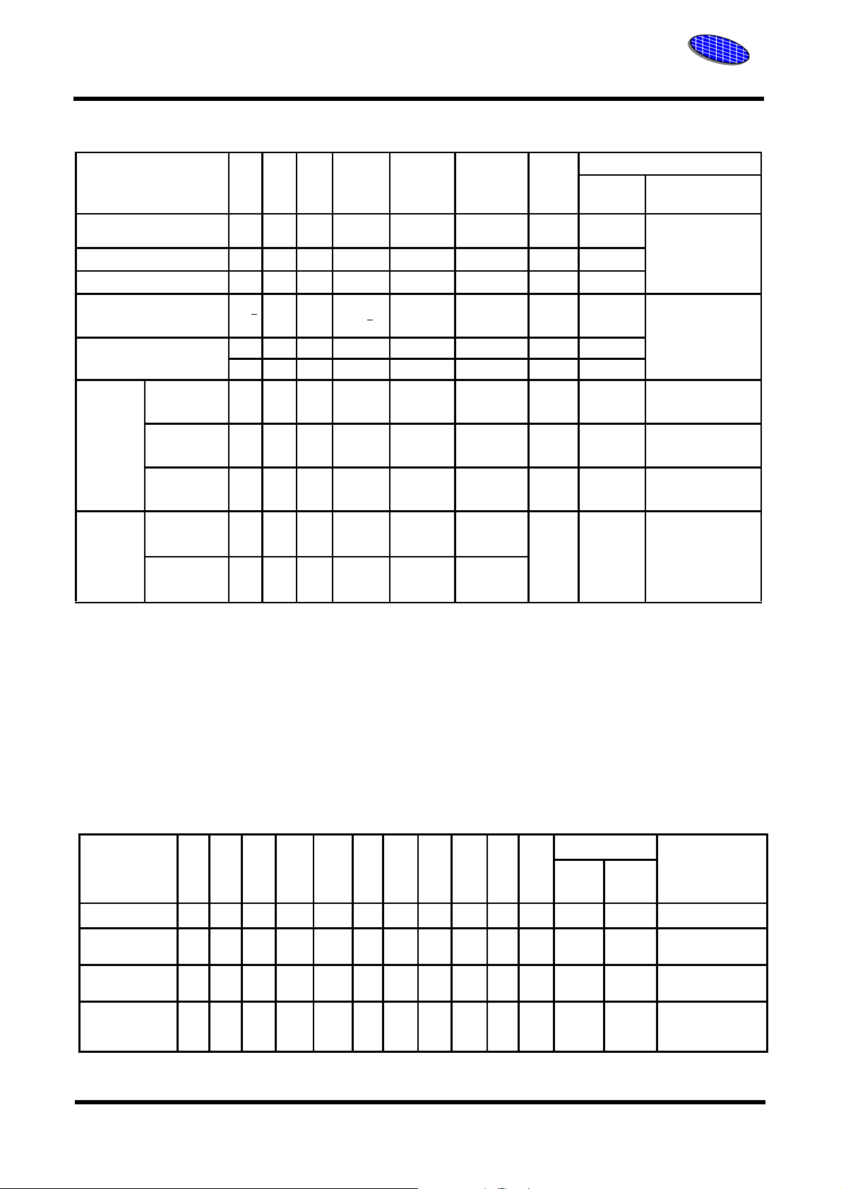
Table 1. ES29LV320 Device Bus Operations
ESI
ESI
Excel Semiconductor inc.
Operation CE# OE# WE# RESET# WP#/ACC Addresses
Read
Accelerated Program L H L H
Standby
Output Disable
Reset
Sector Protect
(Note 2)
In-system
A9 High-Voltage Method
Sector Unprotect
(Note 2) L H L V
Temporary Sector Unprotect X X X
Sector protect
Sector unprotect
L
L
Vcc+
0.3V
L H H H L/H X High-Z High-Z
X X X L L/H X High-Z High-Z
LHL
L
L
H
L
L
H
X X Vcc+
V
ID
V
ID
0.3V
L
L
HL/H
H (Note 3)
V
HH
H X High-Z High-Z
V
ID
ID
V
ID
H
H
L/H
L/H
(Note 3)
H
(Note 3)
H
(Note 3)
H
(Note 3)
(Note 1)
A
IN
A
IN
A
IN
SA,A6=L,
A1=H,A0=L
SA,A6=H,
A1=H,A0=L
A
IN
SA,A9=V
A6=L,
A1=H,A0=L
SA,A9=V
A6=H,
A1=H,A0=L
DQ0
~
DQ7
D
OUT
(Note 4) (Note 4)
(Note 4) (Note 4)
(Note 4) X X
(Note 4) X X
(Note 4) (Note 4) High-Z
,
ID
(Note 4) (Note 4) High-Z
,
ID
BYTE#
= V
D
OUT
DQ8~DQ15
IH
BYTE#
= V
IL
DQ8~DQ14 = High-Z,
DQ15 = A-1Write
High-Z
Legend:
A
L=Logic Low=VIL, H=Logic High=VIH, VID=11.5-12.5V, VHH=11.5-12.5V, X=Don’t Care, SA=Sector Address,
=Address In, DIN=Data In, D
IN
=Data Out
OUT
Notes:
1. Addresses are A20:A0 in word mode (BYTE#=VIH) , A20:A-1 in byte mode (BYTE#=VIL).
2. The sector protect and sector unprotect funct ions may als o be implement ed via programming eq uipment. See the “Sector/ Sector
Block Protection and Unprotection” section.
3. If WP#/ACC=V
, the two outermost boot sectors remain protected. If WP#/ACC=VIH, the two outermost boot sector protection
IL
depends on whether they were last protected or unprotected using the method described in “Sector/Sector Block Protection and
Unprotection”. If WP#/ACC=V
4. D
IN
or D
as required by command sequence, data polling, or sector protection algorithm.
OUT
, all sectors will be unprotected.
HH
Table 2. Autoselect Codes (A9 High-Voltage Method)
A20
Description CE# OE# WE#
to
A12
ManufactureID:ESI
Device ID:
ES29LV320
Sector Protection
Verification
Security Sector
Indicator Bit(DQ7) L L H X X
L
LLHX X
LLHSAX
H
L
XX
A11
to
A10
A9A8toA7A6
V
XLXLL X
ID
V
X L X L H 22h X F6(T),F9h(B)
ID
V
XLXHL X X
ID
V
XLXHH X X
ID
A5
toA2A1 A0
DQ8~DQ15
BYTE#
= V
IH
BYTE#
= V
IL
X4Ah
DQ7~DQ0
01h(protected)
00h(unprotected)
99h(factory-locked),
19h(customer-lock-
able)
Legend:
T= Top Boot Block, B = Bottom Boot Block, L=Logic Low=VIL, H=Logic High=VIH, SA=Sector Address, X = Don’t care
ES29LV320D
12
Rev. 2D Jan 5, 2006
Table 3. Top Boot Sector Addresses (ES29LV320DT)
ESI
ESI
Excel Semiconductor inc.
Group Sector
SA0 000000XXX 64/32 000000h~00FFFFh 000000h~07FFFh
SG0
SG1
SG2
SG3
SG4
SG5
SG6
SG7
SG8
SG9
SG10
SG11
SG12
SG13
SA1 000001XXX 64/32 010000h~01FFFFh 008000h~0FFFFh
SA2 000010XXX 64/32 020000h~02FFFFh 010000h~17FFFh
SA3 000011XXX 64/32 030000h~03FFFFh 018000h~01FFFFh
SA4 000100XXX 64/32 040000h~04FFFFh 020000h~027FFFh
SA5 000101XXX 64/32 050000h~05FFFFh 028000h~02FFFFh
SA6 000110XXX 64/32 060000h~06FFFFh 030000h~037FFFh
SA7 000111XXX 64/32 070000h~07FFFFh 038000h~03FFFFh
SA8 001000XXX 64/32 080000h~08FFFFh 040000h~047FFFh
SA9 001001XXX 64/32 090000h~09FFFFh 048000h~04FFFFh
SA10 001010XXX 64/32 0A0000h~0AFFFFh 050000h~057FFFh
SA11 001011XXX 64/32 0B0000h~0BFFFFh 058000h~05FFFFh
SA12 001100XXX 64/32 0C0000h~0CFFFFh 060000h~067FFFh
SA13 001101XXX 64/32 0D0000h~0DFFFFh 068000h~06FFFFh
SA14 001110XXX 64/32 0E0000h~0EFFFFh 070000h~077FFFh
SA15 001111XXX 64/32 0F0000h~0FFFFFh 078000h~07FFFFh
SA16 010000XXX 64/32 100000h~10FFFFh 080000h~087FFFh
SA17 010001XXX 64/32 110000h~11FFFFh 088000h~08FFFFh
SA18 010010XXX 64/32 120000h~12FFFFh 090000h~097FFFh
SA19 010011XXX 64/32 130000h~13FFFFh 098000h~09FFFFh
SA20 010100XXX 64/32 140000h~14FFFFh 0A0000h~0A7FFF h
SA21 010101XXX 64/32 150000h~15FFFFh 0A8000h~0AFFFFh
SA22 010110XXX 64/32 160000h~16FFFFh 0B0000h~0B7FFF h
SA23 010111XXX 64/32 170000h~17FFFFh 0B8000h~0BFFFFh
SA24 011000XXX 64/32 180000h~18FFFFh 0C0000h~0C7FFFh
SA25 011001XXX 64/32 190000h~19FFFFh 0C8000h~0CFFFFh
SA26 011010XXX 64/32 1A0000h~1AFFFFh 0D0000h~0D7FFFh
SA27 011011XXX 64/32 1B0000h~1BFFFFh 0D8000h~0DFFFFh
SA28 011100XXX 64/32 1C0000h~1CFFFFh 0E0000h~0E7FFFh
SA29 011101XXX 64/32 1D0000h~1DFFFFh 0E8000h~0EFFFFh
SA30 011110XXX 64/32 1E0000h~1EFFFFh 0F0000h~0F7FFFh
SA31 011111XXX 64/32 1F0000h~1FFFFFh 0F8000h~0FFFFFh
SA32 100000XXX 64/32 200000h~20FFFFh 100000h~107FFFh
SA33 100001XXX 64/32 210000h~21FFFFh 108000h~10FFFFh
SA34 100010XXX 64/32 220000h~22FFFFh 110000h~117FFFh
SA35 100011XXX 64/32 230000h~23FFFFh 118000h~11FFFFh
SA36 100100XXX 64/32 240000h~24FFFFh 120000h~127FFFh
SA37 100101XXX 64/32 250000h~25FFFFh 128000h~12FFFFh
SA38 100110XXX 64/32 260000h~26FFFFh 130000h~137FFFh
SA39 100111XXX 64/32 270000h~27FFFFh 138000h~13FFFFh
SA40 101000XXX 64/32 280000h~28FFFFh 140000h~147FFFh
SA41 101001XXX 64/32 290000h~29FFFFh 148000h~14FFFFh
SA42 101010XXX 64/32 2A0000h~2AFFFFh 150000h~157FFFh
SA43 101011XXX 64/32 2B0000h~2BFFFFh 158000h~15FFFFh
SA44 101100XXX 64/32 2C0000h~2CFFFFh 160000h~167FFFh
SA45 101101XXX 64/32 2D0000h~2DFFFFh 168000h~16FFFFh
SA46 101110XXX 64/32 2E0000h~2EFFFFh 170000h~177FFFh
SA47 101111XXX 64/32 2F0000h~2FFFFFh 178000h~17FFFFh
SA48 110000XXX 64/32 300000h~30FFFFh 180000h~187FFFh
SA49 110001XXX 64/32 310000h~31FFFFh 188000h~18FFFFh
SA50 110010XXX 64/32 320000h~32FFFFh 190000h~197FFFh
SA51 110011XXX 64/32 330000h~33FFFFh 198000h~19FFFFh
SA52 110100XXX 64/32 340000h~34FFFFh 1A0000h~1A7FFF h
SA53 110101XXX 64/32 350000h~35FFFFh 1A8000h~1AFFFFh
SA54 110110XXX 64/32 360000h~36FFFFh 1B0000h~1B7FFFh
SA55 110111XXX 64/32 370000h~37F FFFh 1B8000h~1BFFFFh
Sector address
A20~A12
Sector Size
(Kbytes/Kwords)
(X8)
Address Range
(X16)
Address Range
Remark
Main
Sector
ES29LV320D
13
Rev. 2D Jan 5, 2006

Table 3. Top Boot Sector Addresses (ES29LV320DT) Continued
ESI
ESI
Excel Semiconductor inc.
Group Sector
SA56 111000XXX 64/32 380000h~38FFFFh 1C0000h~1C7FFFh
SG14
SG15
SG16 SA63 111111000 8/4 3F0000h~3F1FFFh 1F8000h~1F8FFFh
SG17 SA64 111111001 8/4 3F2000h~3F3FFFh 1F9000h~1F9FFFh
SG18 SA65 111111010 8/4 3F4000h~3F5FFFh 1FA000h~1FAFFFh
SG19 SA66 111111011 8/4 3F6000h~3F7FFFh 1FB000h~1FBFFFh
SG20 SA67 111111100 8/4 3F8000h~3F9FFFh 1FC000h~1FCFFFh
SG21 SA68 111111101 8/4 3FA000h~3FBFFFh 1FD000h~1FDFFFh
SG22 SA69 111111110 8/4 3FC000h~3FDFFFh 1FE000h~1FEFFFh
SG23 SA70 111111111 8/4 3FE000h~3FFFFFh 1FF000h~1FFFFFh
Security Sector 111111111
SA57 111001XXX 64/32 390000h~39FFFFh 1C8000h~1CFFFFh
SA58 111010XXX 64/32 3A0000h~3AFFFFh 1D0000h~1D7FFFh
SA59 111011XXX 64/32 3B0000h~3BFFFFh 1D8000h~1DFFFFh
SA60 111100XXX 64/32 3C0000h~3CFFFFh 1E0000h~1E7FFFh
SA61 111101XXX 64/32 3D0000h~3DFFFFh 1E8000h~1EFFFFh
SA62 111110XXX 64/32 3E0000h~3EFFFFh 1F0000h~1F7FFFh
Sector address
A20~A12
Sector Size
(Kbytes/Kwords)
bytes/words
(256/128)
(X8)
Address Range
3FFF00h~3FFFFFh 1FFF80h~1FFFFFh
(X16)
Address Range
Note:
The addresses range is A20:A-1 in byte mode (BYTE#=VIL) or A20:A0 in word mode (BYTE#=VIH).
Remark
Main
Sector
Boot
Sector
SA69,SA70
protected
at WP#/
ACC=low
ES29LV320D
14
Rev. 2D Jan 5, 2006
Table 4. Bottom Boot Sector Addresses (ES29LV320DB)
ESI
ESI
Excel Semiconductor inc.
Group Sector
SG0 SA0 000000000 8/4 000000h~001FFFh 000000h~000FFFh
SG1 SA1 000000001 8/4 002000h~003FFFh 001000h~001FFFh
SG2 SA2 000000010 8/4 004000h~005FFFh 002000h~002FFFh
SG3 SA3 000000011 8/4 006000h~007FFFh 003000h~003FFFh
SG4 SA4 000000100 8/4 008000h~009FFFh 004000h~004FFFh
SG5 SA5 000000101 8/4 00A000h~00BFFFh 005000h~005FFFh
SG6 SA6 000000110 8/4 00C000h~00DFFFh 006000h~006FFFh
SG7 SA7 000000111 8/4 00E000h~00FFFFh 007000h~007FFFh
SA8 000001XXX 64/32 010000h~01FFFFh 008000h~00FFFFh
SG8
SG9
SG10
SG11
SG12
SG13
SG14
SG15
SG16
SG17
SG18
SG19
SA9 000010XXX 64/32 020000h~02FFFFh 010000h~017FFFh
SA10 000011XXX 64/32 030000h~03FFFFh 018000h~01FFFFh
SA11 000100XXX 64/32 040000h~04FFFFh 020000h~027FFFh
SA12 000101XXX 64/32 050000h~05FFFFh 028000h~02FFFFh
SA13 000110XXX 64/32 060000h~06FFFFh 030000h~037FFFh
SA14 000111XXX 64/32 070000h~07FFFFh 038000h~03FFFFh
SA15 001000XXX 64/32 080000h~08FFFFh 040000h~047FFFh
SA16 001001XXX 64/32 090000h~09FFFFh 048000h~04FFFFh
SA17 001010XXX 64/32 0A0000h~0AFFFFh 050000h~057FFFh
SA18 001011XXX 64/32 0B0000h~0BFFFFh 058000h~05FFFFh
SA19 001100XXX 64/32 0C0000h~0CFFFFh 060000h~067FFFh
SA20 001101XXX 64/32 0D0000h~0DFFFFh 068000h~06FFFFh
SA21 001110XXX 64/32 0E0000h~0EFFFFh 070000h~077FFFh
SA22 001111XXX 64/32 0F0000h~0FFFFFh 078000h~07FFFFh
SA23 010000XXX 64/32 100000h~10FFFFh 080000h~087FFFh
SA24 010001XXX 64/32 110000h~11FFFFh 088000h~08FFFFh
SA25 010010XXX 64/32 120000h~12FFFFh 090000h~097FFFh
SA26 010011XXX 64/32 130000h~13FFFFh 098000h~09FFFFh
SA27 010100XXX 64/32 140000h~14FFFFh 0A0000h~0A7FFFh
SA28 010101XXX 64/32 150000h~15FFFFh 0A8000h~0AFFFFh
SA29 010110XXX 64/32 160000h~16FFFFh 0B0000h~0B7FFFh
SA30 010111XXX 64/32 170000h~17FFFFh 0B8000h~0BFFFFh
SA31 011000XXX 64/32 180000h~18FFFFh 0C0000h~0C7FFFh
SA32 011001XXX 64/32 190000h~19FFFFh 0C8000h~0CFFFFh
SA33 011010XXX 64/32 1A0000h~1AFFFFh 0D0000h~0D7FFFh
SA34 011011XXX 64/32 1B0000h~1BFFFFh 0D8000h~0DFFFFh
SA35 011100XXX 64/32 1C0000h~1CFFFFh 0E0000h~0E7FFFh
SA36 011101XXX 64/32 1D0000h~1DFFFFh 0E8000h~0EFFFFh
SA37 011110XXX 64/32 1E0000h~1EFFFFh 0F0000h~0F7FFFh
SA38 011111XXX 64/32 1F0000h~1FFFFFh 0F8000h~0FFFFFh
SA39 100000XXX 64/32 200000h~20FFFFh 100000h~107FFFh
SA40 100001XXX 64/32 210000h~21FFFFh 108000h~10FFFFh
SA41 100010XXX 64/32 220000h~22FFFFh 110000h~117FFFh
SA42 100011XXX 64/32 230000h~23FFFFh 118000h~11FFFFh
SA43 100100XXX 64/32 240000h~24FFFFh 120000h~127FFFh
SA44 100101XXX 64/32 250000h~25FFFFh 128000h~12FFFFh
SA45 100110XXX 64/32 260000h~26FFFFh 130000h~137FFFh
SA46 100111XXX 64/32 270000h~27FFFFh 138000h~13FFFFh
SA47 101000XXX 64/32 280000h~28FFFFh 140000h~147FFFh
SA48 101001XXX 64/32 290000h~29FFFFh 148000h~14FFFFh
SA49 101010XXX 64/32 2A0000h~2AFFFFh 150000h~157FFFh
SA50 101011XXX 64/32 2B0000h~2BFFFFh 158000h~15FFFFh
SA51 101100XXX 64/32 2C0000h~2CFFFFh 160000h~167FFFh
SA52 101101XXX 64/32 2D0000h~2DFFFFh 168000h~16FFFFh
SA53 101110XXX 64/32 2E0000h~2EFFFFh 170000h~177FFFh
SA54 101111XXX 64/32 2F0000h~2FFFFFh 178000h~17FFFFh
Sector address
A20~A12
Sector Size
(Kbytes/Kwords)
(X8)
Address Range
(X16)
Address Range
Remark
Boot
Sector
SA0,SA1
protected
at WP#/
ACC=low
Main
Sector
ES29LV320D
15
Rev. 2D Jan 5, 2006
Table 4. Bottom Boot Sector Addresses (ES29LV320DB) Continued
ESI
ESI
Excel Semiconductor inc.
Group Sector
SA55 110000XXX 64/32 300000h~30FFFFh 180000h~187FFFh
SG20
SG21
SG22
SG23
Security Sector 000000000
SA56 110001XXX 64/32 310000h~31FFFFh 188000h~18FFFFh
SA57 110010XXX 64/32 320000h~32FFFFh 190000h~197FFFh
SA58 110011XXX 64/32 330000h~33FFFFh 198000h~19FFFFh
SA59 110100XXX 64/32 340000h~34FFFFh 1A0000h~1A7FFFh
SA60 110101XXX 64/32 350000h~35FFFFh 1A8000h~1AFFFFh
SA61 110110XXX 64/32 360000h~36FFFFh 1B0000h~1B7FFFh
SA62 110111XXX 64/32 370000h~37FFFFh 1B8000h~1BFFFFh
SA63 111000XXX 64/32 380000h~38FFFFh 1C0000h~1C7FFFh
SA64 111001XXX 64/32 390000h~39FFFFh 1C8000h~1CFFFFh
SA65 111010XXX 64/32 3A0000h~3AFFFFh 1D0000h~1D7FFFh
SA66 111011XXX 64/32 3B0000h~3BFFFFh 1D8000h~1DFFFFh
SA67 111100XXX 64/32 3C0000h~3CFFFFh 1E0000h~1E7FFFh
SA68 111101XXX 64/32 3D0000h~3DFFFFh 1E8000h~1EFFF Fh
SA69 111110XXX 64/32 3E0000h~3EFFFFh 1F0000h~1F7FFFh
SA70 111111XXX 64/32 3F0000h~3FFFFFh 1F8000h~1FFFFFh
Sector address
A20~A12
Sector Size
(Kbytes/Kwords)
bytes/words
(256/128)
(X8)
Address Range
000000h~0000FFh 000000h~00007Fh
Address Range
Note:
The addresses range is A20:A-1 in byte mode (BYTE#=VIL) or A20:A0 in word mode (BYTE#=VIH).
(X16)
Remark
Main
Sector
ES29LV320D
16
Rev. 2D Jan 5, 2006
ESI
ESI
Excel Semiconductor inc.
Temporary Sector
Unprotect Mode
Increment
COUNT
No
COUNT=25?
Yes Yes
Device failed
No
Set up sector
address
Sector Protect:
Write 60h to sector address with
A6 = 0, A1 = 1,
A0 = 0
Write 40h to sec-
tor address with
A6 = 0, A1 = 1,
Read from sec-
tor address with
A6 = 0, A1 = 1,
No
Sector Protect
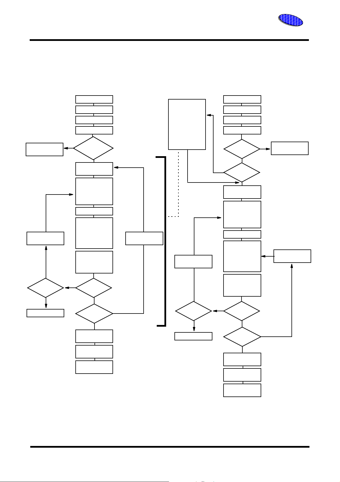
In-System Protection / Unprotection Method
START
COUNT = 1
RESET# = V
Wait 1us
First Write
Cycle = 60h?
Yes
Wait 150us
Verify Se ctor
Protect:
A0 = 0
A0 = 0
Data = 01h?
Protect another
sector?
No
Remove VID
from RESET#
Write reset
command
complete
Protect all sectors:
The indicated portion of the sector
ID
Reset
COUNT = 1
Yes
protect algorithm
must be performed
for all unprotected
sectors prior to
issuing the first
sector unprotect
address
Increment
COUNT
No
COUNT
=1000?
Yes Yes
Device failed
No
No
START
COUNT = 1
RESET# = V
Wait 1us
First Write
Cycle = 60h?
All sectors
protected ?
Set up first sector
address
Sector Unprotect:
Write 60h to sector address with
A6 = 1, A1 = 1,
Wait 15ms
Verify Se ctor
Unprotect:
Write 40h to sector address with
A6 = 1, A1 = 1,
A0 = 0
Read from sector address with
A6 = 1, A1 = 1,
A0 = 0
Data = 00h?
Last sector
verified?
Remove VID from
RESET#
Write reset
command
Yes
Yes
Yes
ID
No
Temporary Sector
Unprotect Mode
Set up next
sector address
No
Figure 3. In-System Sector
Protect Algorithm
ES29LV320D
17
Sector Unprotect
complete
Figure 4. In-System Sector
Unprotect Algorithm
Rev. 2D Jan 5, 2006
ESI
ESI
Excel Semiconductor inc.
A9 High-Voltage Method
Start
Start
COUNT = 1
SET A9=OE#=V
ID
Note: All sectors must be
previously protected.
COUNT = 1
SET A9=OE#=V
ID
Increase COUNT
No
COUNT= 25?
Yes
Device failed
CE#,OE#,A6,A0=V
RESET#, A1 = V
No
Set Sector Address
A<20 :12>
CE#, A6, A0=V
RESET#, A1=V
SET WE# = V
Wait 150 us
SET WE# = V
Read Data
Data = 01h?
Protect Another
Sector ?
Remove VID from
A9 and Write
Reset Command
IL
IH
IL
IH
IH
Yes
No
CE#, A0=V
RESET#,
A6, A1=V
SET WE# = V
Wait 15ms
SET WE# = V
Increase COUNT
IL
No
COUNT=1000?
Yes
Yes
Device failed
CE#,OE#, A0=V
RESET#, A6, A1=V
Set Sector AddressA<20 :12>
Read Data
No
Data = 00h?
Yes
The Last Sector
Address ?
Remove VID from A9 and
Write Reset Command
IH
Yes
,
IL
IL
IH
IL
IH
Increase Sector
Address
No
Sector Protection
Complete
Figure 5. Sector Protection Algorithm
(A9 High-Voltage Method)
ES29LV320D
18
Sector Unprotection
Complete
Figure 6. Sector Un-Protection Algorithm
(A9 High-Voltage Method)
Rev. 2D Jan 5, 2006
ESI
ESI
Excel Semiconductor inc.
Common Flash Memory
Interface (CFI)
CFI is supported in the ES29LV320 device. The
Common Flash Interface (CFI) specification outlines device and host system software interrogation
handshake, which allows specific vendor-specified
software algorithms to be used for entire families of
devices. Software support can then be device-independent, JEDEC ID-independent, and forward- and
backward-compatible for the specified flash device
families. Flash vendors can standardize their existing interfaces for long-term compatibility.
Table 5. CFI Query Identification String
Addresses
(Word Mode)
10h
11h
12h
13h
14h
15h
16h
17h
18h
19h
1Ah
Addresses
(Byte Mode)
20h
22h
24h
26h
28h
2Ah
2Ch
2Eh
30h
32h
34h
Data Description
0051h
0052h
0059h
0002h
0000h
0040h
0000h
0000h
0000h
0000h
0000h
This device enters the CFI Query mode when the
system writes the CFI query command, 98h, to
address 55h in word mode (or address AAh in byte
mode), any time the device is ready to read array
data. The system can read CFI information at the
addresses given in Tables 5-8. To termin ate reading
CFI data, the system must write the reset com-
mand.The CFI query command can be written to the
system when the device is in the autoselect mode
or the erase-suspend-read mode. The device
enters the CFI query mode, and the system can read
CFI data at the addresses given in Tables 5-8.
When the reset command is written, the device
returns respectively to the read mode or erase-suspend-read mode.
Query Unique ASCII string “QRY”
Primary OEM Command Set
Address for Primary Extended Table
Alternate OEM Command Set(00h = none exists)
Address for Alternate OEM Extended Table (00h = none exists)
Table 6. System Interface String
Addresses
(Word Mode)
1Bh 36h 0027h
1Ch 38h 0036h
1Dh 3Ah 0000h Vpp Min. voltage (00h = no Vpp pin present)
1Eh 3Ch 0000h Vpp Max. voltage (00h = no Vpp pin present)
1Fh 3Eh 0004h
20h 40h 0000h
21h 42h 000Ah
22h 44h 0000h
23h 46h 0005h
24h 48h 0000h
25h 4Ah 0004h
26h 4Ch 0000h
Addresses
(Byte Mode)
Data Description
Vcc Min. (write/erase)
D7-D4: volt, D3-D0: 100 millivolt
Vcc Max. (write/erase)
D7-D4: volt, D3-D0: 100 millivolt
Typical timeout per single byte/word write 2
Typical timeout for Min. size buffer write 2
Typical timeout per individual block erase 2
Typical timeout for full chip erase 2
Max. timeout for byte/word write 2
Max. timeout for buffer write 2
Max. timeout per individual block erase 2
Max. timeout for full chip erase 2
N
N
times typical
N
times typical (00h = not supported)
N
N
us (00h = not supported)
N
N
ms (00h = not supported)
times typical
N
times typical
us
ms
ES29LV320D
19
Rev. 2D Jan 5, 2006

Table 7. Device Geometry Definition
ESI
ESI
Excel Semiconductor inc.
Addresses
(Word Mode)
27h 4Eh 0016h
28h
29h
2Ah
2Bh
2Ch 58h 0002h Number of Erase Block Regions within device
2Dh
2Eh
2Fh
30h
31h
32h
33h
34h
35h
36h
37h
38h
39h
3Ah
3Bh
3Ch
Addresses
(Byte Mode)
50h
52h
54h
56h
5Ah
5Ch
5Eh
60h
62h
64h
66h
68h
6Ah
6Ch
6Eh
70h
72h
74h
76h
78h
Data Description
N
byte
0002h
0000h
0000h
0000h
0007h
0000h
0020h
0000h
003Eh
0000h
0000h
0001h
0000h
0000h
0000h
0000h
0000h
0000h
0000h
0000h
Device Size = 2
Flash Device Interface description
02 = x8, x16 Asynchronous
Max. number of bytes multi-byte write = 2
(00h = not supported)
Erase Block Region 1 Information
Number of identical size erase block = 0007h+1 =8
Erase Block Region 1 Information
Number of identical size erase block = 0020h * 256byte = 8Kbyte
Erase Block Region 2 Information
Number of identical size erase block = 003Eh+1 =63
Erase Block Region 2Information
Number of identical size erase block = 0100h * 256byte = 64Kbyte
Erase Block Region 3 Information
Erase Block Region 3 Information
Erase Block Region 4 Information
Erase Block Region 4 Information
N
ES29LV320D
20
Rev. 2D Jan 5, 2006

Table 8. Primary Vendor-Specific Extended Query
ESI
ESI
Excel Semiconductor inc.
Addresses
(Word Mode)
40h
41h
42h
43h 86h 0031h Major version number, ASCII
44h 88h 0031h Minor version number, ASCII
45h 8Ah 0000h
46h 8Ch 0002h
47h 8Eh 0004h
48h 90h 0001h
49h 92h 0004h
4Ah 94h 0000h
4Bh 96h 0000h
Addresses
(Byte Mode)
80h
82h
84h
Data Description
0050h
0052h
0049h
Query-unique ASCII string “PRI”
Address Sensitive Unlock (Bits 1-0)
0 = Required, 1 = Not required
Silicon Revision Number (Bits 7-2)
Erase Suspend
0 = Not Supported, 1 = To Read Only, 2 = To Read & Write
Sector Protect
0 = Not Supported, X = Number of sectors in per group
Sector Temporary Unprotect
00 = Not Supported, 01 = Supported
Sector Protect/Unprotect scheme
04 = In-System Method and A9 High-Voltage Method
Simultaneous Operation
00 = Not Supported
Burst Mode Type
00 = Not Supported, 01 = Supported
4Ch 98h 0000h
4Dh 9Ah 00B5h
4Eh 9Ch 00C5h
4Fh 9Eh 000Xh
Page Mode Type
00 = Not Supported, 01 = 4 Word Page, 02 = 8 Word Page
ACC(Acceleration) Supply Minimum
00h = Not Supported, D7-D4: Volt, D3-D0: 100mV
ACC(Acceleration) Supply Maximum
00h = Not Supported, D7-D4: Volt, D3-D0: 100mV
Top/Bottom Boot Sector Flag
02h = Bottom Boot Device, 03h = Top Boot Device
ES29LV320D
21
Rev. 2D Jan 5, 2006

COMMAND DEFINITIONS
ESI
ESI
Excel Semiconductor inc.
Writing specific address and data commands or
sequences into the command register initiates
device operations. Table 9 defines the valid register
command sequences. Note that writing incorrect
address and data values or writing them in the
improper sequence may place the device in an
unknown state. A reset command is required to
return the device to normal operation.
All addresses are latched on the falling edge of WE#
or CE#, whichever happens later. All data is latched
on the rising edge of WE# or CE#, whichever happens first. Refer to the AC Characteristics section for
timing diagrams.
READING ARRAY DATA
The device is automatically set to reading array data
after device power-up. No commands are required
to retrieve data. The device is ready to read array
data after completing an Embedded Program or
Embedded Erase algorithm.
After the device accepts an Erase Suspend command, the device enters the erase-suspend-read
mode, after which the system can read data from
any non-erase-suspended sector. After completing a
programming operation in the Erase Suspend mode,
the system may once again read array data with the
same exception. See the Erase Suspend/Erase
Resume Commands section for more information.
The system must issue the reset command to return
the device to the read (or erase-suspend-read)
mode if DQ5 goes high during an active program or
erase operation, or if the device is in the autoselect
mode. See the next section, Reset Command, for
more information.
See also Requirements for Reading Array Data in
the Device Bus Operations section for more information.The Read-Only Operations table provides the
read parameters, and Fig. 18 shows the timing diagram
RESET COMMAND
Writing the reset command resets the device to the
read or erase-suspend-read mode. Address bits are
don’t cares for this command.
The reset command may be written between the
sequence cycles in an erase command sequence
before erasing begins. This resets the device to
which the system was writing to the read mode.
Once erasure begins, however, the device ignores
reset commands until the operation is complete.
The reset command may be written between the
sequence cycles in a program command sequence
before programming begins. This resets the device
to which the system was writing to the read mode. If
the program command sequence is written to a sector that is in the Erase Suspend mode, writing the
reset command returns the device to the erase-suspend-read mode. Once programming begins, however, the device ignores reset commands until the
operation is complete.
The reset command may be written between the
sequence cycles in an autoselect command
sequence. Once in the autoselect mode, the reset
command must be written to return to the read
mode. If the device entered the autoselect mode
while in the Erase Suspend mode, writing the reset
command returns the device to th e erase-suspendread mode.
If DQ5 goes high during a program or erase operation, writing the reset command returns the device to
the read mode (or erase- suspend-read mode if the
device was in Erase-Suspend).
ES29LV320D
22
Rev. 2D Jan 5, 2006
Command Definitions
Table 9. ES29LV320 Command Definitions
ESI
ESI
Excel Semiconductor inc.
Command
Sequence
(Note 1)
Read (Note 6) 1 RA RD
Reset (Note 7) 1 XXX F0
Manufacturer ID
Device ID
Security Sector Fac
tory Protect (Note 9)
Sector Protect Verify
Autoselect (Note 8)
(Note 10)
Enter Security Sector Region
Exit Security Sector Region
Program
Unlock Bypass
Unlock Bypass Program (Note 11) 2 XXX A0 PA PD
Unlock Bypass Reset (Note 12) 2 XXX 90 XXX 00
Chip Erase
Sector Erase
Erase Suspend (Note 13) 1 XXX B0
Erase Resume (Note 14) 1 XXX 30
CFI Query (Note 15)
Word
Byte AAA 555 AAA
Word
Byte AAA 555 AAA X02
Word
Byte AAA 555 AAA X06
Word
Byte AAA 555 AAA (SA)X04
Word
Byte AAA 555 AAA
Word
Byte AAA 555 AAA
Word
Byte AAA 555 AAA
Word
Byte AAA 555 AAA
Word
Byte AAA 555 AAA AAA 555 AAA
Word
Byte AAA 555 AAA AAA 555
Word
Byte AA
First Second Third Fourth Fifth Sixth
Cycles
Addr Data Addr Data Addr Data Addr Data Addr Data Addr Data
555
4
555
4
555
4
555
4
555
3
555
4
555
4
555
3
555
6
555
6
55
1
AA
AA
AA
AA
AA
AA
AA
AA
AA
AA
98
2AA
2AA
2AA
2AA
2AA
2AA
2AA
2AA
2AA
2AA
55
55
55
55
55
55
55
55
55
55
Bus Cycles (Notes 2~5)
555
90 X00 4A
555
90
555
90
555
90
555
88
555
90 XXX 00
555
A0 PA PD
555
20
555
80
555
80
X01
X03
(SA)X02
555
555
(See
Table 2)
99/19
00/01
AA
AA
2AA
2AA
555
55
55 SA 30
10
Legend:
X = Don’t care
RA = Address of the memory location to be read.
RD = Data read from location RA during read operation
PA = Address of the memory location to be programmed.
Addresses latch on the falling edge of the WE# or CE# pulse,
whichever happens later.
Notes:
1. See Table 1 for description of bus operations.
2. All values are in hexadecimal.
3. Except for the read cycle and the fourth cycle of the autoselect
command sequence, all bus cycles are write cycles.
4. Data bits DQ15-DQ8 are don’t care in command sequences,
except for RD and PD
5. Unless otherwise noted, address bits A20-A11 are don’t cares.
6. No unlock or command cycles required when device is in
read mode.
7. The Reset command is required to return to the read mode
(or to the erase-suspend-read mode if previously in Erase
Suspend) when a device is in the autoselect mode, or if DQ5
goes high (while the device is providing status information).
8. The fourth cycle of the autoselect command sequence
is a read cycle. Data bits DQ15-DQ8 are don’t care. See the
Autoselect Command Sequence section for more information.
PD = Data to be programmed at location PA. Data latches on the
rising edge of WE# or CE# pulse, whichever happens first.
SA = Address of the sector to be verified (in autoselect mode) or
erased. Address bits A20-A12 uniquely select any sector.
9. The data is 99h for factory locked and 19h for not factory
locked.
10. The data is 00h for an unprotected sector and 01h for a
protected sector.
11. The Unlock Bypass command is required prior to the Unlock Bypass Program command.
12. The Unlock Bypass Reset command is required to return
to the read mode when the device is in the unlock bypass
mode.
13. The system may read and program in non-erasing sectors,
or enter the autoselect mode, when in the Erase Suspend
mode. The Erase Suspend command is valid only during
a sector erase operation.
14. The Erase Resume command is valid only during the Erase
Suspend mode.
15. Command is valid when device is ready to read array data
or when device is in autoselect mode.
ES29LV320D
23
Rev. 2D Jan 5, 2006

ESI
ESI
Excel Semiconductor inc.
AUTOSELECT COMMAND
The autoselect command sequence allows the host
system to access the manufacturer and device
codes, and determine whether or not a sector is
protected, including information about factorylocked or customer lockable version.
Identifier Code Address Data
Manufacturer ID 00h 4Ah
Device ID 01h F6(T),
Security Sector Factory Protect 03h 99 / 19
Sector Group Protect Verify (SA)02h 00 / 01
Table 9 shows the address and data requirements.
This method is an alternative to “A9 high-voltage
method” shown in Table 2, which is intended for
PROM programmers and require s V
pin A9. The autoselect command sequence may be
written to an address within sector that is either in
the read mode or erase-suspend-read mode. The
auto-select command may not be written while the
device is actively programming or erasing. The
autoselect command sequence is initiated by first
writing two unlock cycles. This is followed by a third
write cycle that contains the autoselect command.
The device then enters the autoselect mode. The
system may read at any address any number of
times without initiating another autoselect command sequence.
Once after the device enters the auto-select mode,
the manufacture ID code ( 4Ah ) can be accessed
by one of two ways. Just one read cycle ( with A6,
A1 and A0 = 0 ) can be used. Or four consecutive
read cycles ( with A6 = 1 and A1, A0 = 0 ) for continuation codes (7Fh) and then another last cycle
for the code (4Ah) (with A6, A1 and A0 = 0) can be
used for reading the manufacturer code.
- 4Ah (one-cycle read)
- 7Fh 7Fh 7Fh 7Fh 4Ah (Five-cycle read)
The system must write the reset command to return
to the read mode (or erase-suspend-read mode if
the device was previously in Erase Suspend).
F9h(B)
on address
ID
SECURITY SECTOR COMMAND
In the ES29LV320 device, the security sector region
(256 bytes) provides a secured data area cont aini ng
a random, sixteen-byte electronic serial number(ESN) or customer’s security codes. The security sector region can be accessed by issuing the
three-cycle Enter Security Sector command
sequence. The device continues to access the
security sector region until the system issues the
four-cycle Exit Security Sector command
sequence. The Exit Security Sector command
sequence returns the device to normal operation.
Table 9 shows the address and data requirements
for both command sequences. Note that the accel-
erated programming function by WP#ACC and
unlock bypass mode are not available when the
device has entered the security sector. Refer to the
Fig. 7 for the security sector operation.
Read Mode
Enter Security
Sector Command
Program, Erase or
Sector Command
Figure 7. Security Sector Operation
Protection
Exit Security
Read Mode
ES29LV320D
24
Rev. 2D Jan 5, 2006
ESI
ESI
Excel Semiconductor inc.
BYTE / WORD PROGRAM
The system may program the device by word or
byte, depending on the state of the BYTE# pin.
Programming is a four-bus-cycle operation. The
program command sequence is initiated by writing
two unlock write cycles, followed by the program
set-up command. The program address and data
are written next, which in turn initiate the Embedded
Program algorithm. The system is not required to
provide further controls or timings. The device automatically provides internally generated program
pulses and verifies the programmed cell margin.
Table 9 shows the address and data requirements
for the byte program command sequence. No te that
the autoselect, commands related with the security
sector, and CFI modes are unavailable while a programming operation is in progress.
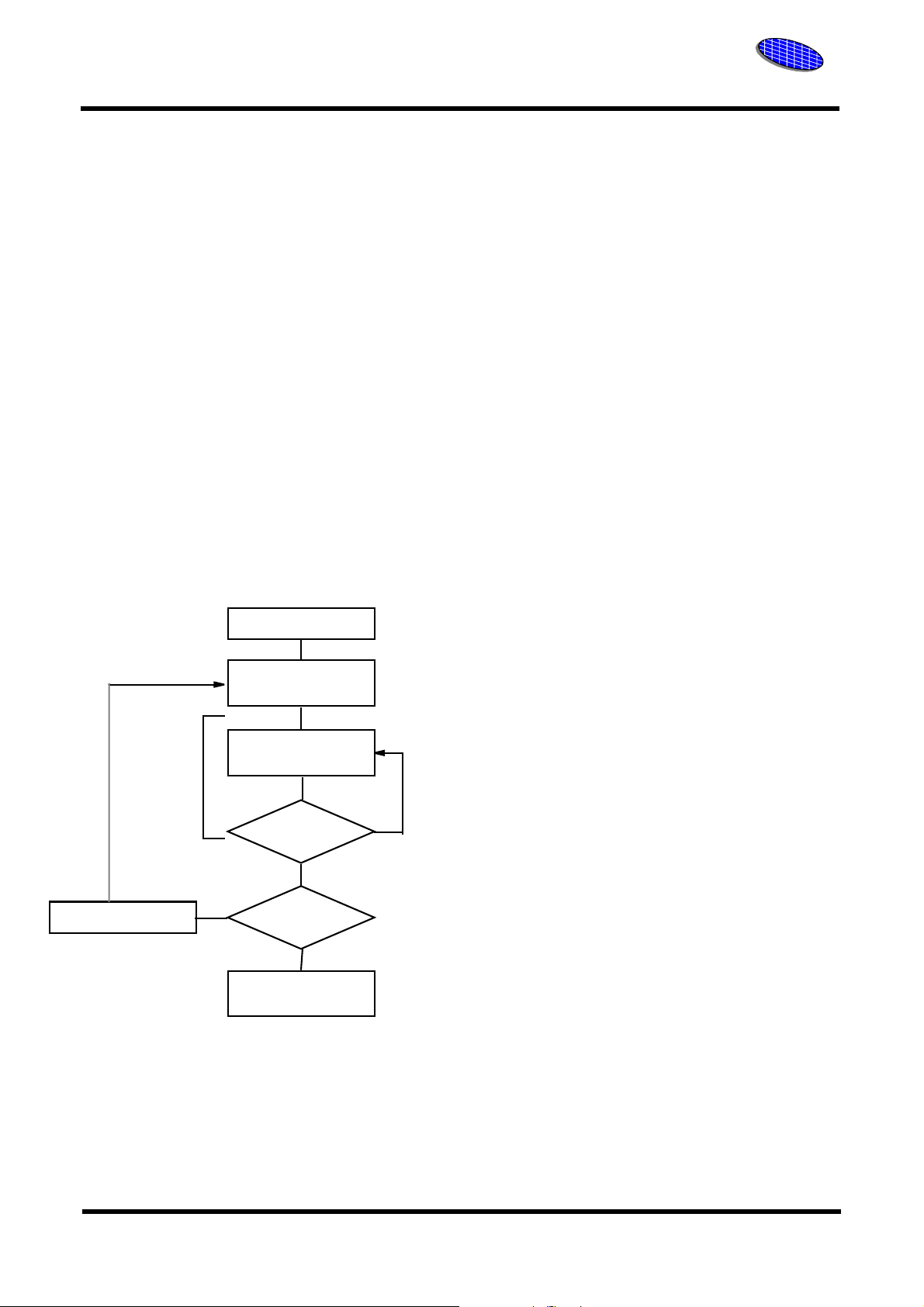
START
Write Program Com-
mand Sequence
Program Status Bits : DQ7, DQ6 or RY/BY#
When the Embedded Program algorithm is complete, the device then returns to the read mode and
addresses are no longer latched. The system can
determine the status of the program operation by
using DQ7, DQ6, or RY/BY#. Refer to the Write
Operation Status section Table 10 for information on
these status bits.
Any Commands Ignored during Programming Operation
Any commands written to the device during the
Embedded Program algorithm are igno red. Note that
a hardware reset can immediately terminates the
program operation. The program command
sequence should be reinitiated once the device has
returned to the read mode, to ensure data integrity.
Programming from “0” back to “1”
Programming is allowed in any sequence and
across sector boundaries. But a bit cannot be programmed from “0” back to a ”1”. Attempting to do so
may cause the device to set DQ5 = 1, or cause the
DQ7 and DQ6 status bits to indicate the operation
was successful. However, a succeeding read will
show that the data is still “0”. Only erase operations
can convert a “0” to a “1”
Embedded
Program
algorithm in
progress
Increment Address
Note:
See Table 9 for program command sequence
Figure 8. Program Operation
Data Poll
from System
Unlock Bypass
In the ES29LV320 device, an unlock bypass program mode is provided for faster programming operation. In this mode, two cycles of program command
sequences can be saved. To enter this mode, an
unlock bypass enter command should be first written
to the system. The unlock bypass enter command
sequence is initiated by first writing two unlock
cycles. This is followed by a third write cycle contain-
No
Verify Data
Last Address?
?
Yes
No
ing the unlock bypass command, 20h. The device
Yes
then enters the unlock-bypass program mode. A
two-cycle unlock bypass program command
Programming
Completed
sequence is all that is required to program in this
mode. The first cycle in this sequence contains the
unlock bypass program set-up command, A0h; the
second cycle contains the program address and
data. Additional data is programmed in the same
manner. This mode dispenses with the initial two
unlock cycles required in the standard program command sequence, resulting in faster total programming time. Table 9 shows the requirements for the
command sequence.
ES29LV320D
25
Rev. 2D Jan 5, 2006

ESI
ESI
Excel Semiconductor inc.
During the unlock-bypass mode, only the unlockbypass program and unlock-bypass reset commands are valid. To exit the unlock-bypass mode,
the system must issue the two-cycle unlock-bypass
reset command sequence. The first cycle must contain the data 90h. The second cycle need to only
contain the data 00h. The device then return s to the
read mode.
- Unlock Bypass Enter Command
- Unlock Bypass Reset Command
- Unlock Bypass Program Command
Unlock Bypass Program during WP#/ACC
Accelerated Program Mode
The device offers accelerated program operations
through the WP#/ACC pin. When the system
asserts V
matically enters the unlock bypass mode. The system may then write the two-cycle unlock bypass
program command sequence. The device uses the
higher voltage on the WP#/ACC pin to accelerate
the operation. Note that the WP#/ACC pin must not
be at V
programming, or device damage may result. In
addition, the WP#/ACC pin must not be left floating
or unconnected; inconsistent behavior of the device
may result. Fig. 8 illustrates the algorithm for the
program operation. Refer to the Erase and Program
Operations table in the AC Characteristics section
for parameters, and Fig. 22 for timing diagrams.
on the WP#/ACC pin, the device auto-
HH
in any operation other than accelerated
HH
CHIP ERASE COMMAND
To erase the entire memory, a chip erase command
is used. This command is a six bus cycle operation.
The chip erase command sequence is initiated by
writing two unlock cycles, followed by a set-up command. Two additional unlock write cycles are then
followed by the chip erase command, which in turn
invokes the Embedded Erase algorithm. The chip
erase command erases the entire memory including all other sectors except the protected sectors,
but the internal erase operation is performed on a
single sector base.
Embedded Erase Algorithm
The device does not require the system to preprogram prior to erase. The Embedded Erase algorithm automatically preprograms and verifies the
entire memory for an all zero data pattern prior to
electrical erase. The system is not required to provide any controls or timings during these operations.
Table 9 shows the address and dat a requ iremen t s fo r
the chip erase command sequence. Note that the
autoselect, security sector, and CFI modes are
unavailable while an erase operation is in progress
Erase Status Bits : DQ7, DQ6, DQ2, or RY/BY#
When the Embedded Erase algorithm is complete,
the device returns to the read mo de and addresses
are no longer latched. The system can determine the
status of the erase operation by using DQ7, DQ6,
DQ2, or RY/BY#. Refer to the Write Operation Status
section Table 10 for information on these status bits.
Commands Ignored during Erase Operation
Any command written during the chip erase operation are ignored. However, note that a hardware reset
immediately terminates the erase operation. If that
occurs, the chip erase command sequence should
be reinitiated once the device has returned to reading
array data. to ensure data integrity. Fig. 9 illustrates
the algorithm for the erase operation. Refer to the
Erase and Program Operations tables in the AC
Characteristics section for parameters, and Fig. 23
section for timing diagrams.
SECTOR ERASE COMMAND
By using a sector erase command, a single sector or
multiple sectors can be erased. The sector erase
command is a six bus cycle operation. The sector
erase command sequence is initiated by writing two
unlock cycles, followed by a set-up command. Two
additional unlock cycles are written, and are then followed by the address of the sector to be erased, and
the sector erase command. Table 9 shows the
address and data requirements for the sector erase
command sequence. Note that the autoselect, security sector, and CFI modes are unavailable while an
erase operation is in progress.
Embedded Sector Erase Algorithm
The device does not require the system to preprogram prior to erase. The Embedded Erase algorithm
automatically programs and verifies the entire memory for an all zero data pattern prior to electrical
erase. The system is not required to pr ovide any controls or timings these operations.
ES29LV320D
26
Rev. 2D Jan 5, 2006

ESI
ESI
Excel Semiconductor inc.
Sector Erase Time-out Window and DQ3
After the command sequence is written, a sector
erase time-out of 50us occurs. During the time-out
period, additional sector addresses and sector
erase commands may be written. Loading the sector erase buffer may be done in any sequence, and
the number of sectors may be from one sector to all
sectors. The time between these additional cycles
must be less than 50 us, otherwise the last addr es s
and command may not be accepted, and erasure
may begin. It is recommend ed that pr ocessor in terrupts be disabled during this time to ensure all commands are accepted. The interrupts can be reenabled after the last Sector Erase command is
written. The system can monitor DQ3 to determine
if the sector erase timer has timed out (See the se ction on DQ3:Sector Erase Timer.). The time-out
begins from the rising edge of the final WE# pulse
in the command sequence.
Any command other than Sector Erase or Erase
Suspend during the time-out period resets the
device to the read mode. The system must rewrite
the command sequence and any additional
addresses and commands.
Status Bits : DQ7,DQ6,DQ2, or RY/BY#
When the Sector Erase Embedded Erase algorithm
is complete, the device returns to reading array data
and addresses are no longer latched. Not e th at while
the Embedded Erase operation is in progress, the
system can read data from the non-erasing sector.
The system can determine the status of the erase
operation by reading DQ7,DQ6,DQ2, or RY/BY# in
the erasing sector. Refer to the Write Operation Status section Table 10 for information on these status
bits.
Valid Command during Sector Erase
Once the sector erase operation has begun, only the
Erase Suspend command is valid. All other commands are ignored. However, note that a hardware
reset immediately terminates the erase operation. If
that occurs, the sector erase command sequence
should be reinitiated once the device has returned to
reading array data, to ensure data integrity.
Fig. 9 illustrates the algorithm for the erase operation. Refer to the Erase and Program Operations
tables in the AC Characteristics section for parameters, and Fig. 23 section for timing diagrams.
START
Write Erase
Command Sequence
(Notes 1,2)
Embedded
Erase
algorithm in
progress
No
Notes:
1. See Table 9 for erase command sequence
2. See the section on DQ3 for information on the sector erase timer
Data Poll to
Erasing Bank
from System
No
Data = FFh?
Yes
Erasure Completed
Figure 9. Erase Operation
ERASE SUSPEND/ERASE RESUME
An erase operation is a long-time operation so that
two useful commands are provided in the
ES29LV320 device Erase Suspend and Erase
Resume Commands. Through the two commands,
erase operation can be suspended for a while and
the suspended operation can be resumed later when
it is required. While the erase is suspend ed, read or
program operations can be performed by the system.
Erase Suspend Command, (B0h)
The Erase Suspend command, B0h, allows the system to interrupt a sector erase operation and then
read data from, or program data to, any sector not
selected for erasure. This command is valid only during the sector erase operation, including the 50us
time-out period during the sector erase command
sequence. The Erase Suspend command is ignored
if written during the chip erase operatio n or Embedded Program algorithm. When the Erase Suspend
command is written during the sector erase operation, the device requires a maximum of 20us to suspend the erase operation. However, when the Erase
Suspend command is written during the sector erase
time-out, the device immediately terminates the timeout period and suspends the erase operation.
ES29LV320D
27
Rev. 2D Jan 5, 2006

Read and Program during Erase-SuspendRead Mode
After the erase operation has been suspended, the
device enters the erase-suspend-read mode. The
system can read data from or program data to any
sector not selected for erasure. (T he device “erase
suspends” all sectors selected for erasure.) Reading
at any address within erase-suspended sectors produces status information on DQ7-DQ0. The system
can use DQ7, or DQ6 and DQ2 together, to determine if a sector is actively erasing or is erase-suspended. Refer to the Write Operation Status section
for information on these status bits (Table 10).
After an erase-suspended program operation is
complete, the device returns to the erase-suspendread mode. The system can determine the status for
the program operation using the DQ7 or DQ6 status
bits, just as in the standard Byte Prog ram operation.
Refer to the Write Operation Status section for more
information.
ESI
ESI
Excel Semiconductor inc.
Autoselect during Erase-Suspend- Read
Mode
In the erase-suspend-read mode, the system can
also issue the autoselected command sequence.
Refer to the Autoselect Mode and Autoselect Command Sequence section for details (Table 9).
Erase Resume Command
To resume the sector erase operation, the system
must write the Erase Resume command. Further
writes of the Resume command are ignored.
Another Erase Suspend command can be written
after the chip has resumed erasing.
ES29LV320D
28
Rev. 2D Jan 5, 2006
ESI
ESI
Excel Semiconductor inc.
COMMAND DIAGRAM
Done
90
Program
Unlock
Bypass
98
CFI
20
90
Autoselect
F0
F0
PA/PD
A0
55
AA
Read
88
80
00
Security
Sector
AA
55
90
Done
AA
Chip
Erase
10
50us
55
SA/30
SA/30
00
98
Erasesuspend
Read
Figure 10. Command Diagram
Done
Resume
30
Sector
Erase
B0
Suspend
ES29LV320D
29
Rev. 2D Jan 5, 2006

WRITE OPERATION STATUS
ESI
ESI
Excel Semiconductor inc.
In the ES29LV320 device, several bits are provided
to determine the status of a program or erase operation: DQ2, DQ3, DQ5, DQ6, DQ7 and RY/BY#.
Table 10 and the following subsections describe the
function of these bits. DQ7 and DQ6 each offer a
method for determining whether a program or erase
operation is complete or in progress. The device
also provides a hardware-based output signal, RY/
BY#, to determine whether an Embedded Program
or Erase operation is in progress or has been completed.
DQ7 (DATA# POLLING)
The Data# Polling bit, DQ7, indicates to the host
system whether an Embedded Program or Erase
algorithm is in progress or complete d, or whether a
device is in Erase Suspend. Data# Polling is valid
after the rising edge of the final WE# pulse in the
command sequence.
During Programming
During the Embedded Program algorithm, the
device outputs on DQ7 the complement of the
datum programmed to DQ7. This DQ 7 status also
applies to programming during Erase Suspend.
When the Embedded Program algorithm is complete, the device outputs the datum programmed to
DQ7. The system must provide the program
address to read valid status information on DQ7. If
a program address falls within a protected sector,
Data# Polling on DQ7 is active for approximately
250ns, then the device returns to the read mode.
During Erase
Erase algorithm is complete, or if the device enters
the Erase Suspend mode, Data# polling produces a
“1” on DQ7. The system must provide an address
within any of the sectors selected for erasure to read
valid status information on DQ7.
Erase on the Protected Sectors
After an erase command sequence is written, if all
sectors selected for erasing are protected, Data#
Polling on DQ7 is active for approximately 1.8us,
then the device returns to the read mode. If not all
selected sectors are protected, the Embedded Erase
algorithm erases the unprotected sectors, and
ignores the selected sectors that are protected.
ever, if the system reads DQ7 at an address within a
protected sector, the status may not be valid.
How-
Data# Polling Algorithm
Just prior to the completion of an Embedded
Program or Ease operation, DQ7 may change
asynchronously with DQ0-DQ6 while Output
Enable(OE#) is asserted low. That is, this device
may change from providing status information to
valid data on DQ7. Depending on when the system
samples the DQ7 output, it may read the status or
valid data. Even if the device has completed the
program or erase operation and DQ7 has valid data,
the data outputs on DQ0-DQ7 will appear on
successive read cycles.
Table 10 shows the outputs for Data# Polling on
DQ7. Fig. 11 shows the Data# Polling algorithm. Fig.
24 in the AC Characteristics section shows the
Data# Polling timing diagram.
During the Embedded Erase algorithm, Data# Polling produces a “0” on DQ7. When the Embedded
ES29LV320D
30
Rev. 2D Jan 5, 2006
ESI
ESI
Excel Semiconductor inc.
Erase Suspend mode. Toggle Bit I may be read at
START
Read DQ7-DQ0
Addr = VA
any address, and is valid after the rising edge of the
final WE# pulse in the command sequence ( prior to
the program or erase operation), and during the sector erase time-out. During an Em bedde d Prog ram or
Erase algorithm operation, successive read cycles to
any address cause DQ6 to toggle. The system may
DQ7 = Data ?
Yes
use either OE# or CE# to control the read cycles.
No
No
DQ5 = 1 ?
When the operation is complete, DQ6 stops toggling.
Yes
Read DQ7-DQ0
Addr = VA
DQ7 = Data ?
FAIL
Notes:
1. VA = Valid address for programming. During a sector erase
operation, a valid address is any sector address within the
sector being erased. During chip erase, a valid address in
any non-protected sector address.
2. DQ7 should be rechecked even if DQ5 = “1” because
DQ7 may change simultaneously with DQ5
Yes
No
PASS
Figure 11. Data# Polling Algorithm
RY/BY# ( READY/BUSY# )
The RY/BY# is a dedicated, open-drain output pin
which indicates whether an Embedded Algorithm is
in progress or complete. The RY/BY# status is valid
after the rising edge of the final W E# pulse in the
command sequence. Since RY/BY# is an opendrain output, several RY/BY# pins can be tied
together in parallel with a pull-up resistor to Vcc. If
the output is low (Busy), the device is actively erasing or programming. (This includes programming in
the Erase Suspend mode.) If the output is high
(Ready), the device is in the read mode, the
standby mode, or in the erase-susp en d- re a d m od e .
Table 10 shows the outputs for RY/BY#.
DQ6 ( TOGGLE BIT I )
Toggle Bit I on DQ6 indicates whether an Embedded Program or Erase algorithm is in progress or
complete, or whether the device has entered the
The system can use DQ6 and DQ2 together to
determine whether a sector is actively erasing or is
erase-suspended. When the device is actively erasing (that is, the Embedded Erase algorithm is in
progress), DQ6 toggles. When the device enters the
Erase Suspend mode, DQ6 stops toggling. However, the system must also use DQ2 to determine
which sectors are erasing or erase-suspended.
Alternatively, the system can use DQ7(see the subsection on DQ7:Data# Polling). DQ6 also toggles
during the erase-suspend-program mode, and stops
toggling once the Embedded Program algorithm is
complete.
Table 10 shows the outputs for Toggle Bit I on DQ6.
Fig. 12 shows the toggle bit algorithm. Fig. 25 in the
“AC Characteristics” section shows the toggle bit
timing diagrams. Fig. 26 shows the differences
between DQ2 and DQ6 in graphical form. See also
the subsection on DQ2 : (Toggle Bit II).
Toggling on the Protected Sectors
After an erase command sequence is written, if all
sectors selected for erasing are pr otected, DQ6 to ggles for approximately 1.8us, then returns to reading
array data. If not all selected sectors are protected,
the Embedded Erase algorithm erases the unprotected sectors, and ignores the selected sectors that
are protected. If a program address falls within a
protected sector, DQ6 toggles for approximately
250ns after the program command sequence is written, then returns to reading array data.
DQ2 ( TOGGLE BIT II )
The “Toggle Bit II” on DQ2, when used with DQ6,
indicates whether a particular sector is actively erasing (that is, the Embedded Erase algorithm is in
progress), or whether that sector is erase-suspended. Toggle Bit II is valid after the rising edge of
the final WE# pulse in the command sequence DQ2
ES29LV320D
31
Rev. 2D Jan 5, 2006

toggles when the system reads at addresses within
those sectors that have been selected for erasure.
(The system may use either OE# or CE# to control
the read cycles.) But DQ2 cannot distinguish
whether the sector is actively erasing or is erasesuspended. DQ6, by comparison, indicates
whether the device is actively erasing, or is in Erase
Suspend, but cannot distinguish which sectors are
selected for erasure. Thus, both status bits are
required for sector and mode information. Refer to
Table 10 to compare outputs for DQ2 and DQ6. Fig.
12 shows the toggle bit algorithm in flowchart fo rm,
and the section “DQ2: Toggle Bit II” explains the
algorithm. See also the DQ6: Toggle Bit I subsection. Fig. 25 shows the toggle bit timing diagram.
Fig. 26 shows how differently DQ2 operates compared with DQ6.
No
START
Read DQ7-DQ0
Read DQ7-DQ0
Toggle Bit
= Toggle ?
Yes
DQ5 = 1 ?
Yes
Read DQ7-DQ0
Twice
ESI
ESI
Excel Semiconductor inc.
No
Reading Toggle Bits DQ6/DQ2
Refer to Fig. 12 for the following discussion. Whenever the system initially begins reading toggle bit
status, it must read DQ7-DQ0 at least twice in a row
to determine whether a toggle bit is toggling. Typically, the system would note and store the value of
the toggle bit after the first read. After the second
read, the system would compare the new value of
the toggle bit with the first. If the toggle bit is not
toggling, the device has completed the program or
erase operation. The system can read array data
on DQ7-DQ0 on the following read cycle. However,
if after the initial two read cycles, the system determines that the toggle bit is still toggling, the system
also should note whether the value of DQ5 is high
(see the section on DQ5). If it is, the system should
then determine again whether the toggle bit is toggling, since the toggle bit may have stopped toggling just as DQ5 went high. If the toggle bit is no
longer toggling, the device has successfully completed the program or erase operation. If it is still
toggling, the device did not completed the operation
successfully, and the system must write the reset
command to return to reading array data. The
remaining scenario is that the system initially determines that the toggle bit is toggling and DQ5 has
not gone high. The system may continue to monitor
the toggle bit and DQ5 through successive read
cycles, determining the status as described in the
previous paragraph. Alternatively, it may choose to
perform other system tasks. In this case, this system must start at the beginning of the algorithm
when it returns to determine the st atus of the oper ation (top of Fig. 12).
Yes
No
Program/Erase
Operation
Complete
Toggle Bit
= Toggle ?
Program/Erase
Operation Not
Complete, Write
Reset Command
Note:
The system should recheck the toggle bit even if DQ5 = “1”
because the toggle bit may stop toggling as DQ5 changes to “1”.
See the subsections on DQ6 and DQ2 for more information.
Figure 12. Toggle Bit Algorithm
ES29LV320D
32
Rev. 2D Jan 5, 2006

ESI
ESI
Excel Semiconductor inc.
DQ5 ( EXCEEDED TIMING LIMITS )
DQ5 indicates whether the program or erase time
has exceeded a specified internal pulse count limit.
Under these conditions DQ5 produces a “1”, indicating that the program or erase cycle was not successfully completed. The device may output a “1”
on DQ5 if the system tries to program a “1” to a
location that was previously programmed to “0”
Only an erase operation can change a “0” back to a
“1”. Under this condition, the device halts the operation, and when the timing limit has been exceeded,
DQ5 produces a ”1”. Under both these conditions,
the system must write the reset command to return
to the read mode.
DQ3 ( SECTOR ERASE TIMER )
After writing a sector erase command sequence,
the system may read DQ3 to determine whether or
not erasure has begun. (The sector erase time
does not apply to the chip erase command.)
If additional sectors are selected for erasure, the
entire time-out also applies after each additional
sector erase command. When the time-out period is
complete, DQ3 switches from a “0” to a”1”. If the
time between additional sector erase commands
from the system can be assumed to be less than
50us, the system need not monitor DQ3. See also
the Sector Erase Command Sequence section. After
the sector erase command is written, the system
should read the status of DQ7 (Data# Polling) or
DQ6 (Toggle Bit I) to ensure that the device has
accepted the command sequence, and then read
DQ3. If DQ3 is “1”, the Embedded Erase algorithm
has begun; all further commands (except Erase Suspend) are ignored until the erasure operation is complete. If DQ3 is “0”, the device will accept additional
sector erase commands. To ensure the command
has been accepted, the system software should
check the status of DQ3 prior to and following each
subsequent sector erase command. If DQ3 is high
on the second status check, the last command might
not have been accepted. In Table 10, DQ3 status
operation is well defined and summarized with other
status bits, DQ7, DQ6, DQ5, and DQ2.
Table 10. Write Operation Status
DQ7
(Note 2)
1 No toggle 0 N/A Toggle 1
Data Data Data Data Data 1
DQ6
Standard
Mode
Erase Suspend Mode
Status
Embedded Program Algorithm DQ7# Toggle 0 N/A No toggle 0
Embedded Erase Algorithm 0 Toggle 0 1 Toggle 0
Erase Suspended
Erase-SuspendRead
Erase-Suspend-Program DQ7# Toggle 0 N/A N/A 0
Sector
Non-Erase
Suspended Sector
Notes :
1. DQ5 switches to “1” when an Embedded Program or Embedded Erase operation has exceeded the maximum timing limits. Refer to the
section on DQ5 for more information.
2. DQ7 and DQ2 require a valid address when reading status information. Refer to the appropriate subsection for further details.
DQ5
(Note 1)
DQ3 DQ2
(Note 2)
RY/
BY#
ES29LV320D
33
Rev. 2D Jan 5, 2006

ESI
ESI
Excel Semiconductor inc.
ABSOLUTE MAXIMUM RATINGS
Storage Temperature
Plastic Packages ..............................................-65
Ambient Temperature
with Power Applied ................ .. ... ... ...................-65
Vo ltage with Respect to Ground
Vcc (Note 1) ..........................................................-0.5V to +4.0V
A9, OE#, RESET# and WP#/ACC (Note 2) ......-0.5V to +12.5V
All other pins (Note 1) ...................................-0.5V to Vcc + 0.5V
Output Short Circuit Current (Note 3) ................. 200 mA
Notes:
1. Minimum DC voltage on input or I/O pins is -0.5V. During voltage
transitions, input or I/O pins may overshoot Vss to -2.0V fo r per iods of up to 20ns. Maximum DC voltage on input or I/O pins is
Vcc+0.5V. See Fig. 13. During voltage transition, input or I/O pins
may overshoot to Vcc+2.0V for periods up to 20ns. See Fig. 13.
2. Minimum DC input voltage on pins A9, OE#, RESET#, and WP#
/ACC is -0.5V. During voltage transitions, A9, OE#, WP#/ACC,
and RESET# may overshoot Vss to -2.0V for periods of up to
20ns. See Fig. 13. Maximum DC input voltage on pin A9 is +12.5V
which may overshoot to +14.0V for periods up to 20ns. Maximum
DC input voltage on WP#/ACC is +9.5V which may overshoot to
+12.0V for periods up to 20ns.
o
C to +150oC
o
C to +125oC
20ns 20ns
+0.8V
Vss-0.5V
Vss-2.0V
20ns
Negative Overshoot
20ns 20ns
Vcc+2.0V
Vcc+0.5V
2.0V
20ns
Positive Overshoot
3. No more than one output may be shorted to ground at a time. Du ration of the short circuit should not be greater than one second.
Stresses above those listed under “Absolute Maximum Ratings” may
cause permanent damage to the device. This is a stress rating only;
functional operation of the device at these or any other conditi ons above those indicated in the operational sections of this datasheet is
not implied. Exposure of the device to absolute maximum ra ting conditions for extended periods may affect device reliability.
OPERATING RANGES
Industrial (I) Devices
Ambient Temperature (T
Commercial Devices
Ambient Temperature (T
Vcc Supply Voltages
Vcc for all devices ............................................2.7V to 3.6V
Vcc for regulated voltage range .....................3.0V to 3.6V
Operating ranges define those limits between which the functionality of the device is guaranteed.
).................................-40oC to +85oC
A
)....................................0oC to +70oC
A
Figure 13. Maximum Overshoot Waveform
ES29LV320D
34
Rev. 2D Jan 5, 2006

DC CHARACTERISTICS
Table 11. CMOS Compatible
ESI
ESI
Excel Semiconductor inc.
Parameter
Symbol
I
LI
I
LIT
I
LR
I
LO
I
CCI
I
CC2
I
CC3
I
CC4
I
CC5
V
IL
V
IH
V
HH
V
ID
V
OL
V
OH1
V
OH2
V
LKO
Parameter Description Test Conditions Min Typ Max Unit
Input Load Current VIN=Vss to Vcc
Vcc=Vcc max
A9 Input Load Current Vcc=Vcc max; A9=12.5V 35 uA
RESET# Input Load Current Vcc=Vcc max; RESET#=12.5V 35 uA
Output Leakage Current Vout=Vss to Vcc,
Vcc=Vcc max
CE#=V
Vcc Active Read Current
(Notes 1,2)
Vcc Active Write Current (Note 2,3) CE#=VIL, OE#=VIH, WE#=V
Vcc Standby Current (Note 2) CE#, RESET#= Vcc+0.3V 0.2 10 uA
Vcc Reset Current (Note 2) RESET#=Vss + 0.3V 0.2 10 uA
Automatic Sleep Mode
(Notes2,4)
Input Low Voltage -0.5 0.8 V
Input High Voltage 0.7xVcc Vcc+0.3 V
Voltage for WP#/ACC Sector
Protect/Unprotect and Program
Acceleration
Voltage for Autoselect and
Temporary Sector Unprotect
Output Low Voltage IOL = 4.0 mA, Vcc = Vcc min 0.45 V
Output High Voltage
Low Vcc Lock-Out Voltage (Note 5) 2.3 2.5 V
CE#=V
OE#=VIH, Byte
IL
mode
, OE#=VIH, Word
IL
mode
VIH = Vcc + 0.3V
= Vss + 0.3V
V
IL
Vcc = 3.0V +
Vcc = 3.0V + 10% 11.5 12.5 V
= -2.0mA, Vcc = Vcc min 0.85 Vcc
I
OH
IOH = -100 uA, Vcc = Vcc min Vcc - 0.4
10% 11.5 12.5 V
5MHz 10 16
1MHz 2 4
5MHz 10 16
1MHz 2 4
IL
+ 3.0 uA
+ 1.0 uA
mA
15 30 mA
0.2 10 uA
V
Notes:
1. The Icc current listed is typically less than 2 mA/MHz, with OE# at V
2. Maximum I
3. Icc active while Embedded Erase or Embedded Program is in progress.
4. Automatic sleep mode enables the low power mode when addresses remain stable for t
200 nA.
5. Not 100% tested.
ES29LV320D
specifications are tested with Vcc = Vcc max.
CC
35
, Typical condition : 25oC, Vcc = 3V
IH
+ 30ns. Typical sleep mode current is
ACC
Rev. 2D Jan 5, 2006
DC CHARACTERISTICS
Zero-Power Flash
25
Icc1 (Active Read current)
20
15
10
Supply Current in mA
5
Icc5 (Automatic Sleep Mode)
ESI
ESI
Excel Semiconductor inc.
Note:
Figure 14. I
12
10
8
6
4
Supply Current in mA
2
0 500 1000 1500 2000 2500 3000 3500 4000
Time in ns
Addresses are switching at 1 MHz
Current vs. Time (Showing Active and Automatic Sleep Currents)
cc1
3.6V
2.7V
0
1
Note:
ES29LV320D
T = 25oC
2
3
Frequency in MHz
Figure 15. Typical I
36
vs. Frequency
cc1
45
Rev. 2D Jan 5, 2006
Device
Under
Test
Figure 16. Test Setup
Note
: Diodes are IN3064 or equivalent
C
L
6.2k
ESI
ESI
Excel Semiconductor inc.
3.3V
Table 12. Test Specifications
Ω
2.7k
Test Condition 80R 90 120
Output Load 1TTL gate
Ω
Output Load Capacitance, C
capacitance)
Input Rise and Fall Times 5 ns
Input Pulse Levels 0.0 - 3.0 V
Input timing measurement reference levels 1.5 V
Output timing measurement reference levels 1.5 V
(including jig
L
30 pF 30 pF 100 pF
Key To Switching Waveforms
WAVEFORM INPUTS OUTPUTS
3.0V
Input
0.0V
1.5V
Steady
Changing from H to L
Changing from L to H
Don’t Care, Any Change Permitted Changing, State Unknown
Does Not Apply Center Line is High Impedance State (High Z)
Output
Measurement Level
1.5V
ES29LV320D
Figure 17. Input Waveforms and Measurement Levels
37
Rev. 2D Jan 5, 2006

AC CHARACTERISTICS
Table 13. Read-Only Operations
ESI
ESI
Excel Semiconductor inc.
Parameter
JEDEC Std. 80R 90 120
t
AVAV
t
AVQV
t
ELQV
t
GLQV
t
EHQZ
t
GHQZ
t
AXQX
Note :
t
RC
t
ACC
t
CE
t
OE
t
DF
t
DF
t
OH
t
OEH
1. Not 100% tested
A
ddress
Read Cycle Time(Note 1) Min 80 90 120 ns
Address to Output Delay CE#,OE#=V
Chip Enable to Output Delay OE#=V
Output Enable to Output Delay Max 35 40 50 ns
Chip Enable to Output High Z (Note 1) Max 16 ns
Output Enable to Output High Z (Note 1) Max 16 ns
Output Hold Time From Addresses, CE# or OE#,
Whichever Occurs First
Output Enable Hold
Time (Note 1)
Description Test Setup
Max 80 90 120 ns
IL
IL
Read Min 0 ns
Toggle and Data# Polling Min 10 ns
t
RC
Max 80 90 120 ns
Min 0 ns
Address Stable
t
ACC
Speed Options Unit
CE#
OE#
WE#
OUTPUTS
RESET#
RY/BY#
0V
t
RH
t
RH
t
OE
t
OEH
t
CE
High-Z
Figure 18. Read Operation Timings
t
OH
Output Valid
t
DF
High-Z
ES29LV320D
38
Rev. 2D Jan 5, 2006

AC CHARACTERISTICS
Table 14. Hardware Reset ( RESET #)
Parameter
JEDEC Std.
t
Ready
t
Ready
t
RP
t
RH
t
RPD
t
RB
RESET# Pin Low (During Embedded Algorithms) to Read Mode
(See Note)
RESET# Pin Low (Not During Embedded Algorithms) to Read
Mode (See Note)
RESET# Pulse Width Min 500 ns
RESET High Time Before Read (See Note) Min 50 ns
RESET# Low to Standby Mode Min 20 us
RY/BY# Recovery Time Min 0 ns
Description All Speed Options Unit
ESI
ESI
Excel Semiconductor inc.
Max 20 us
Max 500 ns
Note :
Not 100% tested
RY/BY#
CE#,OE#
RESET#
RY/BY#
0V
t
RH
t
RP
t
READY
(A) Not During Embedded Algorithm
t
READY
t
RB
CE#,OE#
RESET#
ES29LV320D
t
RP
(B) During Embedded Algorithm
Figure 19. Reset Timings
39
Rev. 2D Jan 5, 2006

AC CHARACTERISTICS
Table 15. Word/Byte Configuration (BYTE#)
Parameter
JEDEC Std.
t
ELFL/tELFH
t
FLQZ
t
FHQV
BYTE#
CE# to BYTE# Switching Low or High Max 5 ns
BYTE# Switching Low to Output HIGH Z Max 30 ns
BYTE# Switching High to Output Active Min 80 90 120 ns
CE#
OE#
ESI
ESI
Excel Semiconductor inc.
Description 80R 90 120 Unit
BYTE# Switching
Switching from
word to byte mode
BYTE# Switching
Switching from
byte to word mode
CE#
DQ
DQ
BYTE#
DQ
DQ
0-DQ14
15/A-1
0-DQ14
15/A-1
t
ELFL
t
ELFH
Data Output
(DQ0-DQ14)
DQ15
Output
t
FLQZ
Data Output
(DQ0-DQ7)
Address Input
t
FHQV
Data Output
(DQ0-DQ7)
Address Input
Data Output
(DQ0-DQ14)
DQ15
Output
Figure 20. BYTE# Timing for Read Operations
The falling edge of the last WE# signal
ES29LV320D
WE#
BYTE#
Note :
t
SET
(tAS)
t
HOLD
(tAH)
Refer to the Erase/Program Operations table for tAS and tAH specifications.
Figure 21. BYTE# Timing for Write Operations
40
Rev. 2D Jan 5, 2006

AC CHARACTERISTICS
Table 16. Erase and Program Operations
Parameter
JEDEC Std.
t
AVAV
t
AVWL
t
WLAX
t
DVWH
t
WHDX
t
GHWL
t
ELWL
t
WHEH
t
WLWH
t
WHDL
t
WHWH1
t
WHWH1
t
WHWH2
t
WC
t
AS
t
ASO
t
AH
t
AHT
t
DS
t
DH
t
OEPH
t
GHWL
t
CS
t
CH
t
WP
t
WPH
t
SR/W
t
WHWH1
t
WHWH1
t
WHWH2
t
VCS
t
RB
t
BUSY
Write Cycle Time (Note 1) Min 80 90 120 ns
Address Setup Time Min 0 ns
Address Setup Time to OE# low during toggle bit polling Min 15 ns
Address Hold Time Min 45 45 50 ns
Address Hold Time From CE# or OE# high during toggle bit polling Min 0 ns
Data Setup Time Min 45 45 50 ns
Data Hold Time Min 0 ns
Output Enable High during toggle bit polling Min 20 ns
Read Recovery Time Before Write (OE# High to WE# Low) Min 0 ns
CE# Setup Time Min 0 ns
CE# Hold Time Min 0 ns
Write Pulse Width Min 35 35 50 ns
Write Pulse Width High Min 30 ns
Latency Between Read and Write Operations Min 0 ns
Programming Operation (Note 2)
Accelerated Programming Operation, Word or Byte (Note 2) Typ 8 us
Sector Erase Operation (Note 2) Typ 0.7 sec
Vcc Setup Time (Note 1) Min 50 us
Write Recovery Time from RY/BY# Min 0 ns
Program/Erase Valid to RY/BY# Delay Max 90 ns
Description 80R 90 120 Unit
Byte Typ 9
Word Typ 1 1
ESI
ESI
Excel Semiconductor inc.
us
Notes:
1. Not 100% tested.
2. See the “Erase And Programming Performance” section for more information.
ES29LV320D
41
Rev. 2D Jan 5, 2006
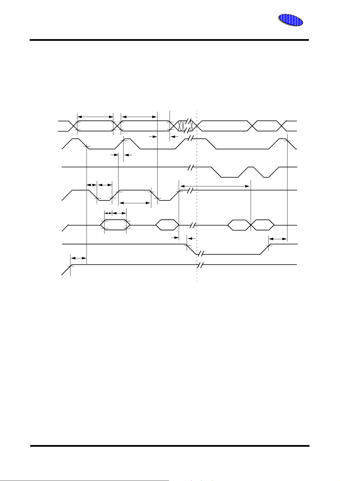
AC CHARACTERISTICS
ESI
ESI
Excel Semiconductor inc.
ddress
A
CE#
OE#
WE#
DATA
RY/BY#
Program Command Sequence (last two cycles)
t
VCS
t
WC
555h
t
CS
t
CH
t
WP
t
DS
A0h PD
t
AS
PA
t
AH
t
WPH
t
DH
t
BUSY
Read Status Data(last two cycles)
t
WHWH1
PA
Status Dout
PA
t
RB
Vcc
NOTES :
1. PA = program address, PD = program data, Dout is the true data at the program address.
2. Illustration shows device in word mode.
Figure 22. Program Operation Timings
ES29LV320D
42
Rev. 2D Jan 5, 2006

AC CHARACTERISTICS
ESI
ESI
Excel Semiconductor inc.
A
ddress
CE#
OE#
WE#
DATA
RY/BY#
Erase Command Sequence (last two cycles)
t
WC
2AAh
t
CS
t
t
CH
WP
t
DS
t
555h for chip erase
t
WPH
t
DH
AS
SA
55h
t
VCS
t
AH
10h for chip erase
30h
t
BUSY
Read Status Data
VA
t
WHWH2
In
Progress
VA
Complete
t
RB
Vcc
NOTES :
1. SA = sector address(for Sector Erase), VA = valid address for reading status data(see “Write Operation Status”).
2. These waveforms are for the word mode.
Figure 23. Chip/Sector Erase Operation Timings
ES29LV320D
43
Rev. 2D Jan 5, 2006

AC CHARACTERISTICS
t
RC
A
ddress
VA VA
t
ACC
t
CE
VA
ESI
ESI
Excel Semiconductor inc.
CE#
OE#
WE#
DQ7
DQ0-DQ6
RY/BY#
NOTE :
t
CH
t
OEH
t
BUSY
VA = Valid address. Illustration shows first status cycle after command sequence, last status read cycle, and array data read cycle
t
OE
t
DF
t
OH
Complement
Status Data
Complement
Status Data
True Valid Data
True
Valid Da ta
HIGH-Z
HIGH-Z
Figure 24. Data# Polling Timings (During Embedded Algorithms)
ES29LV320D
44
Rev. 2D Jan 5, 2006

AC CHARACTERISTICS
ESI
ESI
Excel Semiconductor inc.
A
ddress
CE#
WE#
OE#
DQ6/DQ2
RY/BY#
NOTE :
cycle, and array data read cycle.
VA = Valid address; not required for DQ6. Illustration shows first two status cycle after command sequence, last status read
t
OEH
t
DH
t
AHT
t
ASO
t
OEPH
t
OE
Valid Status Valid Status Valid Status
(first read) (second read) (stops toggling)
t
AHT
t
AS
t
CEPH
Figure 25. Toggle Bit Timings (During Embedded Algorithms)
Valid DataValid Data
Enter
Embedded
Erasing
WE#
DQ6
DQ2
NOTE :
DQ2 and DQ6.
DQ2 toggles only when read at an address within an erase-suspended sector. The system may use OE# or CE# to toggle
ES29LV320D
Erase
Enter
Suspend
Erase
Suspend
Read
Enter Erase
Suspend
Program
Figure 26. DQ2 vs. DQ6
45
Erase
Suspend
Program
Erase
Suspend
Read
Erase
Resume
Erase
Erase
Complete
Rev. 2D Jan 5, 2006
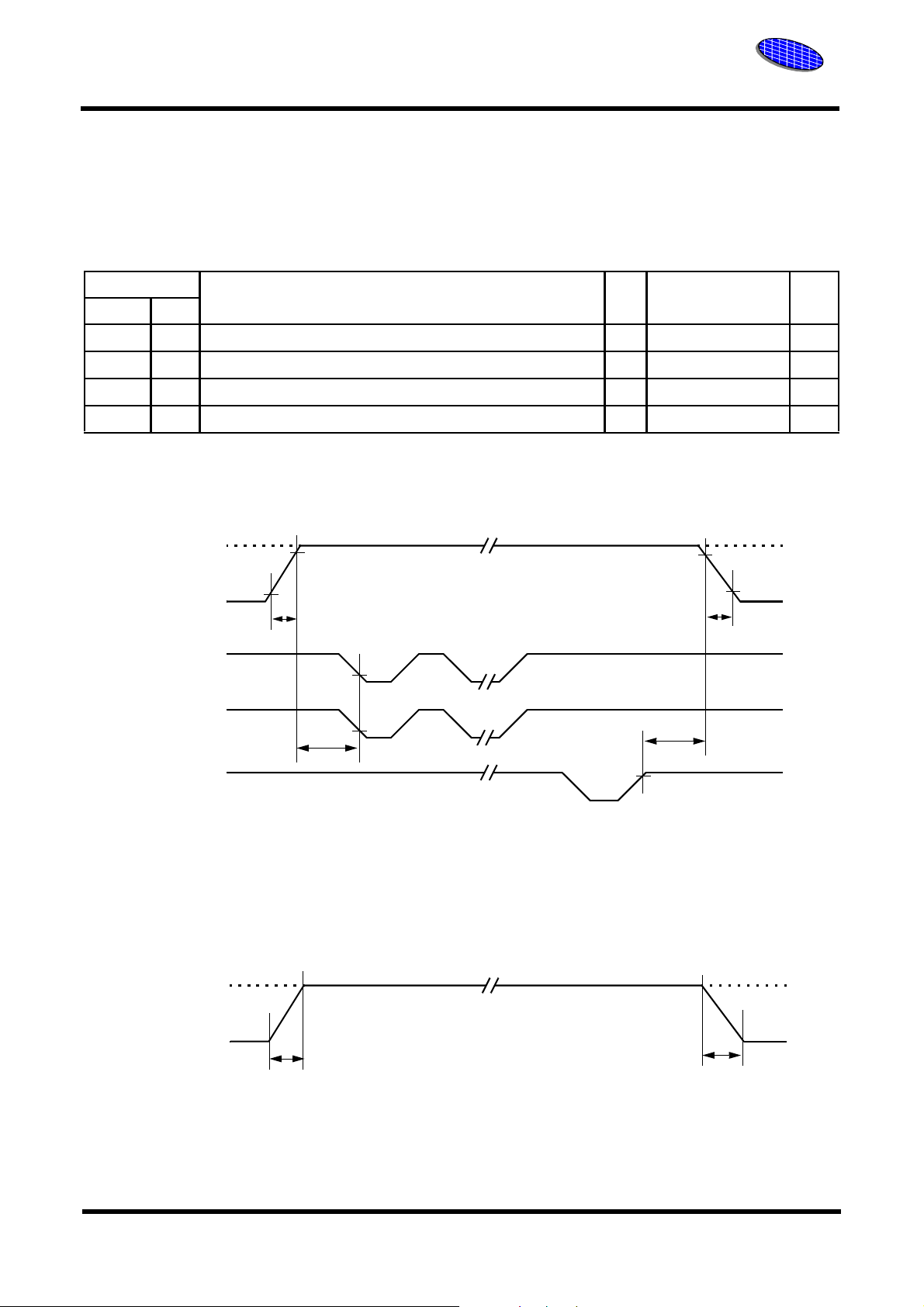
AC CHARACTERISTICS
Table 17. Temporary Sector Unprotect
Parameter
JEDEC Std.
Note:
Not 100% tested.
t
VIDRVID
t
t
t
VHH Rise and Fall Time (See Note) Min 250 ns
VHH
RESET# Setup Time for Temporary Sector Unprotect Min 4 us
RSP
RESET# Hold Time from RY/BY# High for Temporary Sector Unprotect Min 4 us
RRB
Rise and Fall Time (See Note) Min 500 ns
Description All Speed Options Unit
ESI
ESI
Excel Semiconductor inc.
RESET#
CE#
WE#
RY/BY#
V
ID
Vss,VIL,
or V
IH
V
HH
t
VIDR
t
Program or Erase Command Sequence
RSP
t
VIDR
t
RRB
Figure 27. Temporary Sector Unprotect Timing Diagram
WP#/ACC
ES29LV320D
VIL
or V
t
IH
VHH
Figure 28. Accelerated Program Timing Diagram
46
t
VHH
VIL or V
IH
Rev. 2D Jan 5, 2006
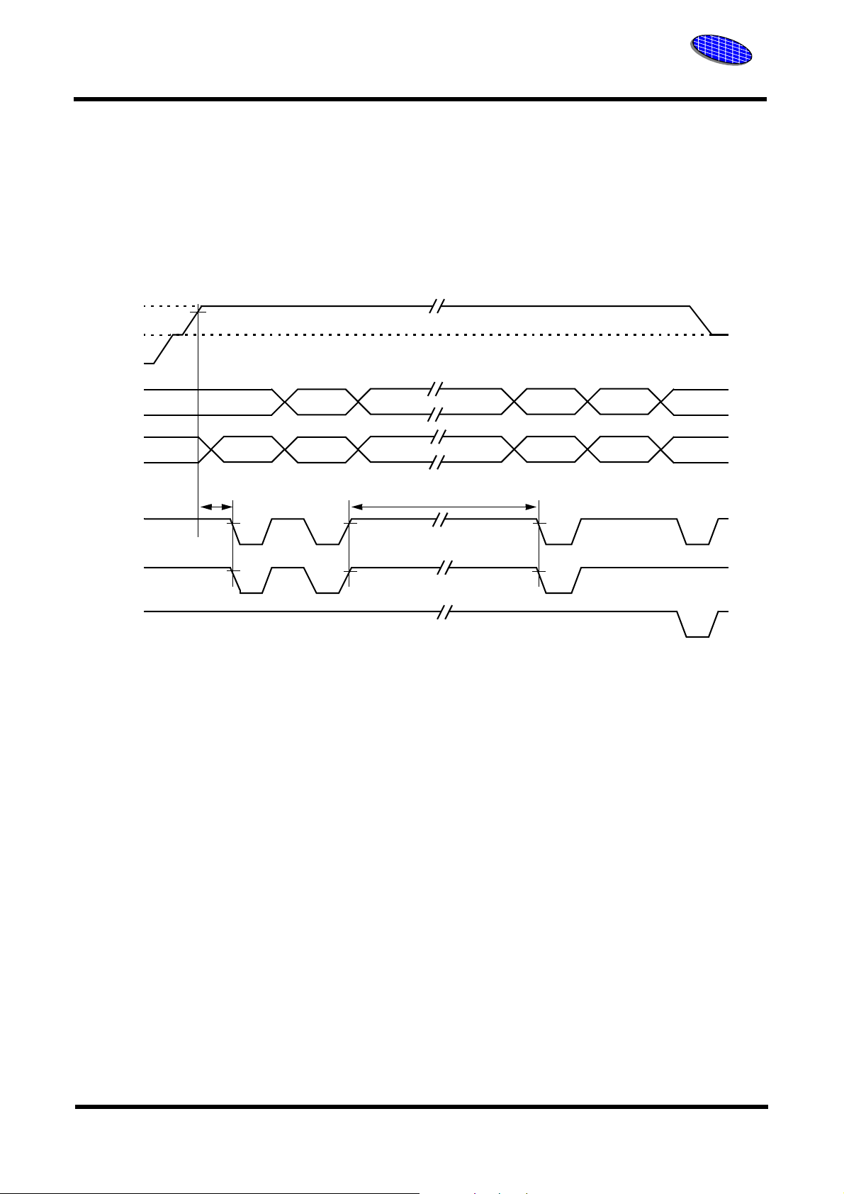
AC CHARACTERISTICS
V
ID
V
IH
RESET#
ESI
ESI
Excel Semiconductor inc.
SA,A6,
A1,A0
DQ
CE#
WE#
OE#
Valid*
Sector/Sector Group Protect or Unprotect
60h 40h
1us
* For sector protect, A6=0,A1=1,A0=0 For sector unprotect, A6=1,A1=1,A0=0
60h
Sector/Sector Group Protect : 150us,
Sector/Sector Group Unprotect: 15ms
Valid* Valid*
Verify
Figure 29. Sector/Sector Group Protect & Unprotect Timing Diagram
Status
ES29LV320D
47
Rev. 2D Jan 5, 2006

AC CHARACTERISTICS
Table 18. Alternate CE# Controlled Erase and Program Operations
ESI
ESI
Excel Semiconductor inc.
Parameter
JEDEC Std.
t
AVAV
t
AVWL
t
ELAX
t
DVEH
t
EHDX
t
GHEL
t
WLEL
t
EHWH
t
ELEH
t
ELEL
t
WHWH1
t
WHWH1
t
WHWH2
t
WC
t
AS
t
AH
t
DS
t
DH
t
GHEL
t
WS
t
WH
t
CP
t
CPH
t
WHWH1
t
WHWH1
t
WHWH2
Write Cycle Time( Note 1) Min 80 90 120 ns
Address Setup Time Min 0 ns
Address Hold Time Min 45 45 50 ns
Data Setup Time Min 45 45 50 ns
Data Hold Time Min 0 ns
Read Recovery Time Before Write (OE# High to WE# Low) Min 0 ns
WE# Setup Time Min 0 ns
WE# Hold Time Min 0 ns
CE# Pulse Width Min 45 45 50 ns
CE# Pulse Width High Min 30 ns
Programming Operation (Note 2)
Accelerated Programming Operation, Word or Byte (Note 2) Typ 8 us
Sector Erase Operation (Note 2) Typ 0.7 sec
Description 80R 90 120 Unit
Byte Typ 9
Word Typ 11
Notes :
1. Not 100% tested
2. See the “Erase And Programming Performance” section for more information.
us
ES29LV320D
48
Rev. 2D Jan 5, 2006

AC CHARACTERISTICS
ESI
ESI
Excel Semiconductor inc.
A
ddress
WE#
OE#
CE#
DATA
RESET#
RY/BY#
555 for program
2AA for erase
t
WC
t
WS
t
t
RH
t
DS
t
CP
t
WH
GHEL
PD for program
SA for sector erase
555 for chip erase
t
AS
t
CPH
t
DH
A0 for program
55 for erase
t
AH
PD for program
30 for sector erase
10 for chip erase
t
BUSY
Data Polling
t
WHWH1 or 2
PA
DQ7#
D
OUT
NOTES :
1. Figure indicates last two bus cycles of a program or erase operation.
2. PA = program address, SA = sector address, PD = program data
3. DQ7# is the complement of the data written to the device. Dout is the data written to the device.
4. Waveforms are for the word mode.
ES29LV320D
Figure 30. Alternate CE# Controlled
Write(Erase/Program) Operation Timings
49
Rev. 2D Jan 5, 2006

Excel Semiconductor inc.
Table 19. AC CHARACTERISTICS
Parameter Description Value Unit
A
<20:12>
t
OE
t
VIDR
t
WPP1
t
WPP2
t
OESP
t
CSP
t
ST
Output Enable to Output Delay Max 35/40/50 ns
Voltage Transition Time Min 500 ns
Write Pulse Width for Protection Operation Min 150 us
Write Pulse Width for Unprotection Operation Min 15 ms
OE# Setup Time to WE# Active Min 4 us
CE# Setup Time to WE# Active Min 4 us
Voltage Setup Time Min 4 us
SAx
SAy
ESI
ESI
A
<0>
A
<1>
A
<6>
A
<9>
OE#
WE#
CE#
DQ
RESET#
Vcc
t
VIDR
V
ID
t
ST
V
ID
t
t
CSP
OESP
t
WPP1
t
VIDR
t
ST
t
OE
0x01
ES29LV320D
Figure 31. Sector Protection timings (A9 High-Voltage Method)
50
Rev. 2D Jan 5, 2006
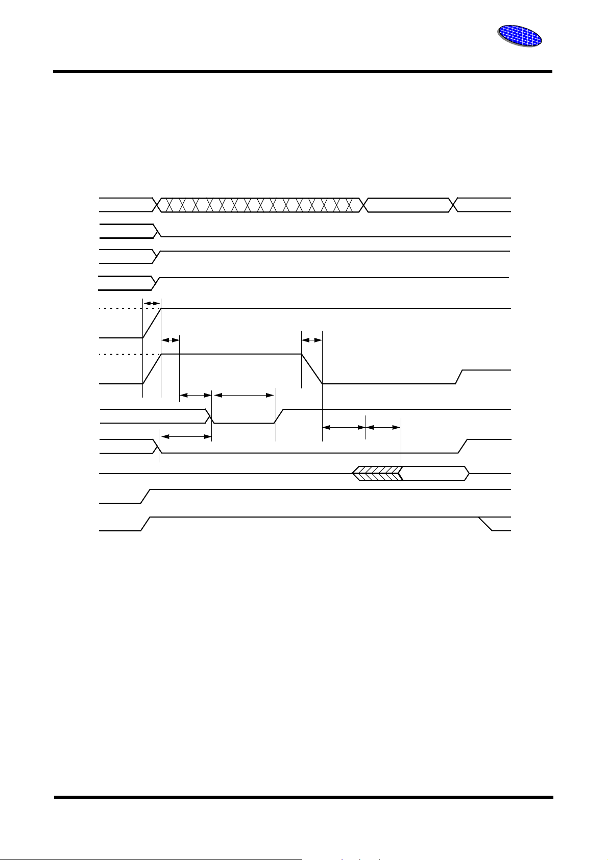
AC CHARACTERISTICS
A
<20:12>
A
<0>
A
<1>
A
<6>
t
VIDR
V
A
<9>
ID
t
ST
t
VIDR
SA0
ESI
ESI
Excel Semiconductor inc.
SA1
OE#
WE#
CE#
DQ
RESET#
Vcc
V
ID
t
NOTE :
OESP
t
CSP
It is recommended to verify for all sectors.
t
WPP2
t
ST
t
OE
Figure 32. Sector Unprotection timings (A9 High-Voltage Method)
0x00
ES29LV320D
51
Rev. 2D Jan 5, 2006

ESI
ESI
Excel Semiconductor inc.
Table 20. ERASE AND PROGRAMMING PERFORMANCE
Parameter T yp (Note 1) Max (Note 2) Unit Comments
Sector Erase Time 0.7 15 sec Excludes 00h programming prior to
Chip Erase Time 112 sec
Byte Program Time 9 300 us
Accelerated Byte/Word Program Time 8 210 us
Word Program Time 11 360 us
Byte Mode 36 108
Chip Program Time (Note 3)
Word Mode 24 72
sec
Notes:
1. Typical program and erase times assume the following conditions: 25oC, 3.0V Vcc, 10,000 cycles. Additionally, programming
typicals assume checkerboard pattern.
2. Under worst case conditions of 90
3. The typical chip programming time is considerably less than the maximum chip programming time listed, since most bytes
program faster than the maximum program times
4. In the pre-programming step of the Embedded Erase algorithm, all bytes are programmed to 00h before erasure.
5. System-level overhead is the time required to execute the two-or-four-bus-cycle sequence for the program command. See
Table 9 for further information on command definitions.
6. The device has a minimum erase and program cycle endurance of 100,000 cycles
o
C, Vcc = 2.7V, 100,000 cycles.
listed.
.
erasure (Note 4)
Exclude system level overhead (Note 5)
Table 21. LATCHUP CHARACTERISTICS
Description Min Max
Input voltage with respect to Vss on all pins except I/O pins (including A9, OE#, and RESET#) - 1.0V 12.5 V
Input voltage with respect to Vss on all I/O pins - 1.0V Vcc + 1.0 V
Vcc Current - 100 mA +100 mA
Note:
Includes all pins except Vcc. Test conditions: Vcc = 3.0 V, one pin at a time
Table 22. TSOP AND BGA PACKAGE CAPACITANCE
Parameter Symbol Parameter Description Test Setup Typ Max Unit
TSOP 6 7.5 pF
C
IN
C
OUT
C
IN2
Notes:
1. Sampled, not 100% tested
2. Test conditions TA = 25
Input Capacitance VIN = 0
Output Capacitance V
Control Pin Capacitance VIN = 0
o
C, f=1.0MHz
.
OUT
= 0
TSOP 8.5 12 pF
TSOP 7.5 9 pF
Table 23. DATA RETENTION
Parameter Description Test conditions Min Unit
Minimum Pattern Data Retention Time
ES29LV320D
52
150
125
o
C
o
C
10 Years
20 Years
Rev. 2D Jan 5, 2006

PHYSICAL DIMENSIONS
48-Pin Standard TSOP (measured in millimeters)
2
N
-B-
5
E
N
---- 1+
2
A
-A-
1
N
----
2
B
B
SEE DETAIL B
D1
D
5
4
SEE DETAIL A
ESI
ESI
Excel Semiconductor inc.
0.10
C
A2
e
9
A1
-C-
SEATING
PLANE
0.08MM (0.0031”)
b
(c)
7
M
C
67
c1
A-B S
WITH
PLATING
R
PARALLEL TO
SEATING PLANE
c
θ°
L
GAUGE
PLANE
0.25MM
(0.0098”) BSC
DETAIL A
Package TS 48
JEDEC MO-142 (B) DD
Symbol MIN NOM MAX
A - - 1.20
A1 0.05 - 0.15
A2 0.95 1.00 1.05
b1 0.17 0.20 0.23
b 0.17 0.22 0.27
c1 0.10 - 0.16
c 0.10 - 0.21
D 19.80 20.00 20.20
D1 18.30 18.40 18.50
E 11.90 12.0 0 12.10
e 0.50 BASIC
L 0.50 0.60 0.70
θ
R 0.08 - 0.20
N48
0°
b1
BASE
METAL
SECTION B-B
e/2
-X-
X = A OR B
DETAIL B
NOTES:
1. Controlling dimensions are in millimeters(mm). (Dimensioning
and tolerancing conforms to ANSI Y14.5M-1982)
2. Pin 1 identifier for standard pin out (Die up).
3. Pin 1 identifier for reverse pin out (Die down): Ink or Laser mark
4. To be determined at the seating plane. The seating plane is def ined as the plane of contact that is made when the package lea ds are allowed to rest freely on a flat horizontal surface.
5. Dimension D1 and E do not include mold protrusion. Allowable
mold protrusion is 0.15mm (0.0059”) per side.
6. Dimension b does not include dambar protrusion. Allowable
dambar protrusion shall be 0.08mm (0.0031”) total in excess
of b dimension at max. material condition. Minimum space
between protrusion and an adjacent lead to be 0.07mm
(0.0028”).
7. These dimensions apply to the flat section of the lead between
0.10mm (0.0039”) and 0.25mm (0.0098”) from the lead tip.
8. Lead coplanarity shall be within 0.10mm (0.004”) as measured
from the seating plane.
9. Dimension “e” is measured at the centerline of the leads.
5°3°
ES29LV320D
53
Rev. 2D Jan 5, 2006

ESI
ESI
Excel Semiconductor inc.
ES29LV320D
54
Rev. 2D Jan 5, 2006

ESI
ESI
Excel Semiconductor inc.
ORDERNG INFORMATION
Standard Products
ESI standard products are available in several p ackage and operating ranges. The o rder numbe r (Valid Combination) is formed by a combination of the following:
ES 29 LV 320 X X - XX X X X X
TEMPERATURE RANGE
Blank : Commercial (0oC to + 70oC)
I : Industrial (- 40
Pb-free
C : Pb product
G : Pb-free product
o
C to + 85oC)
PACKAGE TYPE
T : Standard TSOP (48-pin)
W : FBGA (48-ball)
VOLTAGE RANGE
Blank : 2.7 ~ 3.6V
R : 3.0 ~ 3.6V
SPEED OPTION
70 : 70ns 80 : 80ns 90 : 90ns 12 : 120ns
SECTOR ARCHITECTURE
Blank : Uniform sector
T : Top sector
B : Bottom sector
TECHNOLOGY
D : 0.18um E : 0.15um F : 0.13um
ES29LV320D
55
DENSITY & ORGANIZATION
400 : 4M ( x8 / x16) 800 : 8M ( x8 / x16)
160 : 16M ( x8 / x16) 320 : 32M ( x8 / x16)
640 : 64M ( x8 / x16)
POWER SUPPLY AND INTERFACE
F : 5.0V LV : 3.0V
DL : 3.0V, Dual Bank DS : 1.8V, Dual Bank
BDS : 1.8V, Burst mode, Dual Bank
COMPONENT GROUP
29 : Flash Memory
EXCEL SEMICONDUCTOR
Rev. 2D Jan 5, 2006

Product Selection Guide
Industrial Device
ESI
ESI
Excel Semiconductor inc.
Part No.
ES29LV320DT-80RTGI
ES29LV320DT-80RTCI
ES29LV320DB-80RTGI
ES29LV320DB-80RTCI
ES29LV320DT-90TGI
ES29LV320DT-90TCI
ES29LV320DB-90TGI
ES29LV320DB-90TCI
ES29LV320DT-12TGI
ES29LV320DT-12TCI
ES29LV320DB-12TGI
ES29LV320DB-12TCI
Speed
80ns
80ns
80ns
80ns
90ns
90ns
90ns
90ns
120ns
120ns
120ns
120ns
Vcc
3.0 - 3.6V
3.0 - 3.6V
3.0 - 3.6V
3.0 - 3.6V
2.7 - 3.6V
2.7 - 3.6V
2.7 - 3.6V
2.7 - 3.6V
2.7 - 3.6V
2.7 - 3.6V
2.7 - 3.6V
2.7 - 3.6V
Boot Sector
Top
Top
Bottom
Bottom
Top
Top
Bottom
Bottom
Top
Top
Bottom
Bottom
Package
48-pin TSOP
48-pin TSOP
48-pin TSOP
48-pin TSOP
48-pin TSOP
48-pin TSOP
48-pin TSOP
48-pin TSOP
48-pin TSOP
48-pin TSOP
48-pin TSOP
48-pin TSOP
Pb
Pb-free
-
Pb-free
-
Pb-free
-
Pb-free
-
Pb-free
-
Pb-free
-
Ball Pitch/Size
Body Size
ES29LV320D
56
Rev. 2D Jan 5, 2006

Product Selection Guide
Commercial Device
ESI
ESI
Excel Semiconductor inc.
Part No.
ES29LV320DT-80RTG
ES29LV320DT-80RTC
ES29LV320DB-80RTG
ES29LV320DB-80RTC
ES29LV320DT-90TG
ES29LV320DT-90TC
ES29LV320DB-90TG
ES29LV320DB-90TC
ES29LV320DT-12TG
ES29LV320DT-12TC
ES29LV320DB-12TG
ES29LV320DB-12TC
Speed
80ns
80ns
80ns
80ns
90ns
90ns
90ns
90ns
120ns
120ns
120ns
120ns
Vcc
3.0 - 3.6V
3.0 - 3.6V
3.0 - 3.6V
3.0 - 3.6V
2.7 - 3.6V
2.7 - 3.6V
2.7 - 3.6V
2.7 - 3.6V
2.7 - 3.6V
2.7 - 3.6V
2.7 - 3.6V
2.7 - 3.6V
Boot Sector
Top
Top
Bottom
Bottom
Top
Top
Bottom
Bottom
Top
Top
Bottom
Bottom
Package
48-pin TSOP
48-pin TSOP
48-pin TSOP
48-pin TSOP
48-pin TSOP
48-pin TSOP
48-pin TSOP
48-pin TSOP
48-pin TSOP
48-pin TSOP
48-pin TSOP
48-pin TSOP
Pb
Pb-free
-
Pb-free
-
Pb-free
-
Pb-free
-
Pb-free
-
Pb-free
-
Ball Pitch/Size
Body Size
ES29LV320D
57
Rev. 2D Jan 5, 2006

Document Title
32M Flash Memory
Revision History
Revision Number Data Items
Rev. 0A Nov. 10, 2003 Initia l Rele as e Version.
1. The typical program/erase current valu e changed from 30mA to
15mA.
ESI
ESI
Excel Semiconductor inc.
Rev. 0B No v. 26, 2003
Rev. 0C Feb. 4, 2004 1. E/W cycle number is changed from 1,000,000 to 100,000.
Rev. 1A M a r. 1, 2004
2. The Table 6 for manufacture ID is changed to 4Ah.
3. The extended temperature range is removed and the commercial temperature range is added.
2. CFI code is changed : 45h : 04h ----> 45h : 00h
1. The format of datasheet is entirely changed and updated
2. 70ns product is removed
3. 80R product ( 80ns : Vcc = 3.0 ~ 3.6V) is newly added.
4. A command diagram is added.
5. Sector protection / unprotection algorithm by A9 high-voltage
method is described.
6. A limitation to the maximum number of E/W cycles in the Security Sector is described (300 E/W cycles at Max.).
7. A product selection table is added.
8. Test condtions for the typical performance of program/erase :
after 100,000 E/W cycles ----> after 10,000 E/W cycles
Rev. 1B Apr. 23, 2004
ES29LV320D
1. The bias condition of RESET# in Table 1 for A9 high-Voltage is
changed from V
2. The bias condition of A9 in Table 1 for A9 high-Voltage method
is added.
58
ID
to H.
Rev. 2D Jan 5, 2006

Document Title
32M Flash Memory
Revision History
Revision Number Data Items
1. The preliminary is removed from the datasheet.
2. The Icc3 (max) is changed from 5uA to 10uA.
3. The Icc4 (max) is changed from 5uA to 10uA.
4. The Icc5 (max) is changed from 5uA to 10uA.
ESI
ESI
Excel Semiconductor inc.
Rev. 2A Dec. 1, 2004
Rev. 2B Dec. 13, 2004
Rev. 2C Apr. 1, 2005 1. Remove FBGA Package Type.
Rev. 2D Jan. 5, 2005 1. Add RoHS-Compliant Package Option.
5. The size of FBGA is changed from 8mm x 9mm to 7mm x 8mm.
6. The overall thickness of FBGA , A (max), is ch ang ed fr om 1 . 20
to 1.10. Therefore, ball height (A1) and body thickness (A2)
also is changed accordingly.
7. The ball diameter of FBGA, b(min), b(nom), b(max), is changed
from 0.25, 0.30, and 0.35 to 0.30, 0.35, and 0.40 respectively.
1. The arrow from Erase Suspend Read to Read is changed to
Sector Erase.
2. V
(min), 2.3V is added
LKO
Excel Semiconductor Inc.
1010 Keumkang Hightech Valley , Sangdaewon1-Do ng 133-1, Jungwo n-Gu, Se ongnam- Si, Kyongki-Do , Rep.
of Korea.
The
ifications and products. ESI will answer to your questions about device. If you have any questions, please
ESI office.
ES29LV320D
Zip Code : 462-807 Tel : +82-31-777-5060 Fax : +82-31-740-3798 / Homepage : www.excelsemi.com
attached datasheets are provided by Excel Semiconductor .inc (ESI). ESI reserves the right to change the spec-
contact the
59
Rev. 2D Jan 5, 2006
 Loading...