

Excelics EPA160A Datasheet
Excelics
EPA160A
DATA SHEET
High Efficiency Heterojunction Power FET
+31.0dBm TYPICAL OUTPUT POWER
•
8.5dB TYPICAL POWER GAIN AT 18GHz
•
0.3 X 1600 MICRON RECESSED
•
“MUSHROOM” GATE
PASSIVATION
Si
•
3N4
ADVANCED EPITAXIAL HETEROJUNCTION
•
PROFILE PROVIDES EXTRA HIGH POWER
EFFICIENCY, AND HIGH RELIABILITY
Idss SORTED IN 40mA PER BIN RANGE
•
DDDD
GGGG
SSS
40
95
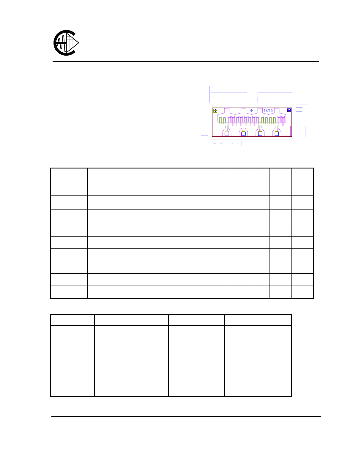
Chip Thickness: 75 ± 13 microns
All Dimensions In Microns
840
116
50
48
340
SS
50
80
100
ELECTRICAL CHARACTERISTICS (Ta = 25 OC)
SYMBOLS PARAMETERS/TEST CONDITIONS MIN TYP MAX UNIT
P
1dB
G
1dB
PAE
Output Power at 1dB Compression f=12GHz
Vds=8V, Ids=50% Idss f=18GHz
Gain at 1dB Compression f=12GHz
Vds=8V, Ids=50% Idss f=18GHz
Power Added Efficiency at 1dB Compression
Vds=8V, Ids=50% Idss f=12GHz
29.0 31.0
31.0
9.5 11.5
8.5
45
dBm
dB
%
Idss
Gm
Vp
BVgd
BVgs
Rth
Saturated Drain Current Vds=3V, Vgs=0V 290 480 660 mA
Transconductance Vds=3V, Vgs=0V 320 500 mS
Pinch-off Voltage Vds=3V, Ids=4.5mA -1.0 -2.5 V
Drain Breakdown Voltage Igd=1.6mA -11 -15 V
Source Breakdown Voltage Igs=1.6mA -7 -14 V
Thermal Resistance (Au-Sn Eutectic Attach) 30
MAXIMUM RATINGS AT 25OC
SYMBOLS PARAMETERS ABSOLUTE1 CONTINUOUS2
Vds
Vgs
Ids
Igsf
Pin
Tch
Tstg
Pt
Note: 1. Exceeding any of the above ratings may result in permanent damage.
2. Exceeding any of the above ratings may reduce MTTF below design goals.
Drain-Source Vo ltage
Gate-Source Voltage
Drain Current
Forward Gate Current
Input Power
Channel Temperature
Storage Temperature
Total Power Dissipation
12V
-8V
Idss
80mA
28dBm
175oC
-65/175oC
4.5W
8V
-3V
475mA
14mA
@3dB Compression
150oC
-65/150oC
3.8W
Excelics Semiconductor, Inc., 2908 Scott Blvd., Santa Clara, CA 95054
Phone: (408) 970-8664 Fax: (408) 970-8998 Web Site: www.excelics.com
o
C/W
EPA160A
DATA SHEET
High Efficiency Heterojunction Power FET
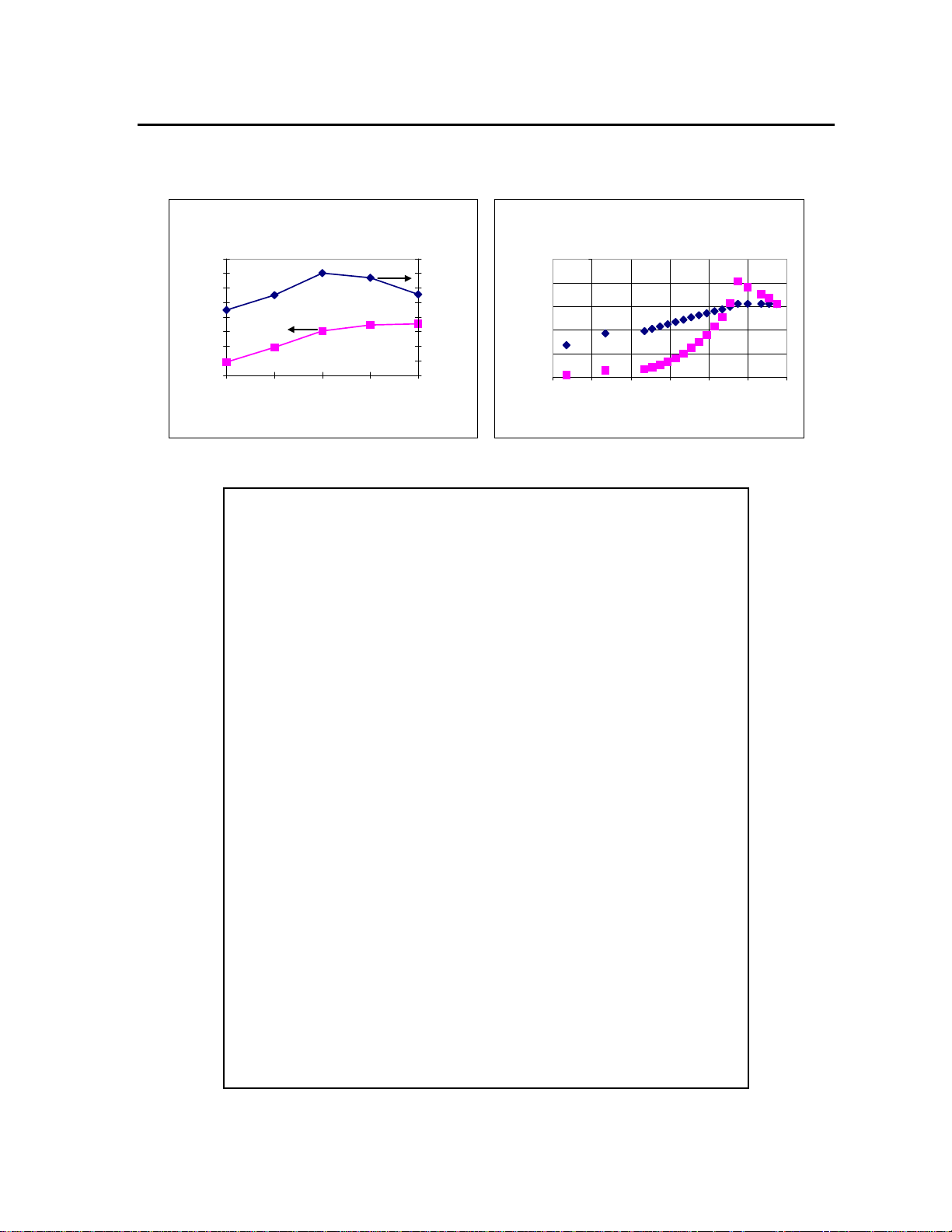
P-1dB & PAE vs. Vds
f = 12 GHz
Ids = 50% Idss
40
38
36
34
32
30
28
P-1dB (dBm )
26
24
45678
Drain-Source Voltage (V)
50
45
40
35
30
25
PAE (%)
20
15
10
50
40
30
20
10
Pout (dBm) or PAE (%)
0
Pout & PAE vs. Pin
f = 12 GHz
Vds = 8V, Ids = 50% Idss
PAE
Pout
-5 0 5 10 15 20 25
Pin (dBm)
S-PARAMETERS
8V, 1/2 Idss
FREQ --- S11 --- --- S21 --- --- S12 --- --- S22 ---
(GHz) MAG ANG MAG ANG MAG ANG MAG ANG
1.0 0.891 -118.3 14.073 114.9 0.028 32.7 0.344 -141.1
2.0 0.890 -146.2 7.912 96.6 0.031 22.3 0.385 -156.6
3.0 0.889 -157.7 5.382 86.8 0.031 20.5 0.401 -162.4
4.0 0.892 -163.6 4.093 79.3 0.032 19.1 0.416 -164.1
5.0 0.887 -167.5 3.275 73.1 0.031 21.8 0.431 -164.8
6.0 0.893 -170.0 2.741 67.3 0.031 24.5 0.449 -164.8
7.0 0.898 -171.6 2.341 62.4 0.031 26.6 0.467 -164.9
8.0 0.901 -173.3 2.036 57.4 0.031 27.6 0.485 -164.8
9.0 0.901 -174.1 1.793 53.2 0.029 28.8 0.496 -165.0
10.0 0.906 -174.9 1.604 49.2 0.029 33.3 0.511 -165.2
11.0 0.912 -175.3 1.449 45.1 0.028 35.6 0.526 -166.2
12.0 0.921 -175.9 1.316 40.9 0.029 36.4 0.538 -168.1
13.0 0.929 -176.3 1.202 36.6 0.029 36.0 0.553 -170.8
14.0 0.929 -176.6 1.096 32.2 0.030 36.4 0.564 -174.4
15.0 0.934 -176.7 1.010 27.8 0.030 37.1 0.578 -179.0
16.0 0.929 -176.6 0.920 23.2 0.031 33.7 0.597 175.9
17.0 0.933 -175.9 0.849 19.1 0.031 32.2 0.623 171.0
18.0 0.943 -176.0 0.790 14.4 0.033 30.4 0.652 165.8
19.0 0.943 -176.3 0.731 9.7 0.034 31.5 0.684 161.2
20.0 0.941 -176.7 0.672 5.2 0.036 31.0 0.710 157.2
21.0 0.930 -176.9 0.616 1.7 0.039 31.3 0.734 155.0
22.0 0.925 -177.3 0.578 -1.6 0.042 31.5 0.764 153.3
23.0 0.926 -177.9 0.545 -4.1 0.047 32.0 0.790 152.4
24.0 0.926 -179.1 0.518 -6.9 0.051 33.7 0.807 152.1
25.0 0.906 179.0 0.492 -8.9 0.057 34.8 0.817 152.4
26.0 0.906 178.1 0.471 -10.2 0.064 36.7 0.811 154.7
Note: The data included 0.7 mils diameter Au bonding wires:
4 gate wires, 15 mils each; 4 drain wires, 20 mils each; 10 source wires, 7 mils each.
 Loading...