

Excelics EPA120A Datasheet
Excelics
EPA120A
DATA SHEET
High Efficiency Heterojunction Power FET
+29.5dBm TYPICAL OUTPUT POWER
•
9.5dB TYPICAL POWER GAIN AT 18GHz
•
0.3 X 1200 MICRON RECESSED
•
“MUSHROOM” GATE
PASSIVATION
Si
•
3N4
ADVANCED EPITAXIAL HETEROJUNCTION
•
PROFILE PROVIDES EXTRA HIGH POWER
EFFICIENCY, AND HIGH RELIABILITY
Idss SORTED IN 30mA PER BIN RANGE
•
40
S
95
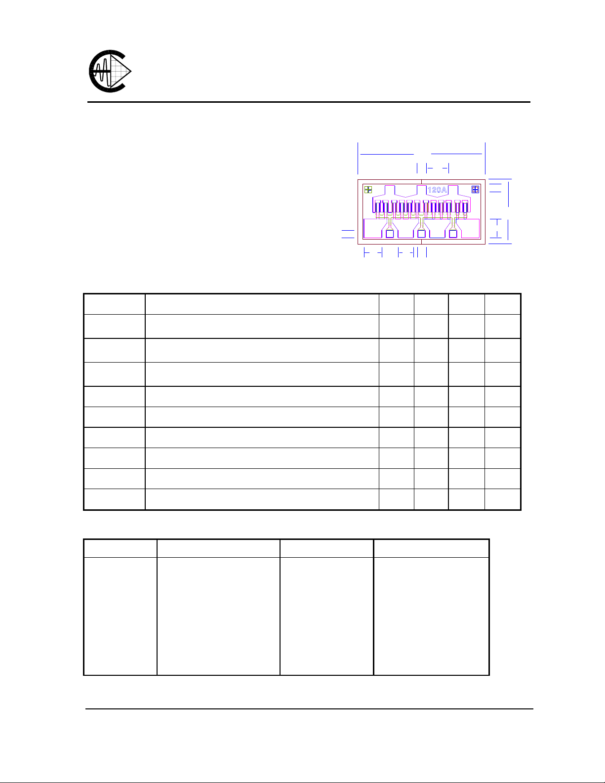
Chip Thickness: 75 ± 13 microns
All Dimensions In Microns
670
116
50
DD
GGG
S
50
80
D
SS
48
340
100
ELECTRICAL CHARACTERISTICS (Ta = 25 OC)
SYMBOLS PARAMETERS/TEST CONDITIONS MIN TYP MAX UNIT
P
1dB
G
1dB
PAE
Output Power at 1dB Compression f=12GHz
Vds=8V, Ids=50% Idss f=18GHz
Gain at 1dB Compression f=12GHz
Vds=8V, Ids=50% Idss f=18GHz
Power Added Efficiency at 1dB Compression
Vds=8V, Ids=50% Idss f=12GHz
28.0 29.5
29.5
10.0 12.0
9.5
45
dBm
dB
%
Idss
Gm
Vp
BVgd
BVgs
Rth
Saturated Drain Current Vds=3V, Vgs=0V 220 360 500 mA
Transconductance Vds=3V, Vgs=0V 240 380 mS
Pinch-off Voltage Vds=3V, Ids=3.5mA -1.0 -2.5 V
Drain Breakdown Voltage Igd=1.2mA -12 -15 V
Source Breakdown Voltage Igs=1.2mA -7 -14 V
Thermal Resistance (Au-Sn Eutectic Attach) 37
MAXIMUM RATINGS AT 25OC
SYMBOLS PARAMETERS ABSOLUTE1 CONTINUOUS2
Vds
Vgs
Ids
Igsf
Pin
Tch
Tstg
Pt
Note: 1. Exceeding any of the above ratings may result in permanent damage.
2. Exceeding any of the above ratings may reduce MTTF below design goals.
Drain-Source Vo ltage
Gate-Source Voltage
Drain Current
Forward Gate Current
Input Power
Channel Temperature
Storage Temperature
Total Power Dissipation
12V
-8V
Idss
60mA
27dBm
175oC
-65/175oC
3.7W
8V
-3V
385mA
10mA
@3dB Compression
150oC
-65/150oC
3.1 W
Excelics Semiconductor, Inc., 2908 Scott Blvd., Santa Clara, CA 95054
Phone: (408) 970-8664 Fax: (408) 970-8998 Web Site: www.excelics.com
o
C/W
EPA120A
DATA SHEET
High Efficiency Heterojunction Power FET
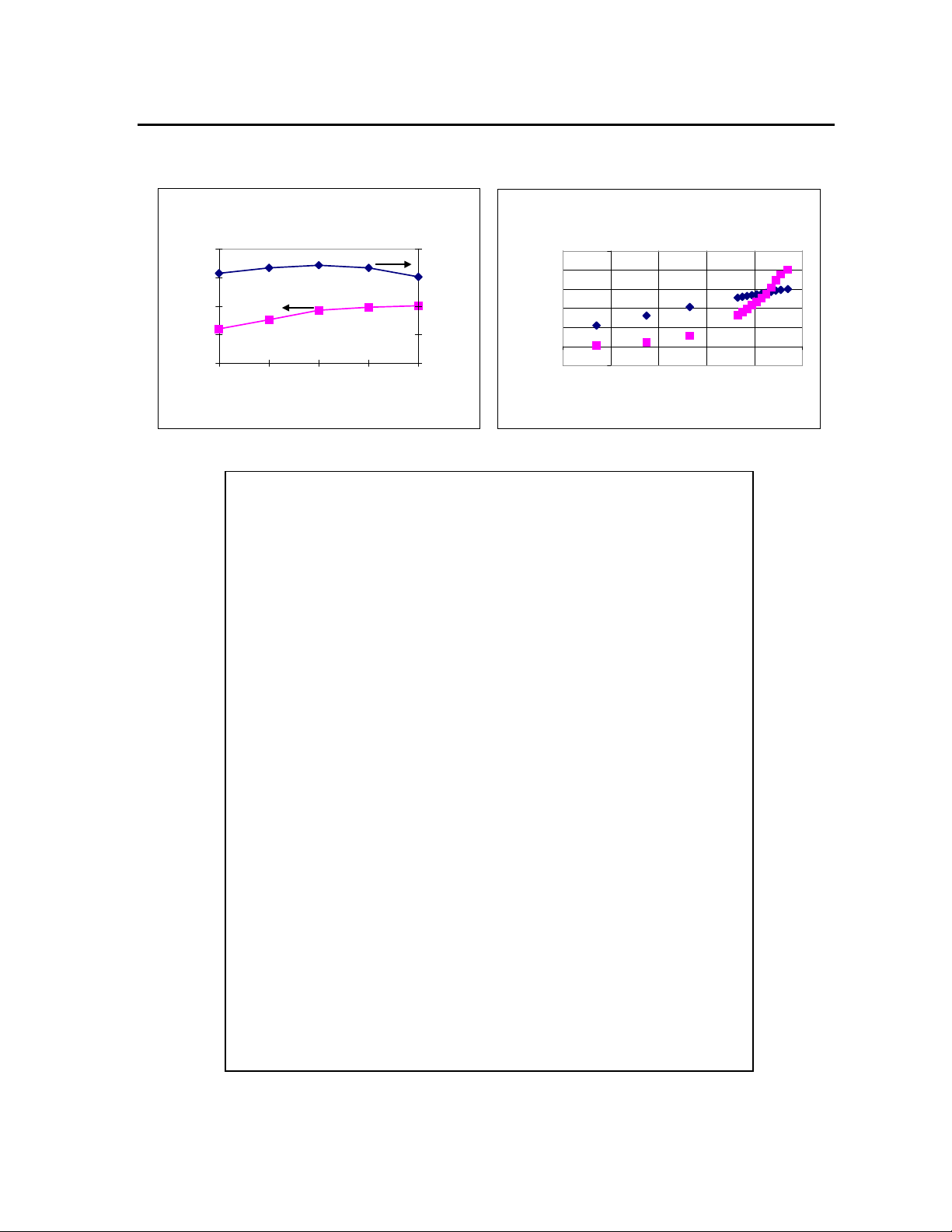
P-1dB & PAE vs. Vds
f = 12 GHz
Ids = 50% Idss
40
35
30
25
P-1dB (dBm)
20
45678
Drain-Source Voltage (V)
50
40
30
PAE (%)
20
10
50
40
30
20
10
0
-10
Pout (dBm) or PAE (%)
Pout & PAE vs. Pin
f = 12 GHz
Vds = 8V, Ids = 50% Idss
Pout
-5 0 5 10 15 20
Pin (dBm)
S-PARAMETERS
8V, 1/2 Idss
FREQ --- S11 --- --- S21 --- --- S12 --- --- S22 --(GHz) MAG ANG MAG ANG MAG ANG MAG ANG
1.0 0.890 -98.0 15.016 124.1 0.029 40.0 0.262 -100.0
2.0 0.878 -132.7 9.107 103.0 0.036 26.8 0.278 -127.9
3.0 0.871 -148.6 6.343 91.3 0.037 20.5 0.290 -138.9
4.0 0.871 -157.2 4.875 82.8 0.037 19.1 0.307 -142.9
5.0 0.865 -163.0 3.927 75.8 0.036 18.9 0.325 -145.1
6.0 0.870 -167.0 3.304 69.5 0.036 20.4 0.345 -146.0
7.0 0.873 -169.9 2.838 64.1 0.036 21.0 0.367 -147.1
8.0 0.878 -173.0 2.483 58.4 0.035 21.0 0.391 -148.0
9.0 0.876 -175.1 2.192 53.7 0.034 21.1 0.407 -149.2
10.0 0.879 -177.1 1.960 49.0 0.032 24.3 0.428 -150.3
11.0 0.885 -178.9 1.774 44.4 0.032 25.5 0.450 -152.0
12.0 0.896 179.2 1.616 39.8 0.032 27.6 0.469 -154.4
13.0 0.904 177.4 1.474 34.9 0.032 27.3 0.490 -157.4
14.0 0.905 175.7 1.343 30.3 0.033 27.3 0.507 -160.9
15.0 0.911 174.5 1.235 25.5 0.033 28.1 0.526 -165.2
16.0 0.906 173.3 1.126 20.7 0.034 27.9 0.551 -169.8
17.0 0.913 172.6 1.044 16.4 0.035 25.9 0.576 -174.1
18.0 0.922 171.3 0.971 11.5 0.036 23.3 0.604 -178.8
19.0 0.925 169.9 0.899 6.6 0.037 25.8 0.637 176.8
20.0 0.920 168.6 0.827 1.8 0.039 24.4 0.663 172.6
21.0 0.910 168.0 0.760 -2.2 0.042 25.1 0.686 169.6
22.0 0.907 166.8 0.715 -5.9 0.045 26.2 0.711 167.1
23.0 0.910 165.7 0.676 -9.1 0.049 27.8 0.736 165.3
24.0 0.911 164.1 0.642 -12.8 0.056 28.2 0.758 163.7
25.0 0.893 161.9 0.600 -15.8 0.060 31.5 0.766 162.5
26.0 0.883 161.5 0.573 -17.2 0.065 31.4 0.763 163.6
Note: The data included 0.7 mils diameter Au bonding wires:
3 gate wires, 15 mils each; 3 drain wires, 20 mils each; 8 source wires, 7 mils each.
PAE
 Loading...