

Excelics EFA080A Datasheet
Excelics
EFA080A
DATA SHEET
Low Distortion GaAs Power FET
+26.0dBm TYPICAL OUTPUT POWER
•
10.0dB TYPICAL POWER GAIN AT 12GHz
•
0.3 X 800 MICRON RECESSED “MUSHROOM” GATE
•
PASSIVATION
Si
•
3N4
ADVANCED EPITAXIAL DOPING PROFILE
•
PROVIDES HIGH POWER EFFICIENCY,
LINEARITY AND RELIABILITY
Idss SORTED IN 15mA PER BIN RANGE
•
ELECTRICAL CHARACTERISTICS (Ta = 25 OC)
SYMBOLS PARAMETERS/TEST CONDITIONS MIN TYP MAX UNIT
P
1dB
G
1dB
PAE
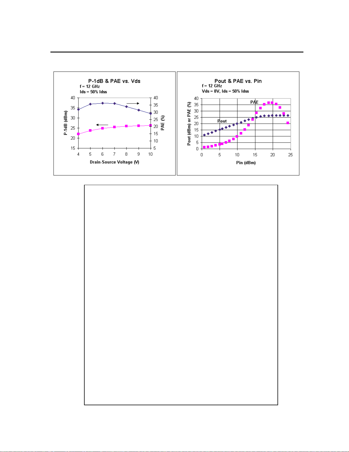
Output Power at 1dB Compression f=12GHz
Vds=8V, Ids=50% Idss f=18GHz
Gain at 1dB Compression f=12GHz
Vds=8V, Ids=50% Idss f=18GHz
Power Added Efficiency at 1dB Compression
Vds=8V, Ids=50% Idss f=12GHz
40
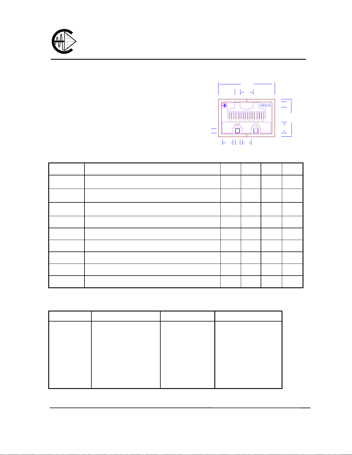
Chip Thickness: 75 ± 13 microns
All Dimensions In Microns
24.0 26.0
510
116
50
D
G
S
5095
8.0 10.0
D
G
SS
80
26.0
7.5
35
48
100
dBm
340
dB
%
Idss
Gm
Vp
BVgd
BVgs
Rth
Saturated Drain Current Vds=3V, Vgs=0V 130 210 300 mA
Transconductance Vds=3V, Vgs=0V 90 120 mS
Pinch-off Voltage Vds=3V, Ids=2.0mA -2.0 -3.5 V
Drain Breakdown Voltage Igd=1.0mA -12 -15 V
Source Breakdown Voltage Igs=1.0mA -7 -14 V
Thermal Resistance (Au-Sn Eutectic Attach) 55
MAXIMUM RATINGS AT 25OC
SYMBOLS PARAMETERS ABSOLUTE1 CONTINUOUS2
Vds
Vgs
Ids
Igsf
Pin
Tch
Tstg
Pt
Note: 1. Exceeding any of the above ratings may result in permanent damage.
2. Exceeding any of the above ratings may reduce MTTF below design goals.
Drain-Source Vo ltage
Gate-Source Voltage
Drain Current
Forward Gate Current
Input Power
Channel Temperature
Storage Temperature
Total Power Dissipation
12V
-8V
Idss
20mA
25dBm
175oC
-65/175oC
2.5 W
8V
-4V
260mA
4mA
@ 3dB Compression
150oC
-65/150oC
2.1 W
Excelics Semiconductor, Inc., 2908 Scott Blvd., Santa Clara, CA 95054
Phone: (408) 970-8664 Fax: (408) 970-8998 Web Site: www.excelics.com
o
C/W
EFA080A
DATA SHEET
S-PARAMETERS
8V, 1/2 Idss
FREQ --- S11 --- --- S21 --- --- S12 --- --- S22 --(GHz) MAG ANG MAG ANG MAG ANG MAG ANG
1.0 0.983 -38.9 6.602 158.2 0.029 65.4 0.421 -24.5
2.0 0.949 -71.6 5.927 135.8 0.050 49.2 0.380 -45.7
3.0 0.916 -96.5 4.998 118.0 0.061 36.4 0.343 -62.4
4.0 0.894 -115.4 4.191 104.1 0.066 27.2 0.326 -75.6
5.0 0.879 -130.5 3.536 92.2 0.068 19.6 0.327 -87.3
6.0 0.873 -140.5 3.028 82.8 0.069 14.5 0.339 -95.6
7.0 0.871 -148.3 2.628 74.6 0.068 10.3 0.359 -102.4
8.0 0.869 -154.1 2.311 67.5 0.067 7.4 0.382 -107.5
9.0 0.872 -158.8 2.058 61.1 0.065 3.8 0.408 -111.9
10.0 0.872 -162.7 1.857 55.2 0.063 3.0 0.433 -115.1
11.0 0.873 -166.5 1.689 49.5 0.061 1.8 0.457 -118.4
12.0 0.876 -169.7 1.557 43.9 0.060 1.0 0.478 -121.4
13.0 0.879 -173.3 1.446 38.4 0.058 -0.9 0.495 -124.4
14.0 0.880 -177.4 1.356 32.9 0.059 -2.3 0.511 -127.6
15.0 0.882 178.3 1.276 27.2 0.057 -2.9 0.522 -131.2
16.0 0.886 173.2 1.207 20.9 0.057 -4.6 0.532 -135.3
17.0 0.889 168.2 1.141 14.6 0.057 -5.7 0.542 -140.3
18.0 0.892 162.8 1.075 8.3 0.058 -7.1 0.557 -145.3
19.0 0.897 157.9 1.010 1.7 0.057 -8.0 0.568 -151.5
20.0 0.905 153.4 0.949 -4.6 0.057 -9.8 0.585 -157.6
21.0 0.923 152.7 0.829 -9.6 0.053 -9.0 0.627 -165.3
22.0 0.928 150.2 0.769 -14.6 0.053 -9.5 0.650 -170.5
23.0 0.936 147.8 0.713 -19.7 0.052 -7.8 0.680 -174.4
24.0 0.939 146.5 0.664 -23.8 0.052 -5.4 0.706 -177.2
25.0 0.945 145.2 0.624 -27.3 0.053 -3.9 0.728 -179.7
26.0 0.944 144.7 0.592 -30.4 0.053 0.4 0.753 179.1
Note: The data included 0.7 mils diameter Au bonding wires:
2 gate wires, 15 mils each; 2 drain wires, 20 mils each; 6 source wires, 7 mils each.
Low Distortion GaAs Power FET
 Loading...