

Exar XRT83SL38/L38EVAL User Manual

XRT83SL38/L38EVAL User Manual
XRT83SL38/L38EVAL
EVALUATION SYSTEM
USER MANUAL
Page 1 of 23
XRT83SL38/L38EVAL User Manual
EVALUATION KIT PART LIST
This kit contains the following:
• XRT83SL38/L38EVAL Application Board
• XRT83SL38/L38 GUI Evaluation Software
• XRT83SL38/L38 128-Pin TQFP
• XRT83SL38/L38EVAL User Manual
• XRT83SL38/L38 Datasheet
FEATURES
• CPLD Design Which Emulates Microprocessor Support for the 8-Bit Parallel Interface
• 25 DIN Connector for Easy Connection Through a Standard Parallel Port to a PC
• CD ROM or Floppy Disk Containing the GUI Software (Executable File)
• Line Interface Modules Coupled to the Receiver Inputs and Transmitter Outputs
• Power Supply Design Allowing a Single 3V Supply voltage
• Accessible I/O Interface for Common Laboratory Equipment
• Optimized layout with Four Layers
INTRODUCTION
The XRT83SL38/L38EVAL is a complete printed circuit board for characterizing Exar’s
XRT83SL38/L38. The XRT83SL38/L38 is a fully integrated four channel, long haul, short haul
line interface unit for T1, E1 or J1 applications.
This application board combines a proven PC board layout with optimized analog and digital
interface circuitry. The XRT83SL38/L38EVAL contains the device being tested, CPLD for
emulating microprocessor support for the 8-bit parallel interfac e, line interface modules coupled to
the receiver inputs and transmitter outputs, and I/O headers for a flexible user interface.
Complete AC and DC performance of the XRT83SL38/L38 can be evaluated by interfacing
external laboratory equipment.
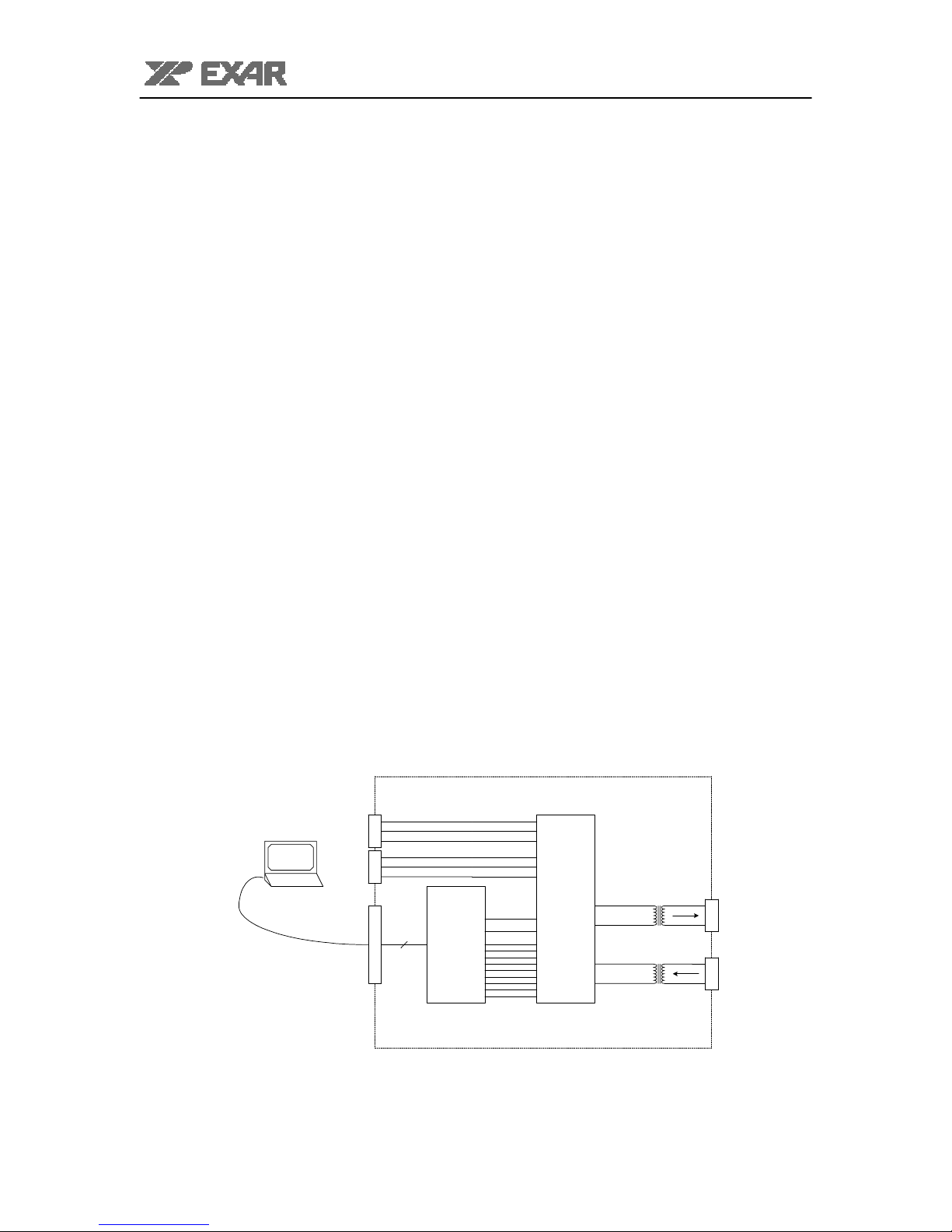
SYSTEM CONFIGURATION-LAB SETUP
The XRT83SL38/L38EVAL application board is setup as a common test c ircuit. Figur e 1 shows a
simplified block diagram of the default test configuration.
PC
Parallel Port Cable
Figure 1 Simplified Block Diagram of the XRT83SL38/L38EVAL Application Board
Page 2 of 23
ConnectorConnector
5
25 DIN Connector
CPLD
A[7:0]
D[7:0]
INT
PCLK
ALE
RST
HW/HOSTB
CS
WR
RD
RDY
TPOS[7:0]
TNEG[7:0]
TCLK[7:0]
RPOS[7:0]
RNEG[7:0]
RCLK[7:0]
XRT83SL38/L38 PCB
XRT83SL38
XRT83L38
LIU
TTIP[7:0]
TRING[7:0]
RTIP[7:0]
RRING[7:0]
ConnectorConnector

XRT83SL38/L38EVAL User Manual
APPLICATION CIRCUITRY
CPLD
The XRT83SL38/L38EVAL uses a CPLD designed to emulate a microproces sor support module
for an 8-Bit parallel interface. Using Exar’s GUI software (included in the evaluation kit), the
XRT83SL38/L38EVAL can be controlled through a standard parallel port cable connected to a
PC. The GUI was written to simplify the evaluation process of Exar’s LIU. Access to all the
control registers and functionality fo all four channels is available. For information on the GUI
software, see the “XRT83SL38/L38EVAL GUI SOFTWARE” s ection of this manual. Figure 2 is a
simplified block diagram of the CPLD interface.
CPLD
A[7:0]
D[7:0]
INT
HW/HOSTB
PCLK
ALE
RST
CS
WR
RD
RDY
XRT83SL38
XRT83L38
LIU
PC
Parallel Port Cable
5
25 DIN Connector
Figure 2 Simplified Block Diagram of the CPLD Interface
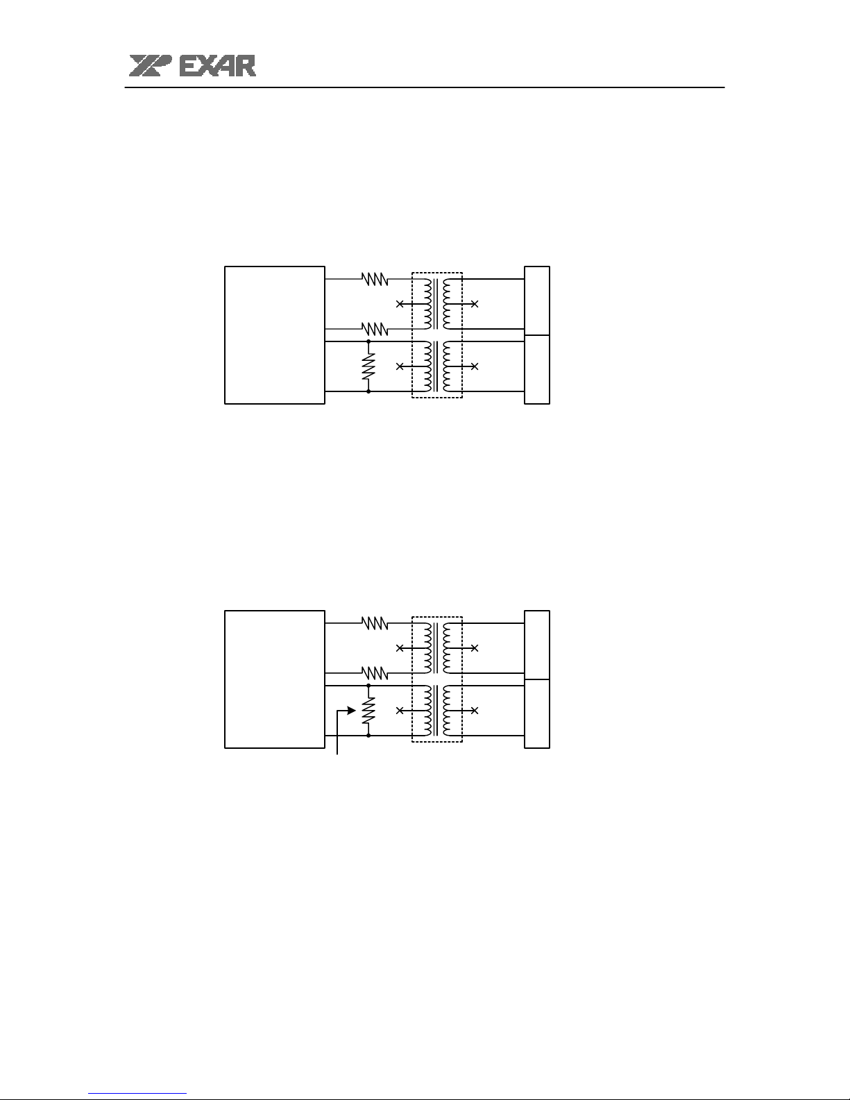
Line Interface Module
Internal Impedance Mode
The XRT83SL38/L38 has an internal and external impedance mode. For internal impedance
mode, no termination resistors are necessary for the transmit outputs. This allows the user to
have one bill of materials for all three applications . Figure 3 is a simplified block diagram of the
internal impedance mode. For external impedance mode, see the following sections for the
resistor values chosen for the corresponding application.
XRT83SL38/L38 LIU
Line Interface Module
TTIP
0.47uF
TRING
RTIP
RRING
Figure 3 Simplified Block Diagram of the Internal Impedance Mode
Page 3 of 23
XRT83SL38/L38EVAL User Manual
External Impedance Mode (T1/J1, 1.544MHz, 100ohm/110ohm)
The XRT83SL38/L38EVAL can be programmed for external impedance mode through the
microprocessor interface. For T1 applications, two 3.1ohm resistors are necessary on the
transmit outputs of the LIU. A 100ohm resistor is necess ary on the rec eiver inputs . (Note: Thes e
values do not change when using either a 1:2 or 1:2.45 turns ratio on the tr ansmit side) Figure 4
is a simplified block diagram of the external mode for T1 applications.
XRT83SL38/L38 LIU
TTIP
TRING
RTIP
Line Interface Module
3.1
3.1
100
1:2
RRING
Figure 4 Simplified Block Diagram of the External Mode, T1/J1
External Impedance Mode (E1, 2.048MHz, 75ohm or 120ohm)
The XRT83SL38/L38EVAL can be programmed for external impedance mode through the
microprocessor interface. For E1 applications, two 9.1ohm resistors are necessary on the
transmit outputs of the LIU. A 75ohm or 120ohm resistor is necessary on the receiver inputs.
(Note: The resistor values on the transmit side change to 6.2ohms when using a 1:2.45 turns
ratio) Figure 5 is a simplified block diagram of the external mode for E1 applications.
XRT83SL38/L38 LIU
TTIP
TRING
RTIP
RRING
75 (for 75ohm Termination)
120 (for 120ohm Termination)
Line Interface Module
9.1
9.1
1:2
1:1
Figure 5 Simplified Block Diagram of the External Mode, E1 75ohm and 120ohm
Page 4 of 23
XRT83SL38/L38EVAL User Manual
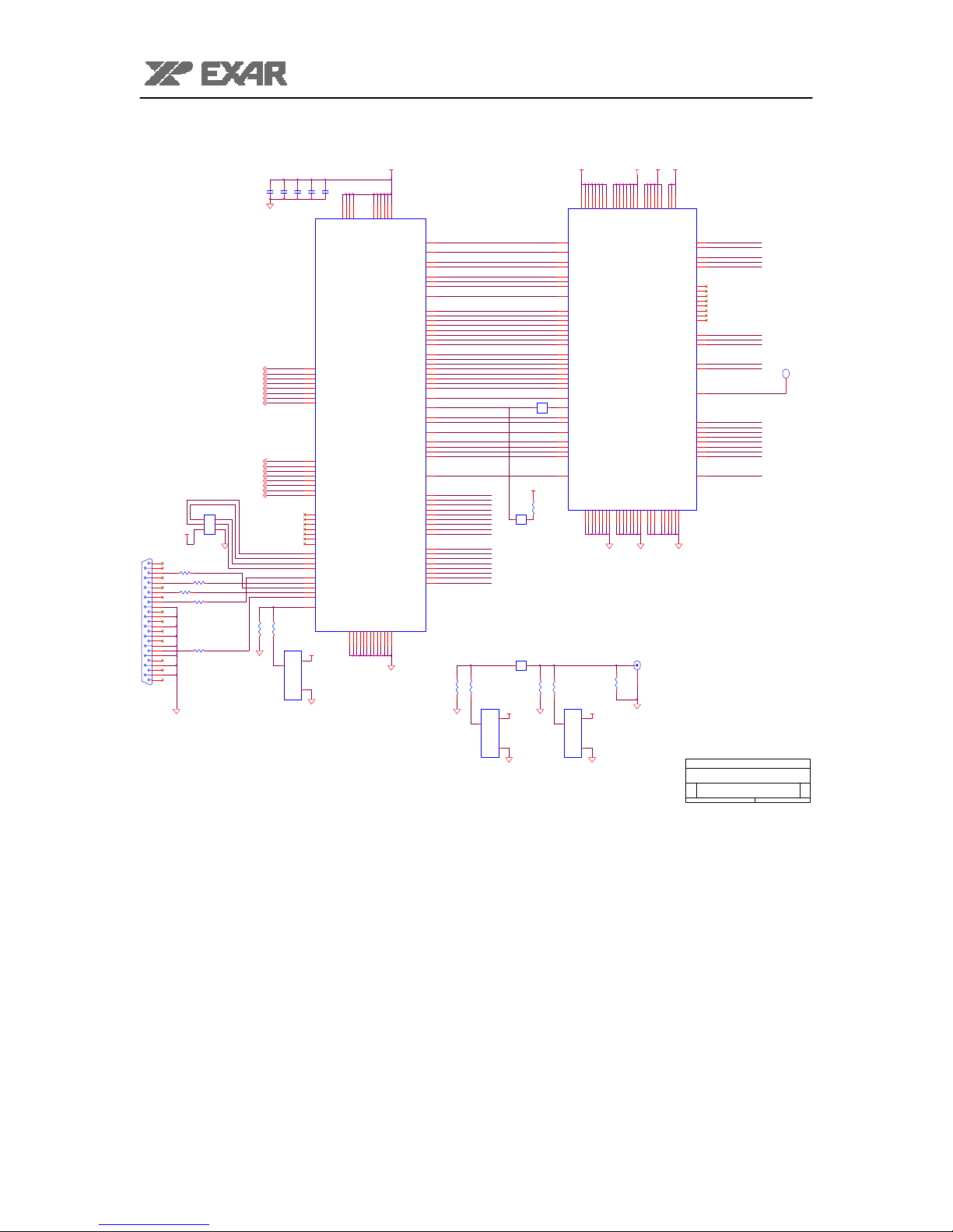
XRT83SL38/L38 OCTAL LONG HAUL, SHORT HAUL LIU MAIN INTERFACE
3V_AVDD
1492183551
TVDD
TVDD
AGND
AGND
AGND
1514739
RVDD
RVDD
RVDD
EXT_VCM
EXT_VCM
R8
OPEN
3V_RVDD
106
122
139
155
RVDD
RVDD
RVDD
RVDD
RVDD
EXT_VCM
EXT_VCM
EXT_VCM
EXT_VCM
EXT_VCM
EXT_VCM
109
119
142
152
EXT CLOCK
SMB1
3V_DVDD
1292425
7879130
181
182
183
AVDD
DVDD
DVDD
DVDD
DVDD
DVDD
DVDD
VDDPLL
AGND
GNDPLL
GNDPLL
13228297677
DGND
DGND
DGND
131
DGND
184
VDDPLL
DGND
185
TERSEL1
TERSEL0
CLKSEL0
CLKSEL1
CLKSEL2
MCLKOUT
186
RxTSEL
TxTSEL
84
TxTSEL
TERSEL1
85
TERSEL0
86
TEST
87
TEST
199
DMO0
10
DMO1
147
DMO2
166
DMO3
62
DMO4
43
DMO5
114
DMO6
95
DMO7
CLKSEL0
187
CLKSEL1
188
CLKSEL2
189
MCLKE1
26
MCLKE1
MCLKT1
27
MCLKT1
23
TAOS7
66
TAOS7
TAOS6
65
TAOS6
TAOS5
64
TAOS5
TAOS4
63
TAOS4
TAOS3
198
TAOS3
TAOS2
197
TAOS2
TAOS1
196
TAOS1
TAOS0
195
TAOS0
ICT
88
ICT
DGND
Design File Name = H:\XRT LIU\XRT83L38\SCHEMATIC\XRT83L38 EVAL.DSN
EXAR AD Infinitum
Title
XRT83SL38/L38
Size Document Number Rev
XRT83SL38/L38 LONG HAUL, SHORT HAUL LIU D
C
Date: Sheet
13Tuesday, September 17, 2002
TP1
T
1
of
P1
DB25
3V_SUP
C4
C5
C2
C3
C1
0.1uF
0.1uF
0.1uF
0.1uF
0.1uF
84284
1411375573
109
VCC
VCC
VCC
VCC
GND
GND
GND
182936476272899099
127
VCCIO
VCCIO
VCCIO
VCCIO
VCCIO
VCCIO
4
SR/DR
126
RESET
41
JASEL1
43
JASEL0
46
FIFOS
121
RxRES0
124
RxRES1
113
RxMUTE
33
A7_LOOP13
31
A6_LOOP03
28
A5_LOOP12
27
A4_LOOP02
26
A3_LOOP11
25
A2_LOOP01
24
A1_LOOP10
23
A0_LOOP00
135
D7_LOOP14
134
D6_LOOP04
133
D5_LOOP15
132
D4_LOOP05
131
D3_LOOP16
130
D2_LOOP06
129
D1_LOOP17
128
D0_LOOP07
106
PCLK_ATAOS
103
INT_TRATIO
101
PTS1_RCLKE
102
PTS2_TCLKE
14
RDY_EQC4
15
CS_EQC3
16
ALE_EQC2
19
WR_EQC0
17
RD_EQC1
125
MODE
RxTSEL
120
RxTSEL
TxTSEL
119
TxTSEL
TERSEL1
118
TERSEL1
TERSEL0
117
TERSEL0
TEST
116
TEST
CLKSEL0
22
CLKSEL0
CLKSEL1
21
CLKSEL1
CLKSEL2
20
CLKSEL2
ICT
115
ICT
TAOS7
136
TAOS7
TAOS6
137
TAOS6
TAOS5
138
TAOS5
TAOS4
139
TAOS4
TAOS3
10
TAOS3
TAOS2
11
TAOS2
TAOS1
12
TAOS1
TAOS0
13
TAOS0
GND
GND
GND
GND
GND
GND
GND
GND
GND
GND
108
114
123
144
R9
4.7k
MCLKT1
R10
36
U4
5
1.544MHz
J2
1 2
++
J3
1 2
++
3V_SUP
8
VCC
CLK
4
GND
U2
TxON7
TxON6
TxON5
TxON4
TxON3
TxON2
TxON1
TxON0
CODES7
CODES6
CODES5
CODES4
CODES3
CODES2
CODES1
CODES0
H1
1
2
+
+
3
4
+
+
5
6
+
+
3V_SUP
JTAG
1
14
R2
2
15
470
R3
3
16
470
R4
4
17
470
R5
5
18
470
6
19
7
20
8
21
9
22
R13
10
23
36
11
24
12
25
13
107
TxON7
110
TxON6
111
TxON5
112
TxON4
34
TxON3
35
TxON2
39
TxON1
40
TxON0
XC95144XL
104
CODES7
105
CODES6
140
CODES5
142
CODES4
45
CODES3
44
CODES2
9
CODES1
7
CODES0
32
GCK2
38
GCK3
5
GTS1
6
GTS2
2
GTS3
3
GTS4
143
GSR
65
TMS
67
TCK
63
TDI
122
TDO
70
SRST
68
SCS
66
SCK
69
SDI
71
SDO
30
MCLK
R7
R6
36
4.7k
U3
3V_SUP
8
VCC
5
CLK
4
GND
16.384MHz
3V_RVDD
U1A
8124145112
116
145
TVDD
TVDD
TVDD
TVDD
TVDD
TVDD
30 83
SR/DR RxTSEL
75
RESET
168
JASEL1
167
JASEL0
134
FIFOS
82
RxRES0
81
RxRES1
89
RxMUTE
173
A7_LOOP13
174
A6_LOOP03
175
A5_LOOP12
176
A4_LOOP02
177
XRT83SL38/L38
A3_LOOP11
178
A2_LOOP01
179
A1_LOOP10
180
A0_LOOP00
67
D7_LOOP14
68
D6_LOOP04
69
D5_LOOP15
70
D4_LOOP05
71
D3_LOOP16
72
D2_LOOP06
73
D1_LOOP17
74
D0_LOOP07
94
PCLK_ATAOS
J1
127
1 2
INT_TRATIO
++
133
PTS1_RCLKE
128
PTS2_TCLKE
194
RDY_EQC4
193
CS_EQC3
192
ALE_EQC2
190
WR_EQC0
191
RD_EQC1
80
MODE
3V_SUP
R1
10k
AGND
AGND
AGND
AGND
AGND
614143
118
1105153848
MCLKE1
R11
R12
4.7k
36
U5
3V_SUP
8
VCC
5
CLK
4
GND
2.048MHz
Figure 6 XRT83SL38/L38EVAL Schematic Page 1
Page 5 of 23
XRT83SL38/L38EVAL User Manual
CODES0
CODES1
CODES2
CODES3
C32
RCLK0
RPOS0
RNEG0
RCLK1
RPOS1
RNEG1
RCLK2
RPOS2
RNEG2
RCLK3
RPOS3
RNEG3
C29
0.1uF
C33
C30
0.1uF
0.1uF
C34
0.1uF
S2
1
2
3
45
HEADER 4X2
S5
1
2
3
45
HEADER 4X2
S7
1
2
3
45
HEADER 4X2
S10
1
2
3
45
HEADER 4X2
0.1uF
C22
C35
8
7
6
8
7
6
8
7
6
8
7
6
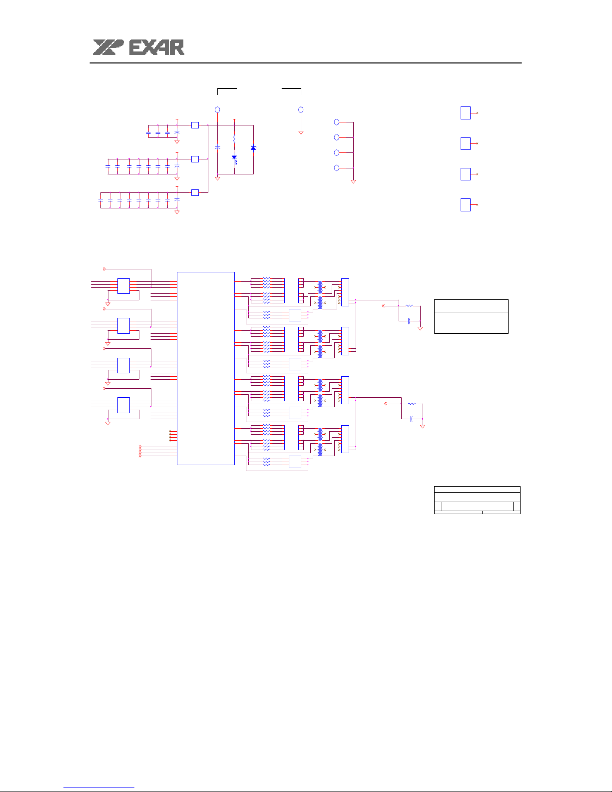
POWER CIRCUITRY
3V_AVDD
C13
C12
C14
C11
0.1uF
0.1uF
0.1uF
3V_DVDD
C25
C24
C26
0.1uF
0.1uF
C23
0.1uF
C36
0.1uF
C16
0.1uF
0.1uF
0.1uF
3V_RVDD
C38
C37
C39
C31
0.1uF
0.1uF
0.1uF
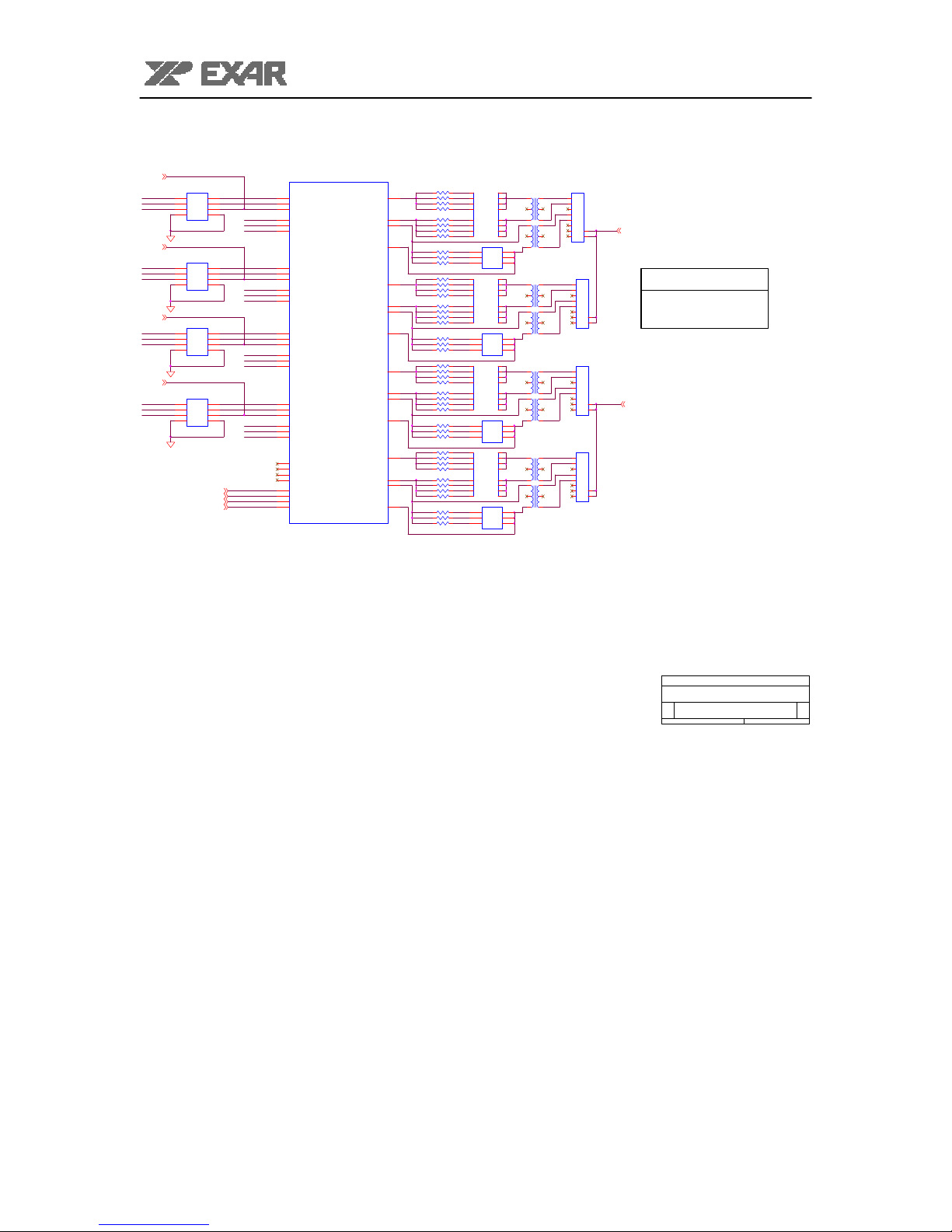
LIU TRANSMIT AND RECEIVE
203
204
205
RCLK0
207
RPOS0
1
RNEG0
208
202
201
200
RCLK1
21
RPOS1
19
RNEG1
20
163
164
165
RCLK2
136
RPOS2
138
RNEG2
137
162
161
160
RCLK3
158
RPOS3
156
RNEG3
157
206
22
135
159
TxON0
TxON1
TxON2
TxON3
169
170
171
172
3V
B1
J4
1 2
++
+
10uF
+
C15
J5
1 2
++
+
10uF
J14
1 2
++
+
10uF
U1B
TCLK0
TPOS0
TNEG0_CODES0
RCLK0
RPOS0
RNEG0_LCV0
TCLK1
TPOS1
TNEG1_CODES1
RCLK1
RPOS1
RNEG1_LCV1
XRT83SL38/L38
TCLK2
TPOS2
TNEG2_CODES2
RCLK2
RPOS2
RNEG2_LCV2
TCLK3
TPOS3
TNEG3_CODES3
RCLK3
RPOS3
RNEG3_LCV3
RLOS0
RLOS1
RLOS2
RLOS3
TxON0
TxON1
TxON2
TxON3
BANNANA PLUGS
1
3V_SUP
470
R14
10uF
D2
LED
9
TRING0
7
TTIP0
4
RRING0
3
RTIP0
11
TRING1
13
TTIP1
16
RRING1
17
RTIP1
146
TRING2
144
TTIP2
141
RRING2
140
RTIP2
148
TRING3
150
TTIP3
153
RRING3
154
RTIP3
D1
5.6V
2 1
R89 0.47uF
R90 3.0
R91 6.2
R92 9.1
R93 0.0
R94 3.0
R95 6.2
R96 9.1
R97 25.0
R98 18.7
R99 30.1
R100 0.47uF
R101 3.0
R102 6.2
R103 9.1
R104 0.0
R105 3.0
R106 6.2
R107 9.1
R108 25.0
R109 18.7
R110 30.1
R111 0.47uF
R112 3.0
R113 6.2
R114 9.1
R115 0.0
R116 3.0
R117 6.2
R118 9.1
R119 25.0
R120 18.7
R121 30.1
R122 0.47uF
R123 3.0
R124 6.2
R125 9.1
R126 0.0
R127 3.0
R128 6.2
R129 9.1
R130 25.0
R131 18.7
R132 30.1
GND
B2
1 2
++
S27
3 4
++
5 6
++
7 8
++
9 10
++
11 12
++
13 14
++
15 16
++
5612
34
1 2
++
3 4
++
5 6
++
7 8
++
9 10
++
11 12
++
13 14
++
15 16
++
5612
34
1 2
++
S31
3 4
++
5 6
++
7 8
++
9 10
++
11 12
++
13 14
++
15 16
++
5612
34
1 2
++
S33
3 4
++
5 6
++
7 8
++
9 10
++
11 12
++
13 14
++
15 16
++
5612
34
1
T1
8
2
S28
See Note 1
T2
8S29
2
S30
See Note 1
T3
8
2
S32
See Note 1
T4
8
2
S34
See Note 1
GROUND POINTS
TP2
1
T
TP3
1
T
TP4
1
T
TP5
1
T
J6
9
1
2
1067
3
4
11
5
143
6
78910
15
161
RJ48
J7
9
1
2
1067
3
4
11
5
143
6
78910
15
161
RJ48
J8
9
1
2
1067
3
4
11
5
143
6
78910
15
161
RJ48
J9
9
1
2
1067
3
4
11
5
143
6
78910
15
161
RJ48
ISOLATION1
ISOLATION2
OPEN
R51
OPEN
OPEN
MOUNTING HOLES
Tx=1:2, Rx=1:1
Note 1: Transformer Selection
C27
TRANSPOWER SMD606-05
+
HALO TG74-1505N1
R88
C28
+
OPEN
M1
MHOLE
M2
MHOLE
M3
MHOLE
M4
MHOLE
1
MH
1
MH
1
MH
1
MH
Figure 7 XRT83SL38/L38EVAL Schematic Page 2
Page 6 of 23
Design File Name = H:\XRT LIU\XRT83L38\SCHEMATIC\XRT83L38 EVAL.DSN
EXAR AD Infinitum
Title
XRT83SL38/L38
Size Document Number Rev
XRT83SL38/L38 LONG HAUL, SHORT HAUL LIU D
C
Date: Sheet
of
23Tuesday, July 02, 2002
XRT83SL38/L38EVAL User Manual
LIU TRANSMIT AND RECEIVE
CODES4
RCLK4
RPOS4
RNEG4
CODES5
RCLK5
RPOS5
RNEG5
CODES6
RCLK6
RPOS6
RNEG6
CODES7
RCLK7
RPOS7
RNEG7
S15
1
8
2
7
3
6
45
HEADER 4X2
S18
1
8
2
7
3
6
45
HEADER 4X2
S20
1
8
2
7
3
6
45
HEADER 4X2
S23
1
8
2
7
3
6
45
HEADER 4X2
TxON4
TxON5
TxON6
TxON7
RCLK4
RPOS4
RNEG4
RCLK5
RPOS5
RNEG5
RCLK6
RPOS6
RNEG6
RCLK7
RPOS7
RNEG7
U1C
58
TCLK4
57
TPOS4
56
TNEG4_CODES4
54
RCLK4
52
RPOS4
53
RNEG4_LCV4
59
TCLK5
60
TPOS5
61
TNEG5_CODES5
32
RCLK5
34
RPOS5
33
RNEG5_LCV5
XRT83SL38/L38
98
TCLK6
97
TPOS6
96
TNEG6_CODES6
125
RCLK6
123
RPOS6
124
RNEG6_LCV6
99
TCLK7
100
TPOS7
101
TNEG7_CODES7
103
RCLK7
105
RPOS7
104
RNEG7_LCV7
55
RLOS4
31
RLOS5
126
RLOS6
102
RLOS7
90
TxON4
91
TxON5
92
TxON6
93
TxON7
TRING4
TTIP4
RRING4
RTIP4
TRING5
TTIP5
RRING5
RTIP5
TRING6
TTIP6
RRING6
RTIP6
TRING7
TTIP7
RRING7
RTIP7
44
46
49
50
42
40
37
36
115
117
120
121
113
111
108
107
R133 0.47uF
R134 3.0
R135 6.2
R136 9.1
R137 0.0
R138 3.0
R139 6.2
R140 9.1
R141 25.0
R142 18.7
R143 30.1
R144 0.47uF
R145 3.0
R146 6.2
R147 9.1
R148 0.0
R149 3.0
R150 6.2
R151 9.1
R152 25.0
R153 18.7
R154 30.1
R155 0.47uF
R156 3.0
R157 6.2
R158 9.1
R159 0.0
R160 3.0
R161 6.2
R162 9.1
R163 25.0
R164 18.7
R165 30.1
R166 0.47uF
R167 3.0
R168 6.2
R169 9.1
R170 0.0
R171 3.0
R172 6.2
R173 9.1
R174 25.0
R175 18.7
R176 30.1
1 2
++
S35
3 4
++
5 6
++
7 8
++
9 10
++
11 12
++
13 14
++
15 16
++
5612
34
1 2
++
S37
3 4
++
5 6
++
7 8
++
9 10
++
11 12
++
13 14
++
15 16
++
5612
34
1 2
++
S39
3 4
++
5 6
++
7 8
++
9 10
++
11 12
++
13 14
++
15 16
++
5612
34
1 2
++
S41
3 4
++
5 6
++
7 8
++
9 10
++
11 12
++
13 14
++
15 16
++
5612
34
T5
J10
9
8
2
S36
See Note 1
8
2
S38
See Note 1
8
2
S40
See Note 1
8
2
S42
See Note 1
1
2
1067
3
4
11
5
143
6
78910
15
161
RJ48
T6
9
1067
11
143
15
161
T7
9
1067
11
143
15
161
T8
9
1067
11
143
15
161
J11
1
2
3
4
5
6
78910
RJ48
J12
1
2
3
4
5
6
78910
RJ48
J13
1
2
3
4
5
6
78910
RJ48
ISOLATION1
Tx=1:2, Rx=1:1
Note 1: Transformer Selection
TRANSPOWER SMD606-05
HALO TG74-1505N1
ISOLATION2
Design File Name = H:\XRT LIU\XRT83L38\SCHEMATIC\XRT83L38 EVAL.DSN
EXAR AD Infinitum
Title
XRT83SL38/L38
Size Document Number Rev
XRT83SL38/L38 LONG HAUL, SHORT HAUL LIU D
C
Date: Sheet
of
33Tuesday, July 02, 2002
Figure 8 XRT83SL38/L38EVAL Schematic Page 3
Page 7 of 23
 Loading...