

Exar XRP6142 User Manual
XXRRPP6611442
R
R
SSyynncchhrroonnoouuss SStteepp--DDoowwnn CCoonnttrroolllleerr wwiitthh DDD
MMeemmoor
ryy TTeerrmmiinnaattiioonn
2
D
July 2010 Rev. 0.0.2
GENERAL DESCRIPTION
EEVVAALLUUAATTIIOONN BBOOAARRDD MMAANNUUAALL
The EXAR XRP6142 Evaluation kit is a fully
assembled and tested surface-mount PCB that
demonstrates the XRP6142 constant on-time
buck controller. The switch-mode power
supply regulator generates a preset 2.5V
output with a load of up to 15A.
The EVB kit requires a single input voltage V
source of 4.5V to 5.5V if V
jumper J1. If V
is supplied through an
CC
is tied to V
CC
IN
IN
via
independent 5V supply then the converter can
operate with V
ranging from 3.3V to 5.5V.
IN
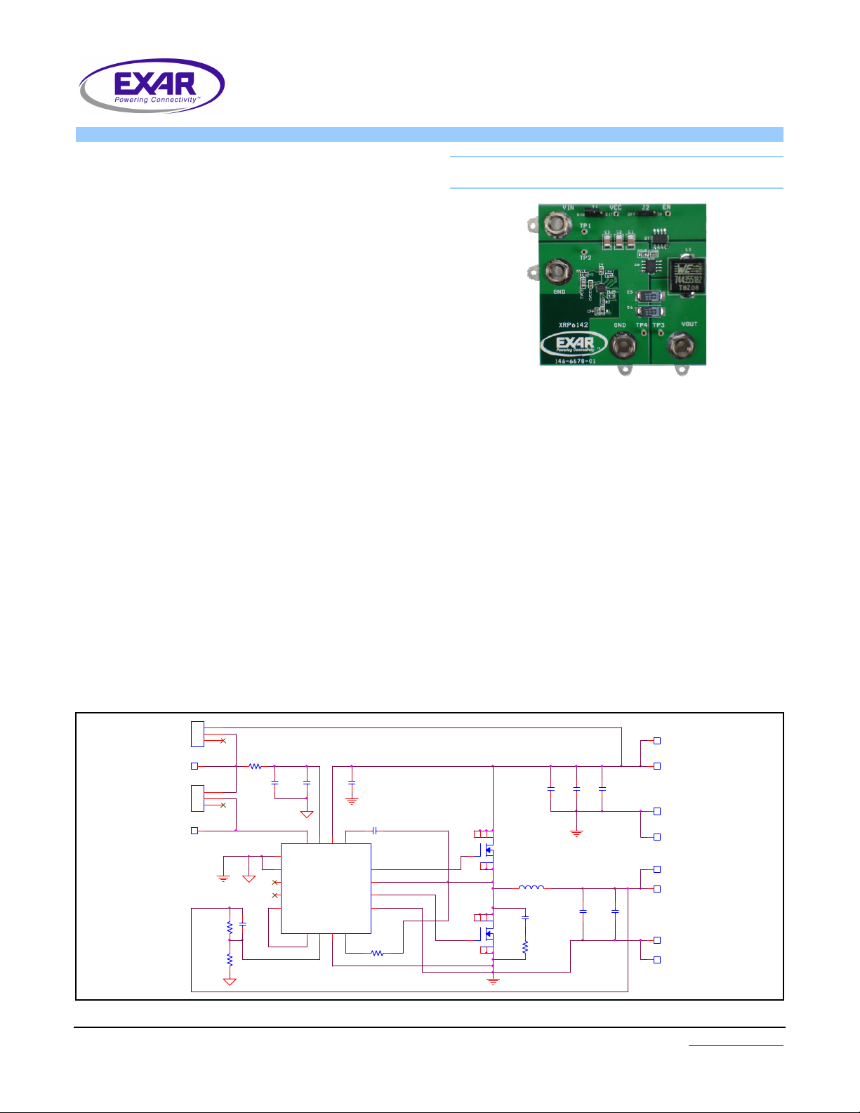
EVALUATION BOARD SCHEMATICS
VIN
1
1
2
2
3
J1
3
VCC
J2
EN
EXT
OFF
1
2
3
ON
38.3k, 1%
10k, 1%
1
2
3
R1
R2
RVC C 10 O hm
CVCC1
CVCC
4.7uF
0
1
2
3
4
CFF
1nF
0.1uF
16
PAD
XRP 6142EL2.0-F
AGND
VTTR EF
VDDQ/2
VREF
15
14
EN
VIN
VCC
U1
REFIN5FB6CSGND7ILIM
C4
0.1uF
CBST 0.1uF
13
BST
GH
SW
GL
PGND
8
RLIM 2.2k
12
11
10
9
FEATURES
• Input Voltage Range of 4.5V – 5.5V
(V
CC=VIN
)
• Input Voltage Range of 3.3V – 5.5V
=5V)
(V
CC
• 15A output current
• Current limit with hiccup
• Internal soft-start
• Internal bootstrap diode
• No compensation required
• Precision Enable
TP1
VIN
C1
47uFC247uFC347uF
876
5
QT
Si4164DY
4
123
L1
1 2
0.82uH
C6
Csnb
3.9nF
Rsnb
0.22 Ohm
C5
220uF
220uF
876
5
QB
Si4164DY
4
123
GND
TP2
TP3
VOUT
GND
TP4
Figure 1: XRP6142 Evaluation Board Schematics
Exar Corporation www.exar.com
48720 Kato Road, Fremont CA 94538, USA Tel. +1 510 668-7000 – Fax. +1 510 668-7001

R
R
PIN ASSIGNEMENT
PIN DESCRIPTION
XXRRPP6611442
SSyynncchhrroonnoouuss SStteepp--DDoowwnn CCoonnttrroolllleerr wwiitthh DDD
MMeemmoor
Figure 2: XRP6142 Pin Assignment
ryy TTeerrmmiinnaattiioonn
2
D
Name Pin Number Description
AGND 1 Analog Ground
VTTREF 2 VTT reference for DDR applications. Buffered output of VDDQ/2
VDDQ/2 3 Voltage used for the input to the VTT buffer
V
4 Precision reference output
REF
REFIN 5 Reference input to the switching-regulator feedback comparator
FB 6 Feedback input to feedback comparator
CSGND 7 Current-sense ground
ILIM 8
PGND 9 Gate driver GND.
GL 10 Low-side N-channel MOSFET driver
SW 11 Switch node for floating-high-side gate drive
GH 12 High-side N-channel MOSFET driver
BST 13 Bootstrap capacitor to drive the high-side gate driver, GH
VIN 14 Input voltage for the power train
Vcc 15
EN 16 Precision enable pin. Pulling this pin above 1.2V will turn the part on
Thermal pad - Internally connected to AGND
Connect a resistor between this pin and the low-side current-sense element in order to
set the current-limit-trip threshold. See applications section for instructions on how to
set this resistor
Input voltage for the XRP6142 internal circuitry and gate drives. Vin and Vcc can be
tied together when Vin ≥ 3.0V
ORDERING INFORMATION
Refer to XRP6142’s datasheet and/or www.exar.com for exact and up to date ordering information.
© 2010 Exar Corporation 2/6 Rev. 0.0.2
 Loading...