

Exar XRP2523 User Manual
XXRRPP22552233
11..55AA SSiinnggllee CChhaannnneell UUSSBB 33..00 PPoowweerr DDiissttrriibbuuttiioonn SSwwiittcchh
October 2012
Rev. 1.0.0
EEVVAALLUUAATTIIOONN BBOOAARRDD MMAANNUUAALL
U1 XRP2523
FLG
3
EN1OUT
5
IN
4
GND
2
VIN = 3.2V - 6.5V
CLB2
DNP
R2
DNP
R4
DNP
R1
10k
CIN1
DNP
GND
CLA1
22uF
CIN2
1uF
ENB
U2 DNP
ENB
4
FLGA
2
ENA1OUTA
8
GND
6
IN
7
OUTB
5
FLGB
3
VOUTB
VLA
CLB1
DNP
VOUTA
VIN
ENA
VLB
R3
DNP
FLGA
CLA2
0.1uF
FLGB
GENERAL DESCRIPTION
The Exar XRP2523 Evaluation board (EVB) is a
full assembled and tested surface-mount PCB
that demonstrates the XRP2523 single-channel
integrated high-side power distribution
switches.
Optimized for USB V
power distribution, the
BUS
XRP2523 is compliant with the latest USB 3.0
specification and can be used in any self or
bus powered USB applications. It is provided
with an enable pin while an error flag is
available to indicate fault conditions.
XRP2523 is offered in a RoHS compliant
“green”/halogen free 5-pin SOT-23 package.
STANDARD CONFIGURATION
The XRP7659EVB evaluation board is
configured to operate under the following
conditions and parameters:
Input voltage range V
Output current/load range: 0 – 1.5A
: 3.2V – 6.5V
IN
FEATURES
1.5A Single Channel Current Switch
1.5A continuous load current
1.6A Over-current Limit
3.2V to 6.5V Input Voltage Range
USB 2.0 and USB 3.0 Compliant
Active High Enable
Soft Start
Channel Fault Flag Indicator
9ms Blanking Time
UVLO, Reverse Current, Short circuit
and Thermal Shutdown Protection
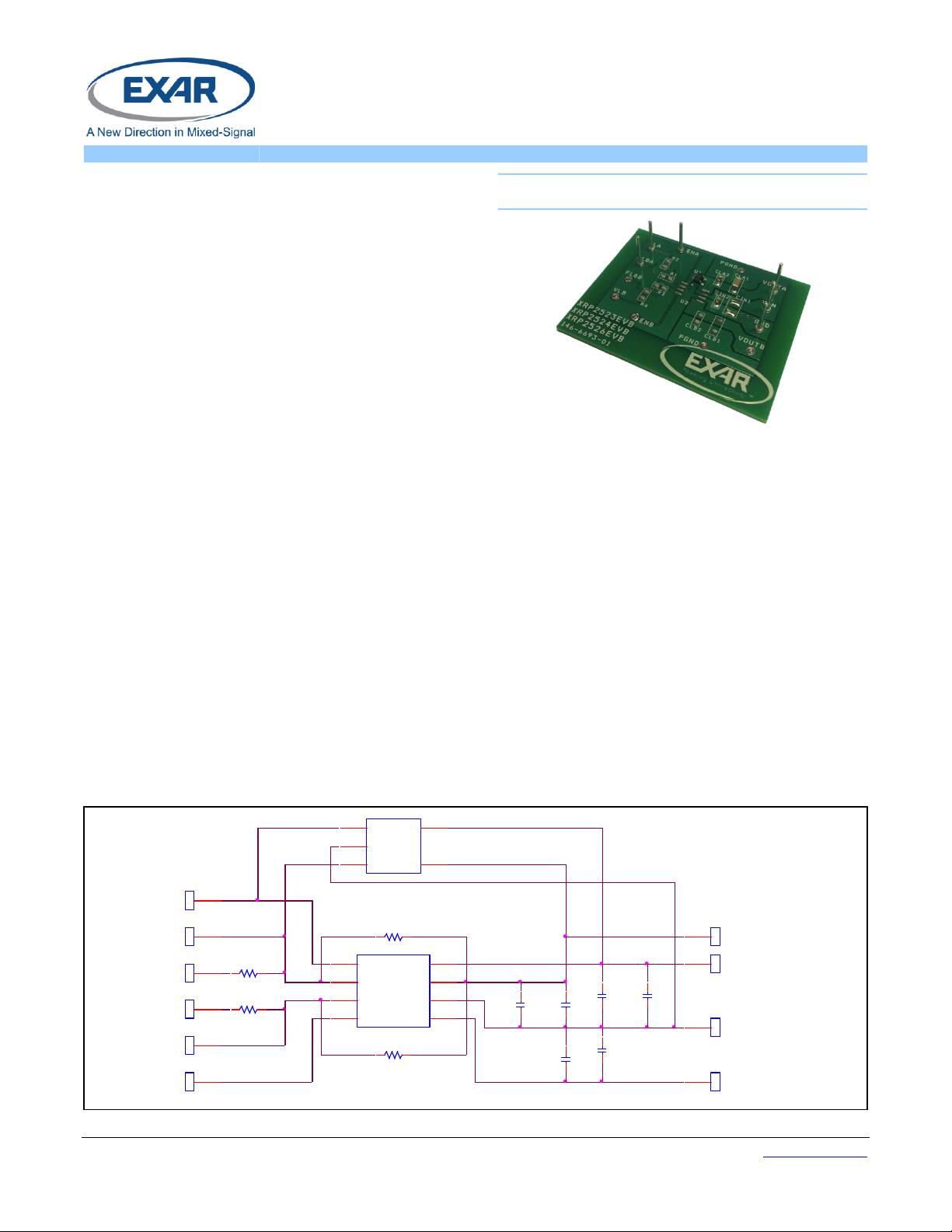
EVALUATION BOARD SCHEMATICS
Exar Corporation www.exar.com
48720 Kato Road, Fremont CA 94538, USA Tel. +1 510 668-7000 – Fax. +1 510 668-7001
Fig. 1: XRP2523 Evaluation Board Schematic
XXRRPP22552233
11..55AA SSiinnggllee CChhaannnneell UUSSBB 33..00 PPoowweerr DDiissttrriibbuuttiioonn SSwwiittcchh
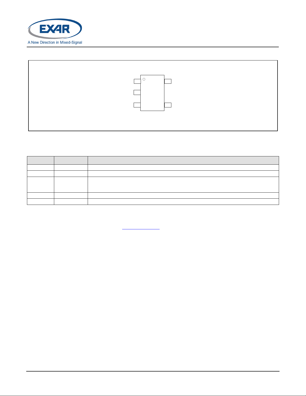
OUT
FLG IN
EN
GND
1
2
3 4
5
XRP2523
SOT-23-5
Name
Pin Number
Description
EN
1
Channel Enable Input
GND
2
Ground Signal
FLG
3
Error Flag Signal
Active low open drain output. Active on over-current, over-temperature, short-circuit or UVLO
conditions.
IN
4
Voltage Input Pin
OUT
5
Voltage Output Pin
PIN ASSIGNMENT
PIN DESCRIPTION – XRP2523
Fig. 2: XRP2523 Pin Assignment
ORDERING INFORMATION
Refer to XRP2523’s datasheet and/or www.exar.com for exact and up to date ordering information.
© 2012 Exar Corporation 2/8 Rev. 1.0.0
XXRRPP22552233
11..55AA SSiinnggllee CChhaannnneell UUSSBB 33..00 PPoowweerr DDiissttrriibbuuttiioonn SSwwiittcchh
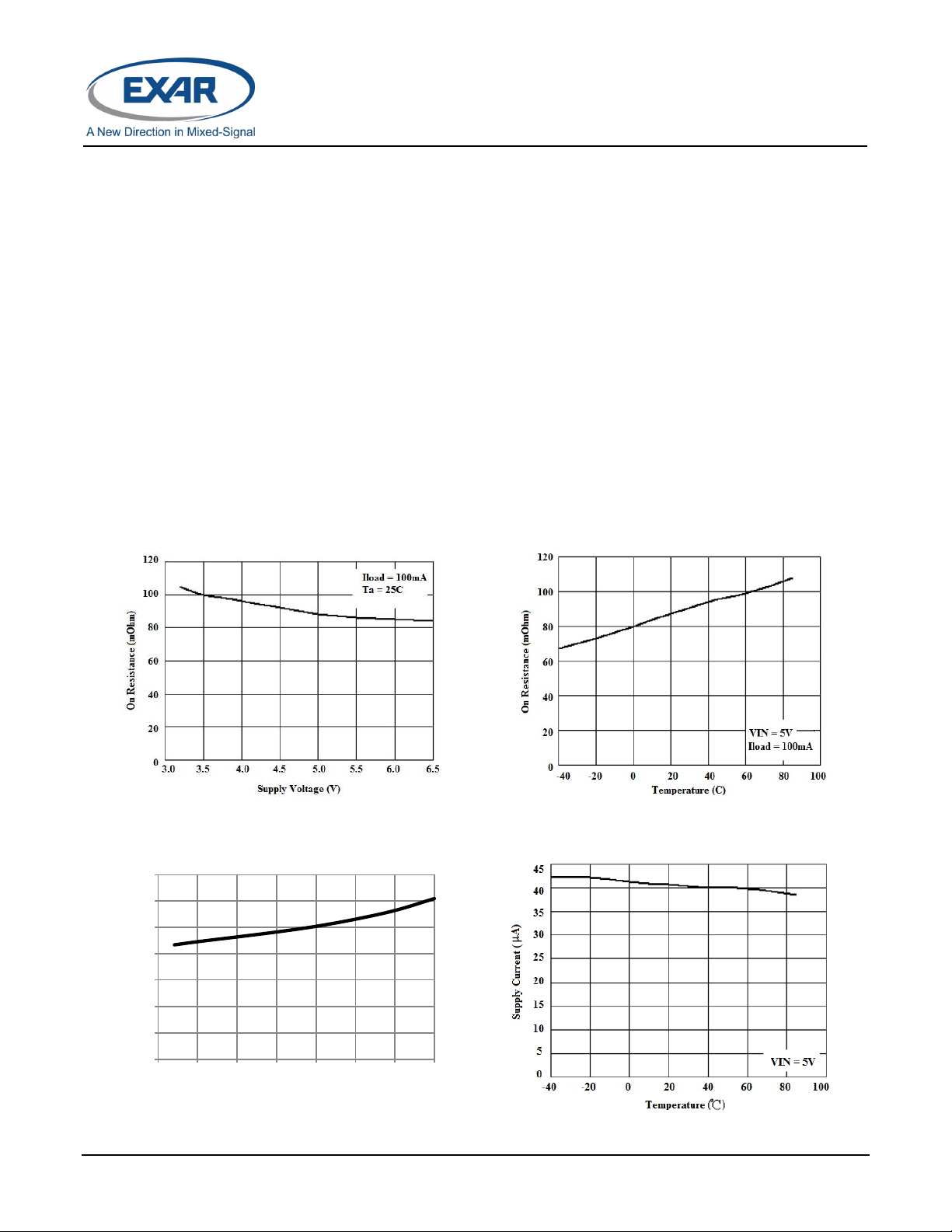
Fig. 3: Output On-Resistance vs. Supply Voltage
Fig. 4: Output On-Resistance vs. Temperature
Fig. 5: ON-State Supply Current vs. Supply Voltage
Fig. 6: ON-State Supply Current vs. Temperature
0
10
20
30
40
50
60
70
3 3.5 4 4.5 5 5.5 6 6.5
On-State Supply Current (µA)
Supply Voltage (V)
Ta = 25°C
USING THE EVALUATION BOARD
Note: The XRP2523 evaluation board is
common with Exar’s XRP2524 and XRP2526
evaluation boards.
PGND connectors on the right hand side of the
board.
Flag pin is pulled up to VIN through a 10kΩ
resistor (provided by default on the board) or
can be instead connected to a separate
INITIAL SETUP
The Board is supplied from EXAR with the
XRP2523 device. Set the input supply to a
voltage between 3.2V to 6.5V and connect it
to VIN and GND connectors on the right side
of the evaluation board.
external power supply voltage VLA.
The board will power-up upon turning on the
input supply and reach the desired output
voltage. The board can operate with a load
current I
Enable pin must be pulled up HIGH to enable
the IC. Connect the load to the VOUT and
TYPICAL PERFORMANCE CHARACTERISTICS
All data taken at VIN = 5V, CIN = 1µF, C
from Application Information section of this datasheet.
= 22µF//0.1µF, TJ = TA = 25°C, unless otherwise specified - Schematic and BOM
OUT
of up to 1.5A.
OUT
© 2012 Exar Corporation 3/8 Rev. 1.0.0
 Loading...