

EXAR XRP1620 Service Manual
XXRRPP7766220
0
June 2009 Rev. 1.0.0
GENERAL DESCRIPTION
The XRP7620 is a multi purpose 4-channel
independently adjustable current sink driver.
Optimized for LED backlighting and
RGBW/RGBA color mixing applications, the
XRP7620 can also be used as a generic
software programmable current sink I/O
expander.
Supporting an industry standard 2-wire I
serial interface, the XRP7620 provides full
independent control of each channel and can
be programmed up to a current of 31.5mA in
steps of 0.5mA. Uniform display brightness is
ensured through better than 3% channel to
channel current matching.
Five internal registers are provided to set
operational configuration and individual
channel current programmation. A specific
shutdown mode allows the device to retain the
previously loaded configuration – operational
and current programming – in order to be
reused upon the next enabling.
The XRP7620 is designed to operate from a
single cell lithium-ion battery or fixed 3.3V or
5.0V power rails and is available in a RoHS
compliant, “green”/halogen free space saving
44--CChhaannnneell AAddjjuussttaabbllee CCuurrrreenntt II22CC CCoonnttrroolllleedd LLEEDD DDrri
APPLICATIONS
• LCD Display & Keypad Backlighting
• Color Coded Indicator Lighting
• RGBW/RGBA Color Mixing
• Cell Phones & Handheld Devices
• Generic Current Sink I/O Expander
2
C
FEATURES
• 4-Channel LED Current Sink Driver
• Individual Channel Current Control
− Up to 31.5mA per channel / 0.5mA Steps
− 100mV Channel Dropout Voltage
2
C Serial Interface
• I
• 2.7V - 5.5V Input Voltage Range
• 3% Channel Current Matching
• Register Retention in Shutdown
• Shutdown Current <1µA
• Thermal and UVLO Built-in Protection
• RoHS Compliant, “Green”/Halogen
Free 2x3mm 8-Pin DFN package
ivveerr
8-pin 2mmx3mm DFN package.
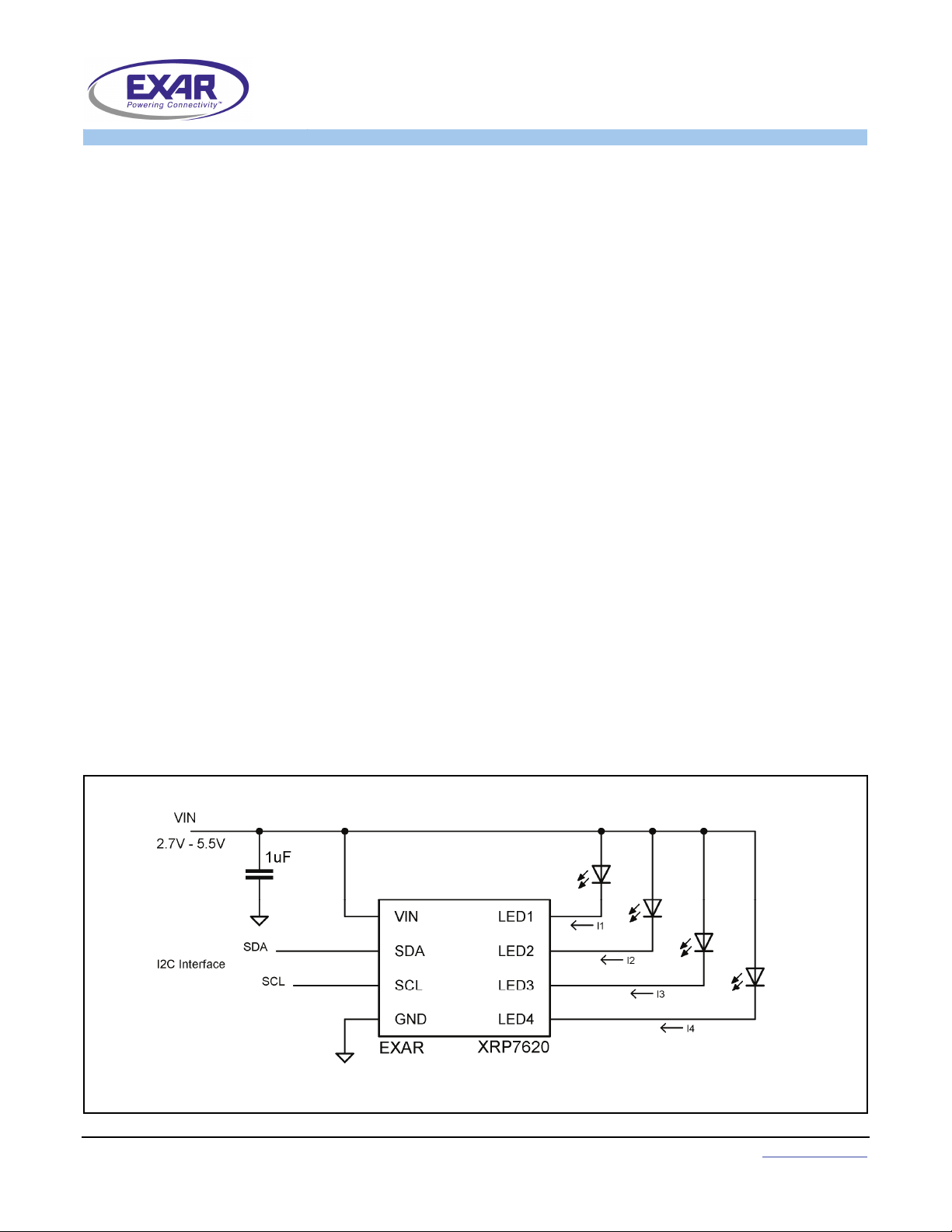
TYPICAL APPLICATION DIAGRAM
Fig. 1: XRP7620 Application Diagram
Exar Corporation www.exar.com
48720 Kato Road, Fremont CA 94538, USA Tel. +1 510 668-7000 – Fax. +1 510 668-7001
XXRRPP7766220
0
44--CChhaannnneell AAddjjuussttaabbllee CCuurrrreenntt II22CC CCoonnttrroolllleedd LLEEDD DDrri
ivveerr
ABSOLUTE MAXIMUM RATINGS
These are stress ratings only and functional operation of
the device at these ratings or any other above those
indicated in the operation sections of the specifications
below is not implied. Exposure to absolute maximum
rating conditions for extended periods of time may affect
OPERATING RATINGS
Input Voltage Range VIN...............................2.7V to 5.5V
Junction Temperature Range ....................-40°C to 100°C
Thermal Resistance θ
...................................... 59°C/W
JA
reliability.
V
, SDA, SCL, LEDx .................................. -0.3V to 6.0V
IN
Storage Temperature .............................. -65°C to 150°C
Power Dissipation ................... Internally Limited (Note 1)
Lead Temperature (Soldering, 10 sec) ................... 300°C
ESD Rating (Human Body Model) ............................. 2kV
ELECTRICAL SPECIFICATIONS
Specifications with standard type are for an Operating Junction Temperature of TJ = 25°C only; limits applying over the full
Operating Junction Temperature range are denoted by a “•”. Minimum and Maximum limits are guaranteed through test,
design, or statistical correlation. Typical values represent the most likely parametric norm at T
reference purposes only. Unless otherwise indicated, V
= 2.7V to 4.6V, CIN = 1µF, TA= –40°C to 85°C, TJ = –40°C to
IN
100°C.
Parameter Min. Typ. Max. Units Conditions
Operating Input Voltage Range 2.7 5.5 V •
Operating Input Current
DAC=000000
Operating Input Current 450 600 µA • I
LED Current accuracy
(includes Line Regulation)
LED Current Matching -3 3 % •
Line Regulation 1 %/V •
30 50 µA • I
-0.3 0.3 mA •
-5 5 %
-8 8 % •
=0, VIN=4.2V
LEDX
LED1=ILED2=ILED3=ILED4
V
= 0.2V to 2.7V
LED
I
≤ 6mA
LEDX
V
= 0.2V to 2.7V
LED
I
> 6mA
LEDX
For same DAC setting
= 0.2V to 2.7V, Note 2
V
LED
Measured as ΔI
V
= 0.2V to 2.7V, Note 3
LED
Current DAC Resolution 6 Bit
Current for DAC=000000 2 µA • Applies to all LEDs
Current for DAC=000001 0.35 0.50 0.65 mA Applies to all LEDs
Maximum LED Current
DAC=111111
30.50 31.75 33.00 mA Applies to all LEDs
For changes between any DAC code
2 µs •
000001 and higher. Current must change
within this time after the last bit of LED
data. V
Maximum Current Change
Settling Time
60 150 µs
Applies to changes between DAC code
000000 and higher or change from 0 to 1
for STATUS bits B5-B2 (channel enable).
Current must change within this time
after the last bit of LED data. V
5.5V
I
=20mA;
LED
Current Source Dropout Voltage 0.1 0.15 V •
The voltage where LED current decreases
3% from nominal value at V
=2.7 to 5.5V
V
IN
Shutdown Supply Current 0.01 1 µA VIN=4.2V
Shutdown Supply Current 5 µA VIN=4.2V, TA=85°C
Thermal Shutdown Die
Temperature
125 150 175 °C Regulator turns off
= 25°C, and are provided for
J
=10mA, VIN=4.2V
OUT /IOUT_AVG
=2.7 to 5.5V
IN
/ΔV
LED
= 1V.
=2.7 to
IN
© 2009 Exar Corporation 2/11 Rev. 1.0.0
XXRRPP7766220
0
44--CChhaannnneell AAddjjuussttaabbllee CCuurrrreenntt II22CC CCoonnttrroolllleedd LLEEDD DDrri
Parameter Min. Typ. Max. Units Conditions
Thermal Shutdown Hysteresis 15 °C Regulator turns on
SDA, SCL Input Logic Low
Voltage
SDA, SCL Input Logic High
Voltage
0.4 V •
1.6 V •
SDA, SCL Timeout for Shutdown 90 150 ms
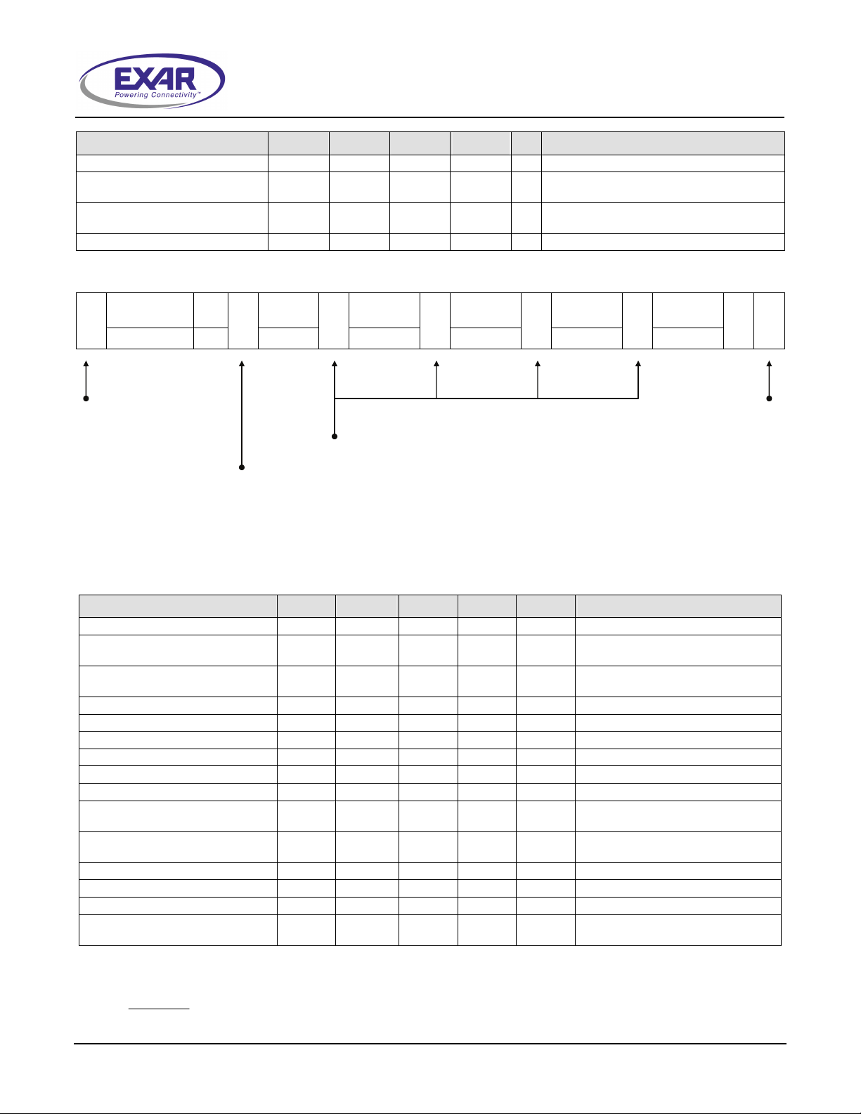
I2C SPECIFICATION
XRP7620
Address
S
7-bit 1/0 A 8-bit
Start Condition
R/W
Status
Data
Acknowledgement
sent by the slave
LED1 Data LED2 Data LED3 Data LED4 Data
A
8-bit
A
8-bit
A
A
8-bit
Acknowledgement
- sent by the slave when R/W=0
- sent by master when R/W=1
Fig. 2: Data Input Format
ivveerr
A SP
8-bit
Stop Condition
I2C TIMING CHARACTERISTICS
Unless otherwise indicated, VIN = 2.7V to 4.6V, CIN = 1µF, TA= –40°C to 85°C, TJ = –40°C to 100°C.
Parameter Symbol Min. Typ. Max. Units Conditions
Serial Clock Frequency f
Bus Free Time between a STOP
and a START
Hold Time, Repeated START
Condition
STOP Condition Setup Time t
Data Hold Time t
Input Data Hold Time t
Data Setup Time t
SCL Clock Low Period t
SCL Clock High Period t
Rise Time of Both SDA and SCL
Signals, receiving
Fall Time of Both SDA and SCL
Signals, Receiving
Fall Time of SDA Transmitting t
Pulse Width of Spike Suppressed tSP 0 50 ns Note 7
Capacitive Load for each Bus Line Cb 400 pF Note 4
I2C Startup Time after UVLO
clears
Note 1: All parameters tested at TA=25 °C. Specifications over temperature are guaranteed by design.
Note 2: LED current matching is calculated by this equation:
400 KHz
SCL
t
1.3 µs
BUF
t
0.6 µs
HD_STA
0.6 ms
SU,STO
HD,DAT(OUT)
HD, DAT(IN)
225 900 ns
0 900 ns
100 ns
SU, DAT
1.3 ms
LOW
0.6 ms
HIGH
t
20+0.1Cb 300 ns Note 4,5
R
t
20+0.1Cb 300 ns Note 4,5
F
20+0.1Cb 250 ns Note 4,5, 6
F.TX
t
1 µs Note 4
SRT
II
−
AVGLED
I
AVG
Where I
%100×
is the average current of 4 channels.
AVG
© 2009 Exar Corporation 3/11 Rev. 1.0.0
XXRRPP7766220
0
Note 3: Ling regulation is calculated by this equation:
−VIII
1
12
×
Δ
AVG
Note 4: Guaranteed by design.
Note 5: Cb = total capacitance of one bus line in pF. t
Note 6: I
Note 7: Input filters on the SDA and SCL inputs suppress noise spikes less than 50ns.
≤6mA. Cb =total capacitance of one bus line in pF. tR and tF measured between 0.3 x VDD and 0.7 VDD.
SINK
Where I1 and I2 is the current at different VIN.
%100
×
44--CChhaannnneell AAddjjuussttaabbllee CCuurrrreenntt II22CC CCoonnttrroolllleedd LLEEDD DDrri
and tF measured between 0.3 x VDD and 0.7 x VDD.
R
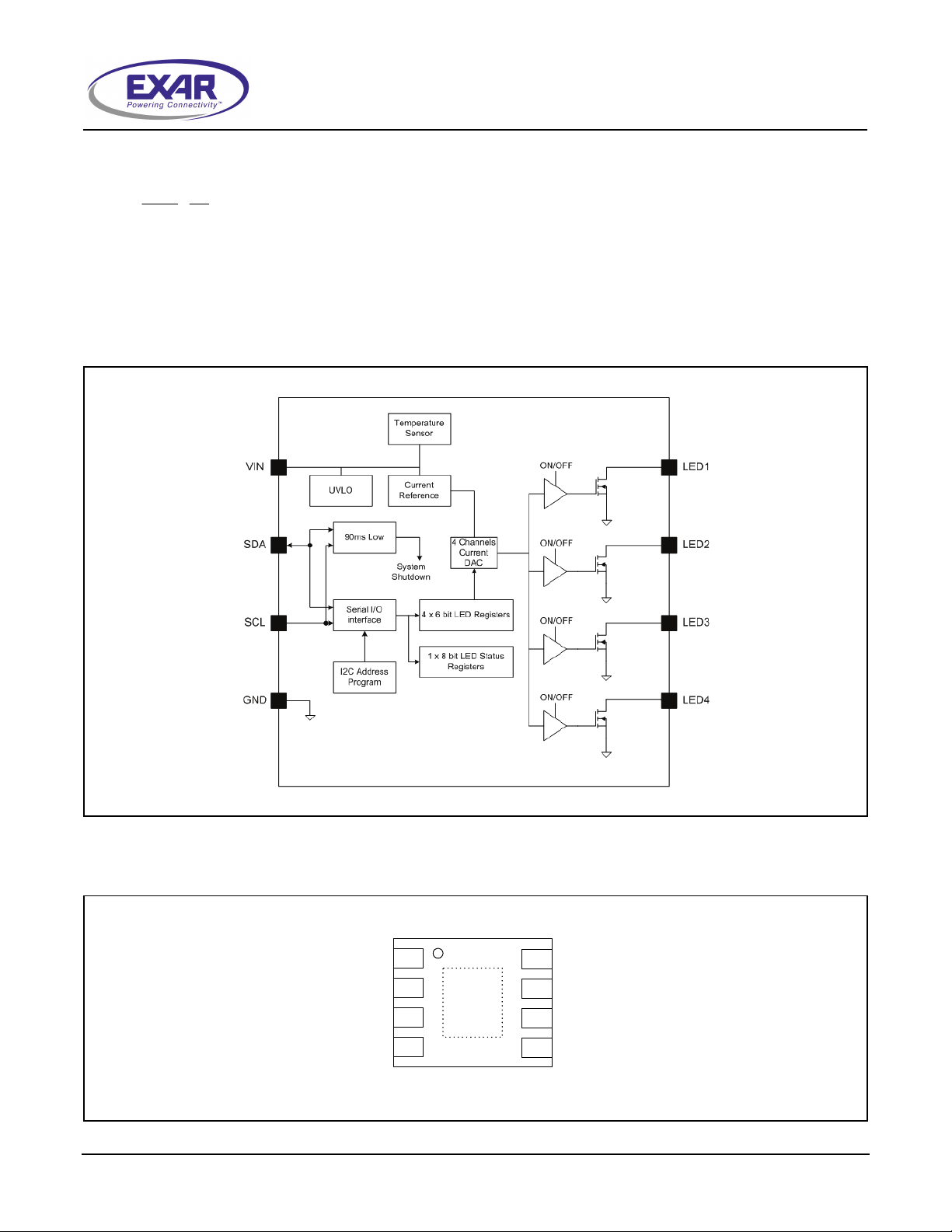
BLOCK DIAGRAM
ivveerr
Fig. 3: XRP7620 Block Diagram
PIN ASSIGNEMENT
2mm x 3mm
VIN
SDA
SCL
GND
1
2
3
4
DFN-8L
Fig. 4: XRP7620 Pin Assignement
© 2009 Exar Corporation 4/11 Rev. 1.0.0
8
LED1
7
LED2
6
LED3
5
LED4
 Loading...