

Exar XR22414-EVB User Manual
XR22414-EVB
U
S
B
QFN
48
PWR
DS Port
1
DS Port
2
DS Port
3
DS Port
4
U2
P
T
C
JUMP
C
M
LED
CAP
JUMP
LED
J8
J8: 1-2 Self Power
2-3 Bus Po wer
LQFP
48
1
24
48
12
U1
LED
P
T
C
JUMP
C
M
LED
CAP
LED
P
T
C
JUMP
C
M
LED
CAP
LED
P
T
C
JUMP
C
M
LED
CAP
LED
Evaluation Board User’s Manual
Introduction
The XR22414 evaluation board is for the Exar USB 2.0 4-Port hub in both the 48 pin LQFP and 48 pin QFN packages. This
manual is intended to guide users to use various functions and configurations of the hub device. Either the 48 pin LQFP
package or 48 pin QFN package EVB can be ordered as shown in Table 1.
Table 1: Ordering Information
Device Ordering Part Number Evaluation Board Ordering Part Number Device Package Device Location
XR22414CV48-F XR22414CV48EVB LQFP 48 U1
XR22414CL48-F XR22414CL48EVB QFN 48 U2
Board Layout and Outline
Evaluation Board outline
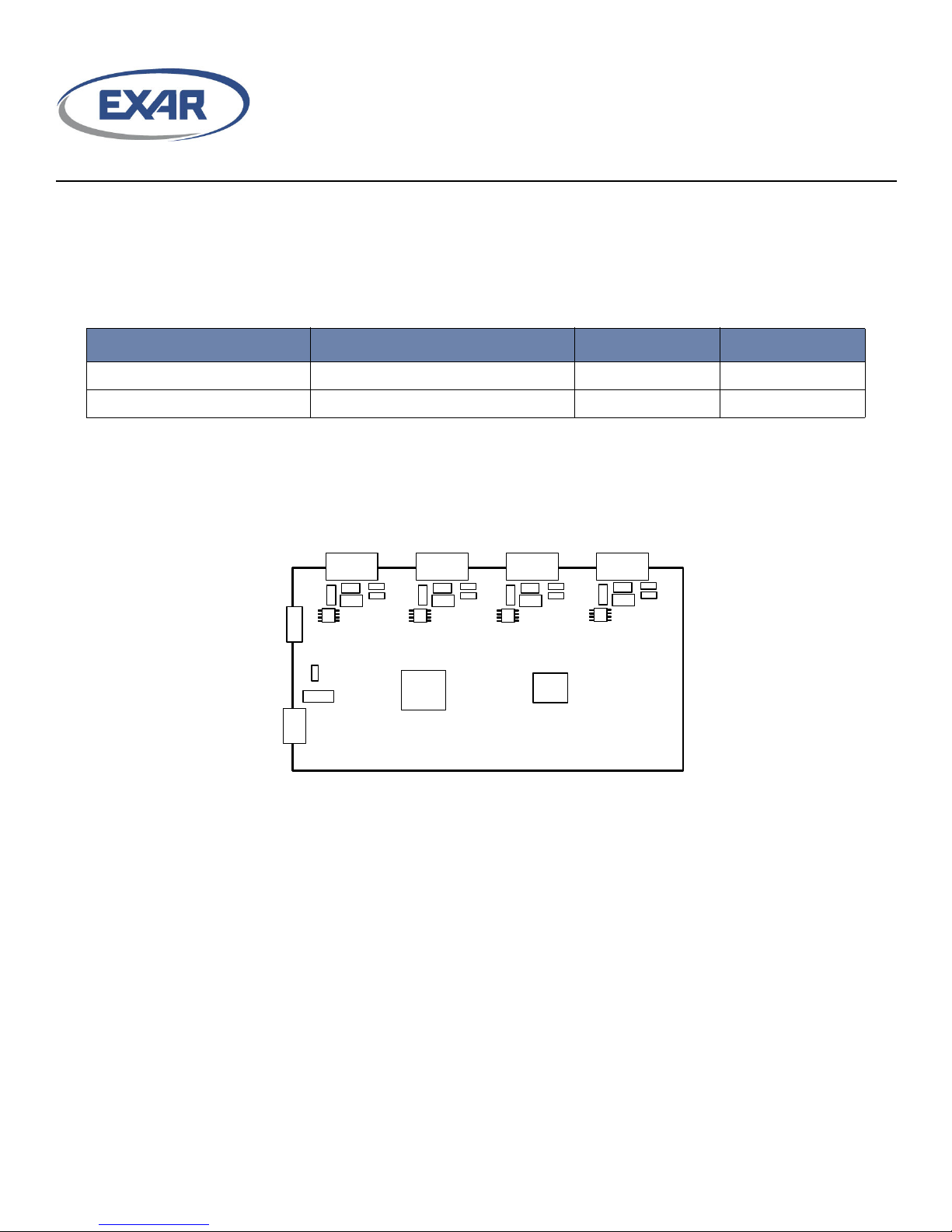
Figure 1 shows the topography of the evaluation board. Either U1 or U2 will be installed depending upon the version of the
evaluation board.
© 2017 Exar Corporation
Figure 1: XR22414 PCB Outline
1 / 8
www.exar.com\XR22414
Rev 1A
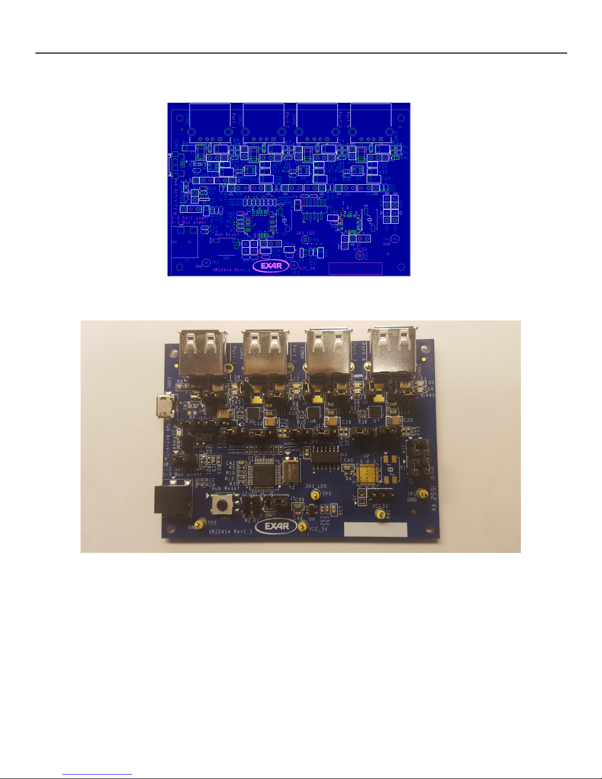
Evaluation Board Layout
Evaluation Board Picture
XR22414 EVB User’s Manual
Hardware Configuration
This section describes the default board settings, when shipped from the factory, and jumper settings that may be used to
reconfigure operation.
Differences between XR22414CV48EVB and XR22414CL48EVB
The XR22414 is available in two packages, a 48 pin LQFP and a 48 pin QFN. The two versions of the evaluation board use
the same bare PCB, but with different components assembled, which includes either the LQFP or QFN package. In order to
avoid trace stubs on high speed USB (480 MHz) nets, 0 ohm resistors are installed from the upstream and all four down-
© 2017 Exar Corporation
Figure 2: XR22414 PCB
2 / 8 www.exar.com\XR22414
Rev 1A

XR22414 EVB User’s Manual
stream USB ports to connect to the QFN48 device for the XR22414CL48EVB. These resistors are not installed for the
LQFP48 EVB.
Power Configurations
The XR22414 EVB may operate in either bus powered or self-powered modes. The power mode must be selected by
jumper J8. If self-powered, the device uses the 5V supplied by the external 5V DC input to J8 power jack. When bus powered, the XR22414 may not be capable of providing sufficient power to all downstream ports. By USB specification, in bus
powered mode, each downstream port may draw 100 mA maximum and the hub itself may draw an additional 100 mA. In
self-powered mode, external 5V must be supplied to the PCB via the J7 power connector and each downstream port may
draw up to 500 mA.
The XR22414 EVB may alternately operate from a 3.3V input. To power the device from 3.3V the REG_EN# pin must be
deasserted and the VCC5 pin must not be connected to a 5V source. The 3.3V power input to should be provided to all
VCC33 pins and the 3V3_OUT pin will not provide an output voltage.
The XR22414 EVB can be configured for either individual or global power monitoring and ganged power control. In individual mode, each port is monitored by an XRP2527 power monitor circuit. In global mode, all four downstream ports power is
combined and monitored by a single monitor circuit. Alternately, power to the downstream ports of the XR22414 EVB can
be monitored by a resettable PTC fuse, or by both the fuse and the power monitor devices. Over-current conditions detected
by either XRP2527 current monitors or PTC fuses are signaled to the OVC# pin of the device, and power out pins (PWR#)
are deasserted to then power down downstream ports.
Table 2 defines the jumper settings on the XR22414 EVB, and the default settings of each jumper when shipped from the
factory.
Table 2: Jumper Settings and components for PCB Power
Jumper Description Default
J8 J8 must be installed either pin 1 to 2 when the XR22414 is self-powered
or pin 2 to 3 when the device is bus powered.
J6 J6 can be used to bypass the inrush current limiting circuit when the
XR22414 is bus powered.
J1, J2, J3, J4, J5 To power the device from 3.3V instead of 5V, the top surface trace
J21, J22, J23, J24,
J25, J26, J27
J9, J10, J15, J16 J9, J10, J15 and J16 are used to select whether the PTC fuse only or
across jumper J3 must be cut disabling the 5V to 3.3V internal regulator.
For the XR22414CV48EVB the top surface trace across jumper J2 must
also be cut and J1 must be installed from pin 2 to 3 to use the external
3.3V LDO voltage. For the XR22414CL48EVB J5 trace must be cut and
J4 must be installed pin 2 to 3.
J21 is used to select global over current monitoring for downstream port
over-current protection. When J21 is installed, global over-current monitoring is selected. When J21 is not installed, individual port over-current
monitoring is selected. If J21 is installed, J25, J26 and J27 should also
be installed to connect port power for all downstream ports together and
J22, J23, and J24 should also be installed to connect unused OVCn#
pins to ground.
current monitor (XRP2527) device is used for downstream port over-current protection.
By default J8 is installed pin 1 to 2
By default J6 is not installed
J2, J3 and J5 are normally not installed.
By Default, J1 in installed pin 1 to 2 for
the XR22414CV48EVB or J4 is installed
pin 1 to 2 for the XR22414CL48EVB.
By default J21, J22, J23, J24, J25, J26
and J27 are not installed.
By default J9, J10, J15 and J16 are
installed from pin 1 to 2.
J11, J12, J17, J18 If J9, J10, J15 and J16 are installed pin 1 to 2, J11, J12, J17 and J18
select whether XRP2527 over-current monitor only or PTC fuse and current monitor devices protect downstream ports.
© 2017 Exar Corporation
By default J11, J12, J17 and J18 are
installed from pin 2 to 3.
3 / 8 www.exar.com\XR22414
Rev 1A
 Loading...