

EXAR XR21V1410 Service Manual

XR21V1410
1-CH FULL-SPEED USB UART
JUNE 2009 REV. 1.0.0
GENERAL DESCRIPTION
The XR21V1410 (V1410) is an enhanced Universal
Asynchronous Receiver and Transmitter (UART) with
a USB interface. The USB interface is fully compliant
to Full Speed USB 2.0 specification that supports 12
Mbps USB data transfer rate. The USB interface also
supports USB suspend, resume and remote wakeup
operations.
The V1410 operates from an internal 48MHz clock
therefore no external crystal/oscillator is required like
previous generation UARTs. With the fractional baud
rate generator, any baud rate can accurately be
generated using the internal 48MHz clock.
The large 128-byte FIFO and 384-byte RX FIFO of
the V1410 helps to optimize the overall data
throughput for various applications. The Automatic
Transceiver Direction control feature simplifies both
the hardware and software for half-duplex RS-485
applications. If required, the multidrop (9-bit) mode
with automatic half-duplex transceiver control feature
further simplifies typical multidrop RS-485
applications.
The V1410 operates from a single 2.97 to 3.63 volt
power supply and has 5V tolerant inputs. The V1410
is available in a 16-pin QFN package.
Software drivers for Windows 2000, XP, Vista, and
CE, as well as Linux and Mac are supported for the
XR21V1410.
FEATURES
• USB 2.0 Compliant Interface
■ Supports 12 Mbps USB full-speed data rate
■ Supports USB suspend, resume and remote
wakeup operations
• Enhanced UART Features
■ Data rates up to 12 Mbps
■ Fractional Baud Rate Generator
■ 128 byte TX FIFO
■ 384 byte RX FIFO
■ 7, 8 or 9 data bits, 1 or 2 stop bits
■ Automatic Hardware (RTS/CTS or DTR/DSR)
Flow Control
■ Automatic Software (Xon/Xoff) Flow Control
■ Multidrop mode w/ Auto Half-Duplex
Transceiver Control
■ Multidrop mode w/ Auto TX Enable
■ Half-Duplex mode
■ Sleep Mode with Remote Wake-up
■ Selectable GPIO or Modem I/O
• Internal 48 MHz clock
• Single 2.97-3.63V power supply
• 5V tolerant inputs
• 16-pin QFN package
APPLICATIONS
• Portable Appliances
• External Converters (dongles)
• Battery-Operated Devices
• Cellular Data Devices
• Factory Automation and Process Controls
• Industrial applications
• Virtual COM Port drivers
■ Windows 2000, XP and Vista
■ Windows CE 4.2, 5.0, 6.0
■ Linux
■ Mac
Exar Corporation 48720 Kato Road, Fremont CA, 94538 • (510) 668-7000 • FAX (510) 668-7017 • www.exar.com
XR21V1410
1-CH FULL-SPEED USB UART REV. 1.0.0
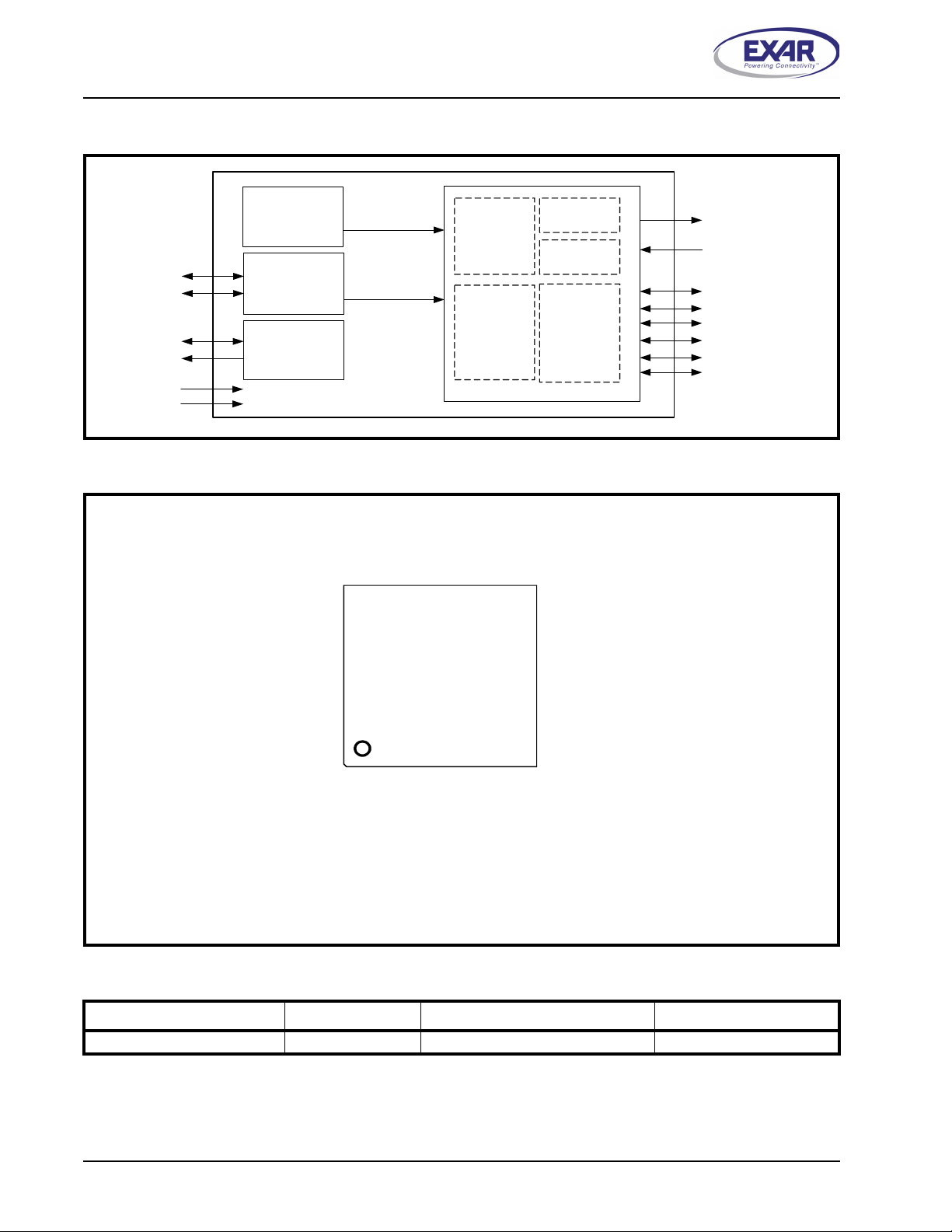
FIGURE 1. XR21V1410 BLOCK DIAGRAM
Internal
48MHz
Oscillator
USBD+
USBD-
SDA
SCL
3.3V VCC
GND
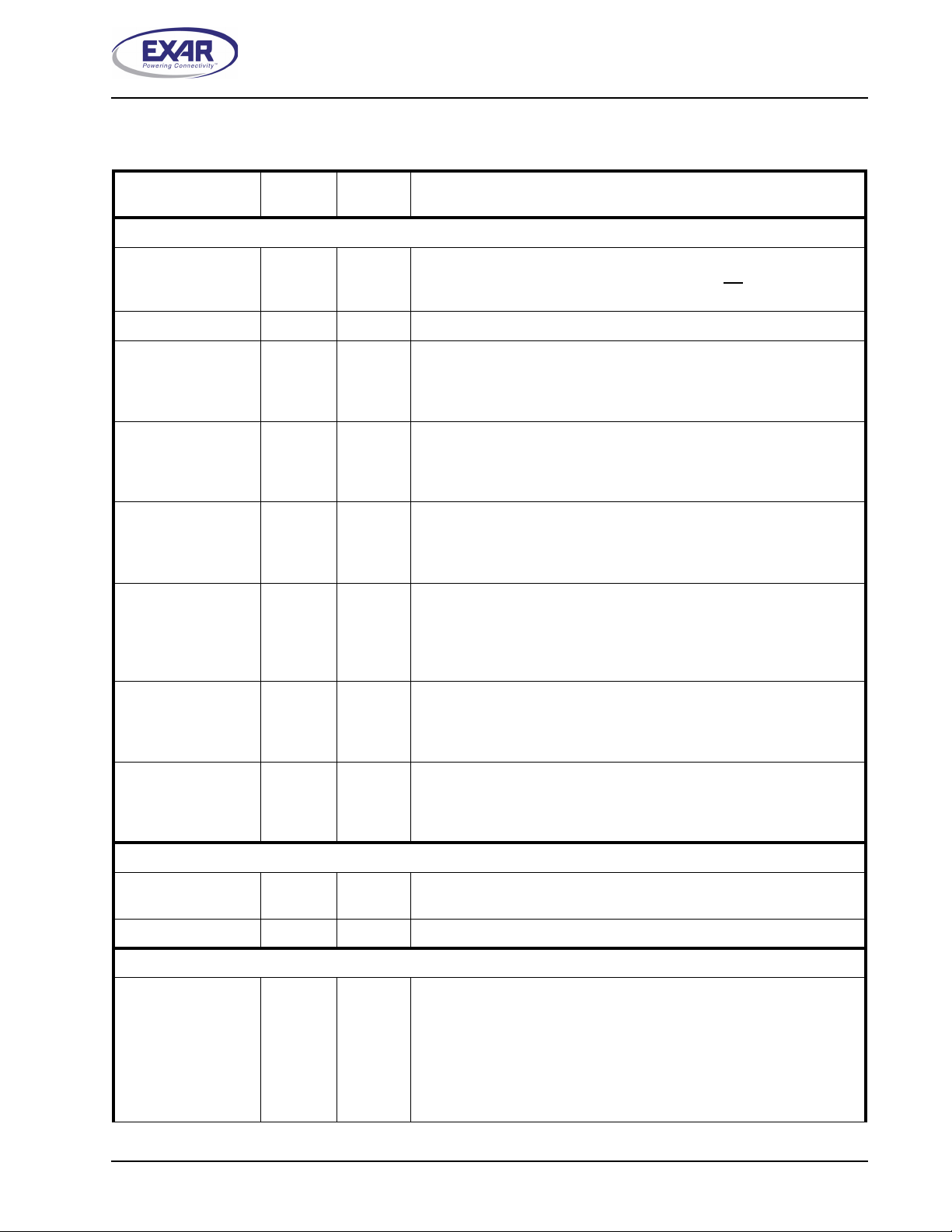
FIGURE 2. PIN OUT ASSIGNMENT
USB Slave
Interface
I2C
Interface
GND
SDA
SCL
12 11 10 9
13
Fractional
BRG
Internal
Status and
Control
Registers
RX
TX
8
128-byte
TX FIFO
384-byte
RX FIFO
GPIOs/
Modem IO
UART
GPIO0/RI#
TX
RX
GPIO5/RTS#
GPIO4/CTS#
GPIO3/DTR#
GPIO2/DSR#
GPIO1/CD#
GPIO0/RI#
USBD-
USBD+
ORDERING INFORMATION
PART NUMBER PACKAGE OPERATING TEMPERATURE RANGE DEVICE STATUS
XR21V1410IL16 16-pin QFN -40°C to +85°C Active
VCC
14
15
16-Pin
QFN
16
1234
GND
LOWPOWER
7
GPIO1/CD#
6
GPIO2/DSR#
5
GPIO3/DTR#
GPIO5/RTS#
GPIO4/CTS#
2
XR21V1410
REV. 1.0.0 1-CH FULL-SPEED USB UART
PIN DESCRIPTIONS
Pin Description
NAME
UART Signals
RX 10 I
TX 9 O
GPIO0/RI#
GPIO1/CD#
GPIO2/DSR#
GPIO3/DTR#
GPIO4/CTS#
16-QFN
PIN #
8 I/O
7 I/O
6 I/O
5 I/O
4 I/O
TYPE DESCRIPTION
UART Channel A Receive Data or IR Receive Data. This pin has an
internal pull-up resistor. Internal pull-up resistor is
suspend mode.
UART Channel A Transmit Data or IR Transmit Data.
General purpose I/O or UART Ring-Indicator input (active low). This pin
has an internal pull-up resistor. Internal pull-up resistor is disabled during
suspend mode. If using this GPIO as an input, a pull-up resistor is
required to minimize the power consumption in the suspend mode.
General purpose I/O or UART Carrier-Detect input (active low). This pin
has an internal pull-up resistor. Internal pull-up resistor is disabled during
suspend mode. If using this GPIO as an input, a pull-up resistor is
required to minimize the power consumption in the suspend mode.
General purpose I/O or UART Data-Set-Ready input (active low). This
pin has an internal pull-up resistor. Internal pull-up resistor is disabled
during suspend mode. If using this GPIO as an input, a pull-up resistor
is required to minimize the power consumption in the suspend mode.
General purpose I/O or UART Data-Terminal-Ready output (active low).
This pin has an internal pull-up resistor. Internal pull-up resistor is dis
abled during suspend mode. If using this GPIO as an input, a pull-up
resistor is required to minimize the power consumption in the suspend
mode.
General purpose I/O or UART Clear-to-Send input (active low). This pin
has an internal pull-up resistor. Internal pull-up resistor is disabled during
suspend mode. If using this GPIO as an input, a pull-up resistor is
required to minimize the power consumption in the suspend mode.
not disabled during
-
GPIO5/RTS#
USB Interface Signals
USBD+ 15 I/O
USBD- 14 I/O
I2C Interface Signals
SDA 11 OD
3 I/O
General purpose I/O or UART Request-to-Send output (active low). This
pin has an internal pull-up resistor. Internal pull-up resistor is disabled
during suspend mode. If using this GPIO as an input, a pull-up resistor
is required to minimize the power consumption in the suspend mode.
USB port differential data plus. This pin has a 1.5 K Ohm internal pull-up
resistor.
USB port differential data minus.
I2C-controller data input/output (open-drain). 1K pull-up resistor is
required. An optional external I
default configurations upon power-up including the USB Vendor ID and
Device ID.
If an EEPROM is not used, this pin can be used with the SCL pin to
select the Remote Wake-up and Power modes. An external pull-up or
pull-down resistor is required. See
2
C EEPROM can be used to store
Table 1
3

XR21V1410
1-CH FULL-SPEED USB UART REV. 1.0.0
Pin Description
NAME
SCL 12 I
Ancillary Signals
LOWPOWER
VCC
GND
NOTE: Pin type: I=Input, O=Output, I/O= Input/output, OD=Output Open Drain.
16-QFN
PIN #
2 O
16 Pwr
1, 13 Pwr
YPE DESCRIPTION
T
I2C-controller serial input clock. 1K pull-up resistor is required. An
optional external I
tions upon power-up including the USB Vendor ID and Device ID.
If an EEPROM is not used, this pin can be used with the SDA pin to
select the Remote Wake-up and Power modes. An external pull-up or
pull-down resistor is required. See Table 1
Low power status output. This pin is HIGH when the XR21V1410 is in
the suspend mode. This pin is LOW when the XR21V1410 is not in the
suspend mode. An external pull-up or pull-down resistor is required on
this pin. This pin is sampled upon power-on to configure the polarity of
the LOWPOWER output during suspend mode. An external pull-up
resistor will cause the LOWPOWER pin to be HIGH during suspend
mode. An external pull-down resistor will cause the LOWPOWER pin to
be LOW during suspend mode.
+3.3V power supply. All inputs are 5V tolerant.
Power supply common, ground.
2
C EEPROM can be used to store default configura-
4
XR21V1410
REV. 1.0.0 1-CH FULL-SPEED USB UART
1.0 FUNCTIONAL DESCRIPTIONS
1.1 USB interface
The USB interface of the V1410 is compliant with the USB 2.0 Full-Speed Specifications. The USB
configuration model presented by the V1410 to the device driver is compatible to the Abstract Control Model of
the USB Communication Device Class (CDC-ACM). The V1410 uses the following set of parameters:
• 1 Control Endpoint
■ Endpoint 0 as outlined in the USB specifications
• 1 Configuration is supported
• 2 interfaces for the UART channel
■ Single interrupt endpoint
■ Bulk-in and bulk-out endpoints
1.1.1 USB Vendor ID
Exar’s USB Vendor ID is 0x04E2. This is the default Vendor ID that is used for the V1410 unless a valid
EEPROM is present on the I2C interface signals. If a valid EEPROM is present, the Vendor ID from the
EEPROM will be used.
1.1.2 USB Product ID
The default USB Product ID for the V1410 is 0x1410. If a valid EEPROM is present, the Product ID from the
EEPROM will be used.
1.2 I2C Interface
The I2C interface provides connectivity to an external I2C memory device (i.e. EEPROM) that can be read by
the V1410 for configuration.
The SDA and SCL are used to specify whether Remote Wakeup and/or Bus Powered configurations are to be
supported. These pins are sampled at power-up. The following table describes how Remote Wakeup and Bus
Powered support.
TABLE 1: REMOTE WAKEUP AND POWER MODES
SDA SCL
1 1 No Self-Powered Default, if no EEPROM is present
1 0 No Bus-Powered
0 1 Yes Self-Powered
0 0 Yes Bus-Powered
REMOTE WAKE-UP
UPPORT
S
POWER MODE COMMENTS
5
XR21V1410
1-CH FULL-SPEED USB UART REV. 1.0.0
1.2.1 EEPROM Contents
The I2C address should be 0xA0. An EEPROM can be used to override default Vendor IDs and Device IDs, as
well as other attributes and maximum power consumption. The EEPROM must contain 8 bytes of data as
specified in
Table 2
TABLE 2: EEPROM CONTENTS
EEPROM
ADDRESS
0 Vendor ID (LSB)
1 Vendor ID (MSB)
2 Product ID (LSB)
3 Product ID (MSB)
4 Device Attributes
5 Device Maximum Power
6 Reserved
7 Signature of 0x58 (’X’). If the signature is not correct, the contents of the EEPROM are ignored.
CONTENTS
These values are uploaded from the EEPROM to the corresponding USB Standard Device Descriptor or
Standard Configuration Descriptor. For details of the USB Descriptors, refer to the USB 2.0 specifications.
1.2.1.1 Vendor ID
The Vendor ID value replaces the idVendor field in the USB Standard Device Descriptor.
1.2.1.2 Product ID
The Product ID value replaces the idProduct field in the USB Standard Device Descriptor.
1.2.1.3 Device Attributes
The Device Attributes value replaces the bmAttributes field in the USB Standard Configuration Descriptor.
1.2.1.4 Device Maximum Power
The Device Maximum Power value replaces the bMaxPower field in the USB Standard Configuration
Descriptor.
1.3 UART Manager
The UART Manager enables/disables the UART including the TX and RX FIFOs. The UART Manager is
located in a separate register block from the UART registers.
1.4 UART
The UART can be configured via USB control transfers from the USB host.
1.4.1 Transmitter
The transmitter consists of a 128-byte TX FIFO and a Transmit Shift Register (TSR). Once a bulk-out packet
has been received and the CRC has been validated, the data bytes in that packet are written into the TX FIFO
of the specified UART channel. Data from the TX FIFO is transferred to the TSR when the TSR is idle or has
completed sending the previous data byte. The TSR shifts the data out onto the TX output pin at the data rate
defined by the CLOCK_DIVISOR and TX_CLOCK_MASK registers. The transmitter sends the start bit
followed by the data bits (starting with the LSB), inserts the proper parity-bit if enabled, and adds the stopbit(s). The transmitter can be configured for 7 or 8 data bits with parity or 9 data bits with no parity.
1.4.1.1 9-Bit Data Mode
6

XR21V1410
REV. 1.0.0 1-CH FULL-SPEED USB UART
In 9-bit data mode, two bytes of data must be written. The first byte that is loaded into the TX FIFO are the first
8 bits (data bits 7-0) of the 9-bit data. Bit-0 of the second byte that is loaded into the TX FIFO is bit-8 of the 9bit data. The data that is transmitted on the TX pin is as follows: start bit, 9-bit data, stop bit.
1.4.2 Receiver
The receiver consists of a 384-byte RX FIFO and a Receive Shift Register (RSR). Data that is received in the
RSR via the RX pin is transferred into the RX FIFO along with any error tags such as Framing, Parity, Break
and Overrun errors. Data from the RX FIFO can be sent to the USB host by sending a bulk-in packet.
1.4.2.1 Character Mode
In character mode, up to 64 bytes of data can be sent at a time to the USB host.
1.4.2.2 Character + Status Mode
In this mode, each 8-bit character and the 4 error bits associated with it can be transmitted to the USB host.
The 4 error bits will be in the second byte following the 8-bit character. In this mode, up to 32 character bytes
are sent per bulk-in packet.
1.4.2.3 9-Bit Data Mode
In 9-bit data mode, two bytes of data are sent to the USB host for each byte 9-bit data that is received. The first
byte sent to the USB host is the first 8-bits of data. Bit-0 of the second byte is the bit-9 of the data.
1.4.3 GPIO
Each UART has 6 GPIOs. By default, the GPIOs are general purpose I/Os. However, there are few modes
that can be enabled to add additional feature such as Auto RTS/CTS Flow control, Auto DTR/DSR Flow
Control or Transceiver Enable Control. See
1.4.4 Automatic RTS/CTS Hardware Flow Control
GPIO5 and GPIO4 of the UART channel can be enabled as the RTS# and CTS# signals for Auto RTS/CTS
flow control when GPIO_MODE[2:0] = ’001’ and FLOW_CONTROL[2:0] = ’001’. Automatic RTS flow control is
used to prevent data overrun errors in local RX FIFO by de-asserting the RTS signal to the remote UART.
When there is room in the RX FIFO, the RTS pin will be re-asserted. Automatic CTS flow control is used to
prevent data overrun to the remote RX FIFO. The CTS# input is monitored to suspend/restart the local
transmitter (see
Figure 3):
Table 13.
7
 Loading...