

EXAR XR16M781 Service Manual
XR16M781
1.62V TO 3.63V UART WITH 64-BYTE FIFO AND VLIO INTERFACE
AUGUST 2009 REV. 1.0.1
GENERAL DESCRIPTION
The XR16M7811 (M781) is an enhanced Universal
Asynchronous Receiver and Transmitter (UART) with
a VLIO bus interface and has 64 bytes of transmit
and receive FIFOs, programmable transmit and
receive FIFO trigger levels, automatic hardware and
software flow control, and data rates of up to 20 Mbps
at 3.3V, 16 Mbps at 2.5V and 10 Mbps at 1.8V with
4X data sampling rate.
The Auto RS-485 Half-Duplex Direction control
feature simplifies both the hardware and software for
half-duplex RS-485 applications. In addition, the
Multidrop mode with Auto Address detection
increases the performance by simplifying the
software routines.
The Independent TX/RX Baud Rate Generator
feature allows the transmitter and receiver to operate
at different baud rates. Power consumption of the
M781 can be minmized by enabling the sleep mode
and PowerSave mode.
The M781 has a 16550 compatible register set that
provide users with operating status and control,
receiver error indications, and modem serial interface
controls. An internal loopback capability allows
onboard diagnostics. The M781 is available in 24-pin
QFN, 32-pin QFN and 25-pin BGA packages.
NOTE: 1 Covered by U.S. Patent #5,649,122.
FEATURES
• VLIO bus interface
• Pin-to-pin compatible with SC16C850V and
SC16C850SV in 32-QFN package
• 20 Mbps maximum data rate
• Programmable TX/RX FIFO Trigger Levels
• TX/RX FIFO Level Counters
• Independent TX/RX Baud Rate Generator
• Fractional Baud Rate Generator
• Auto RTS/CTS Hardware Flow Control
• Auto XON/XOFF Software Flow Control
• Auto RS-485 Half-Duplex Direction Control
• Multidrop mode w/ Auto Address Detect
• Sleep Mode with Automatic Wake-up
• PowerSave mode
• Infrared (IrDA 1.0 and 1.1) mode
• 1.62V to 3.63V supply operation
• Crystal oscillator or external clock input
APPLICATIONS
• Personal Digital Assistants (PDA)
• Cellular Phones/Data Devices
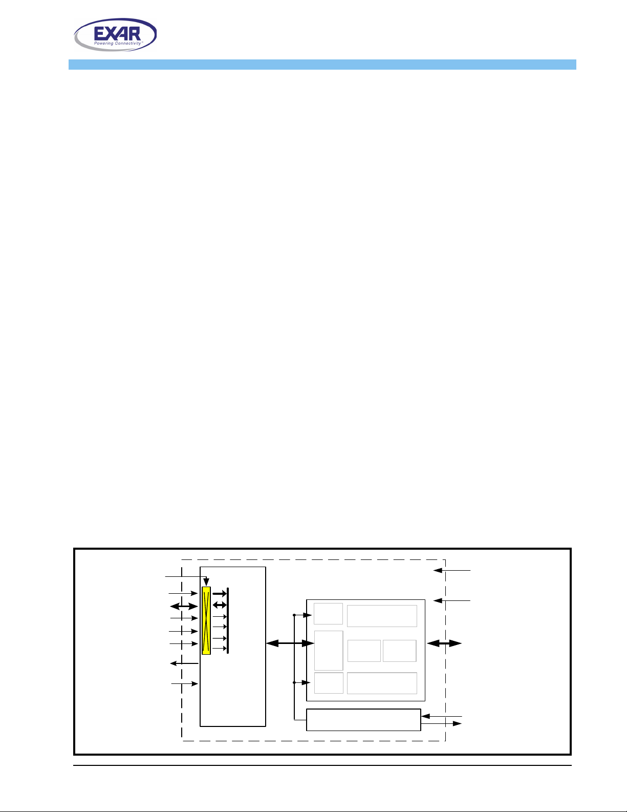
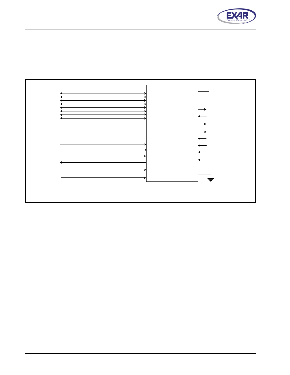
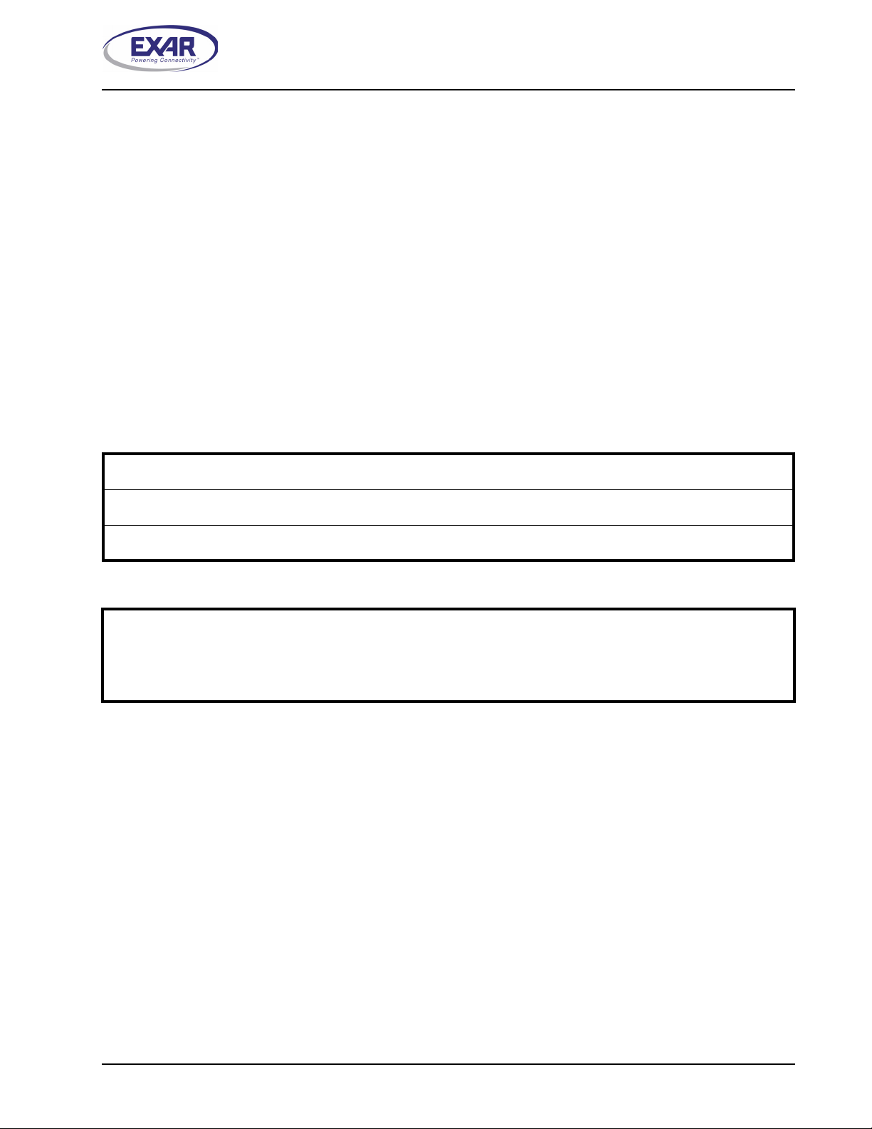
FIGURE 1. XR16M781 BLOCK DIAGRAM
PwrSave
LLA#
AD7:AD0
IOR#
IOW #
CS#
INT
RESET#
VLIO Bus
Interface
• Battery-Operated Devices
• Global Positioning System (GPS)
• Bluetooth
TX
64 Byte TX FIFO
BRG
UART
ENDEC
Regs
RX
64 B yte RX FIF O
BRG
Crystal Osc/Buffer
IR
TX &
RX
VCC
(1.62 to 3.63 V)
GND
TX, RX,
RTS#, CTS#,
DTR#, DSR#,
RI#, CD#
XTAL1
XTAL2
Exar Corporation 48720 Kato Road, Fremont CA, 94538 • (510) 668-7000 • FAX (510) 668-7017 • www.exar.com
XR16M781
1.62V TO 3.63V UART WITH 64-BYTE FIFO AND VLIO INTERFACE REV. 1.0.1
FIGURE 2. PIN OUT ASSIGNMENT
RESET#
RTS#
INT
CTS#
18 17 16 15 14 13
VCC
19
AD0
20
AD1
21
22
AD2
23
AD3
24
AD4
123456
RTS#
RESET#
24-pin QFN
AD6
AD5
DTR#
25
26
27
28
29
30
31
32
CTS#
24
23
22 21 20 19
32-pin QFN
23456
1
NC
AD4
AD5
INT
LLA#
NC
IOR#
12
GND
11
IOW#
10
9
XTAL2
8
XTAL1
7
PWRSAVE
TX
RX
AD7
CS#
DSR#
CD#
RI#
VCC
AD0
AD1
AD2
AD3
AD6
LLA#NCNC
RXTXCS
AD7
18
17
78
NC
16
15
NC
14
IOR#
13
GND
12
IOW#
XTAL2
11
XTAL1
10
9
PWRSAVE
ORDERING INFORMATION
PART NUMBER PACKAGE
XR16M781IL24 24-Pin QFN -40°C to +85°C Active
A1 Corner
1 2 3 4 5
A
B
C
D
E
Transparent Top View
CTS# RESET# RTS# LLA# IOR#
VCC AD5 DTR# INT GND
AD0 AD7 RX DSR# XTAL2
AD3 AD1 CS# PWRSAVE XTAL1
AD4 AD2 AD6 TX IOW#
OPERATING TEMPERATURE
ANGE
R
DEVICE STATUS
XR16M781IL32 32-Pin QFN -40°C to +85°C Active
XR16M781IB25 25-Pin BGA -40°C to +85°C Active
2
XR16M781
REV. 1.0.1 1.62V TO 3.63V UART WITH 64-BYTE FIFO AND VLIO INTERFACE
PIN DESCRIPTIONS
Pin Description
NAME
DATA BUS INTERFACE
AD0
AD1
AD2
AD3
AD4
AD5
AD6
AD7
IOR# 12 14 A5 I
IOW# 10 12 E5 I
CS# 6 8 D3 I
LLA# 14 19 A4 I
INT 15 20 B4 O
24-QFN
PIN#
20
21
22
23
24
32-QFN
PIN#
29
30
31
32
1
2
3
25-BGA
PIN#
C1
D2
E2
D1
1
3
4
5
E1
B2
E3
C2
TYPE DESCRIPTION
I/O
Multiplexed Address/Data lines [7:0]. The register address is
latched on the rising edge of the LLA#. After the LLA# signal goes
high, the UART enters the data phase where the data is placed on
these lines.
Read strobe (active low). The falling edge instigates an internal
read cycle and retrieves the data byte from an internal register
pointed by the latched address. The UART places the data byte on
the data bus to allow the host processor to read it on the rising
edge.
Write strobe (active low). The falling edge instigates the internal
write cycle and the rising edge transfers the data byte on the data
bus to an internal register pointed by the latched address.
Chip select (active low). The falling edge starts the access to the
UART. A read or write is determined by the IOR# and IOW# sig
nals.
Latch Lower Address (active low). The register address is latched
on the rising edge of the LLA# signal. After the LLA# goes high, the
device enters the data phase where the data is placed on the
AD[7:0] lines.
Interrupt output (active high). The output state is defined by the
user through the software setting of MCR[3]. INT is set to the active
mode when MCR[3] is set to a logic 1. INT is set to the three state
mode when MCR[3] is set to a logic 0. See MCR[3].
-
MODEM OR SERIAL I/O INTERFACE
TX 5 7 E4 O
RX 4 6 C3 I
RTS# 16 21 A3 O
UART Transmit Data or infrared encoder data. Standard transmit
and receive interface is enabled when MCR[6] = 0. In this mode,
the TX signal will be a logic 1 during reset or idle (no data). Infrared
IrDA transmit and receive interface is enabled when MCR[6] = 1. In
the Infrared mode, the inactive state (no data) for the Infrared
encoder/decoder interface is a logic 0. If it is not used, leave it
unconnected.
UART Receive Data or infrared receive data. Normal receive data
input must idle at logic 1 condition. The infrared receiver idles at
logic 0. This input should be connected to VCC when not used.
UART Request-to-Send (active low) or general purpose output.
This output must be asserted prior to using auto RTS flow control,
see EFR[6], MCR[1] and IER[6]. This pin can also be used as the
Auto RS-485 Half-duplex Direction control output, see FCTR[3] and
EMSR[3].
3
XR16M781
1.62V TO 3.63V UART WITH 64-BYTE FIFO AND VLIO INTERFACE REV. 1.0.1
Pin Description
NAME
CTS# 18 24 A1 I
DTR# - 22 B3 O
DSR# - 25 C4 I
CD# - 26 - I
RI# - 27 - I
ANCILLARY SIGNALS
XTAL1 8 10 D5 I
XTAL2 9 11 C5 O
PwrSave 7 9 D4 I
RESET# 17 23 A2 O
VCC 19 28 B1 Pwr
24-QFN
PIN#
32-QFN
PIN#
25-BGA
PIN#
YPE DESCRIPTION
T
UART Clear-to-Send (active low) or general purpose input. It can
be used for auto CTS flow control, see EFR[7], MSR[4] and IER[7].
This input should be connected to VCC when not used.
UART Data-Terminal-Ready (active low) or general purpose output.
UART Data-Set-Ready (active low) or general purpose input. This
input should be connected to VCC when not used.
UART Carrier-Detect (active low) or general purpose input. This
input should be connected to VCC when not used.
UART Ring-Indicator (active low) or general purpose input. This
input should be connected to VCC when not used.
Crystal or external clock input.
Crystal or buffered clock output.
Power-Save (active high). This feature isolates the M781’s data bus
interface from the host preventing other bus activities that cause
higher power drain during sleep mode. See Sleep Mode with Auto
Wake-up and Power-Save Feature section for details. This pin does
not have an internal pull-down resistor. This input should be con
nected to GND when not used.
Device reset (active low). A 40 ns minimum LOW pulse on this pin
will reset the internal registers and all outputs of the UART. The
UART transmitter output will be held HIGH, the receiver input will
be ignored and outputs are reset during reset period (see UART
Reset Conditions).
1.62V to 3.63V power supply.
-
GND 11 13 B5 Pwr
GND Center
Pad
NC 13 2, 15-18 - -
Pin type: I=Input, O=Output, I/O= Input/output, OD=Output Open Drain.
Center
Pad
- Pwr
Power supply common, ground.
The center pad on the backside of the QFN package is metallic and
should be connected to GND on the PCB. The thermal pad size on
the PCB should be the approximate size of this center pad and
should be solder mask defined. The solder mask opening should be
at least 0.0025" inwards from the edge of the PCB thermal pad.
No Connects.
4

XR16M781
REV. 1.0.1 1.62V TO 3.63V UART WITH 64-BYTE FIFO AND VLIO INTERFACE
1.0 PRODUCT DESCRIPTION
The XR16M781 (M781) is a high performance single-channel UART with a VLIO bus interface. It has its set of
device configuration registers. The configuration registers set is 16550 UART compatible for control, status
and data transfer. Additionally, the M781 channel has 64 bytes of transmit and receive FIFOs, Automatic RTS/
CTS Hardware Flow Control, Automatic Xon/Xoff and Special Character Software Flow Control, infrared
encoder and decoder (IrDA ver 1.0 and 1.1), programmable fractional baud rate generator with a prescaler of
divide by 1 or 4, and data rate up to 20 Mbps. The XR16M781 can operate from 1.62 to 3.63 volts. The M781
is fabricated with an advanced CMOS process.
Larger FIFO
The M781 provides a solution that supports 64 bytes of transmit and receive FIFO memory, instead of 16 bytes
in the XR16L580. The M781 is designed to work with high performance data communication systems, that
requires fast data processing time. Increased performance is realized in the M781 by the larger transmit and
receive FIFOs, FIFO trigger level control and automatic flow control mechanism. This allows the external
processor to handle more networking tasks within a given time. For example, the XR16L580 with a 16 byte
FIFO, unloads 16 bytes of receive data in 1.53 ms (This example uses a character length of 11 bits, including
start/stop bits at 115.2Kbps). This means the external CPU will have to service the receive FIFO at 1.53 ms
intervals. However with the 64 byte FIFO in the M781, the data buffer will not require unloading/loading for 6.1
ms. This increases the service interval giving the external CPU additional time for other applications and
reducing the overall UART interrupt servicing time. In addition, the programmable FIFO level trigger interrupt
and automatic hardware/software flow control is uniquely provided for maximum data throughput performance
especially when operating in a multi-channel system. The combination of the above greatly reduces the CPU’s
bandwidth requirement, increases performance, and reduces power consumption.
Data Rate
The M781 is capable of operation up to 20 Mbps at 3.3V with 4X internal sampling clock rate. The device can
operate at 3.3V with a 24 MHz crystal on pins XTAL1 and XTAL2, or external clock source of 80 MHz on XTAL1
pin. With a typical crystal of 14.7456 MHz and through a software option, the user can set the prescaler bit and
sampling rate for data rates of up to 3.68 Mbps.
Enhanced Features
The rich feature set of the M781 is available through the internal registers. Automatic hardware/software flow
control, programmable transmit and receive FIFO trigger levels, selectable baud rates, infrared encoder/
decoder, modem interface controls, and a sleep mode are all standard features. MCR bit-5 provides a facility
for turning off (Xon) software flow control with any incoming (RX) character. The M781 includes new features
such as 9-bit (Multidrop) mode, auto RS-485 half-duplex direction control, different baud rate for TX and RX,
fast IR mode and fractional baud rate generator.
5
XR16M781
1.62V TO 3.63V UART WITH 64-BYTE FIFO AND VLIO INTERFACE REV. 1.0.1
2.0 FUNCTIONAL DESCRIPTIONS
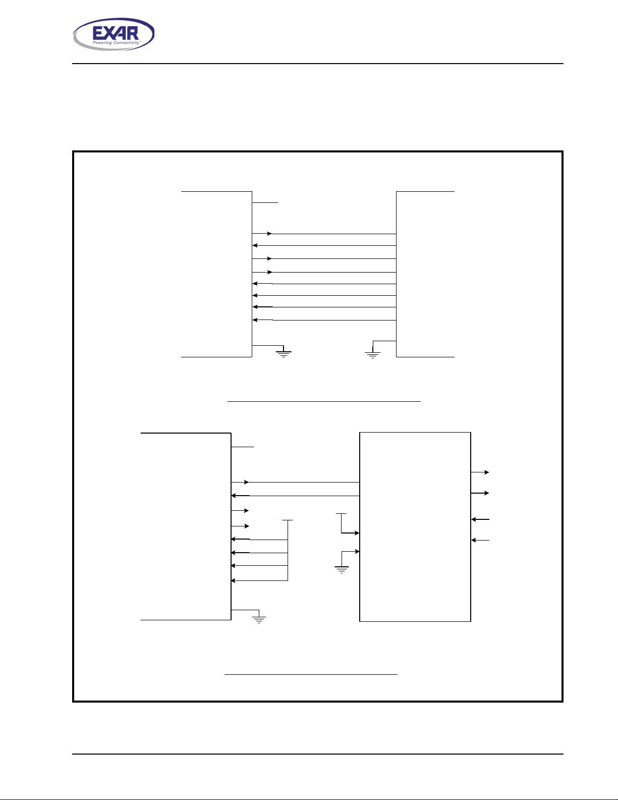
2.1 CPU Interface
The CPU interface is a VLIO bus interface. The VLIO bus interface is an 8-bit multiplexed address/data bus
interface. Each bus cycle is asynchronous using CS#, LLA# and IOR# or IOW# inputs. A typical data bus
interconnection for the VLIO bus interface is shown in
FIGURE 3. XR16M781 TYPICAL VLIO DATA BUS INTERCONNECTIONS
Figure 3.
AD0
AD1
AD2
AD3
AD4
AD5
AD6
AD7
UART_IOR#
UART_IOW#
UART_CS#
UART_INT
POWERSAVE
UART_RESET# RESET#
AD0
AD1
AD2
AD3
AD4
AD5
AD6
AD7
IOR#
IOW#
CS#
INT
PWRSAVE
TX
RX
DTR#
RTS#
CTS#
DSR#
CD#
RI#
GND
VCCVCC
Serial Transceivers of
RS-232
RS-485
RS-422
Or Infrared
6
XR16M781
REV. 1.0.1 1.62V TO 3.63V UART WITH 64-BYTE FIFO AND VLIO INTERFACE
2.2 Serial Interface
The M781 is typically used with RS-232, RS-485 and IR transceivers. The following figure shows typical
connections from the UART to the different transceivers. For more information on RS-232 and RS-485/422
transceivers, go to www.exar.com or send an e-mail to uarttechsupport@exar.com.
FIGURE 4. XR16M781 TYPICAL SERIAL INTERFACE CONNECTIONS
UART
UART
VCCVCC
TX
RX
DTR#
RTS#
CTS#
DSR#
CD#
RI#
GND
R S -23 2 F ull-M o dem S eria l In terface
NC
NC
VCC
DI
RO
VCC
VCC
DE
RE#
VCC
TX
RX
RTS#
DTR#
CTS#
DSR#
CD
RI
#
#
RS-232
Transceiver
T1IN
R1OUT
T2IN
T3IN
R2OUT
R3OUT
R4OUT
R5OUT
GND
RS-485
Transceiver
Full-duplex
TX+
TX-
RX+
RX-
GND
RS-485 Full-Duplex Serial Interface
7
XR16M781
1.62V TO 3.63V UART WITH 64-BYTE FIFO AND VLIO INTERFACE REV. 1.0.1
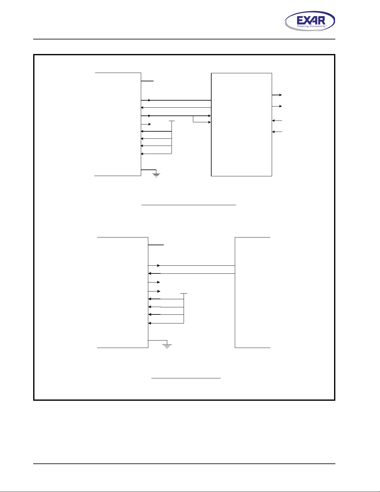
FIGURE 5. XR16M781 TYPICAL SERIAL INTERFACE CONNECTIONS
UART
NC
VCC
VCC
VCC
RTS#
DTR#
CTS#
DSR#
CD
RI
GND
TX
RX
#
#
RS-485 Half-Duplex Serial Interface
VCCVCC
DI
RO
DE
RE#
RS-485
Transceiver
Half-duplex
Transceiver
Y
Z
A
B
IR
UART
TX
RX
DTR#
RTS#
CTS#
DSR#
CD#
RI#
GND
NC
NC
VCC
Infrared Connection
TXD
RXD
8
XR16M781
REV. 1.0.1 1.62V TO 3.63V UART WITH 64-BYTE FIFO AND VLIO INTERFACE
2.3 Device Reset
The RESET# input resets the internal registers and the serial interface outputs to their default state (see
Table 18). An active low pulse of longer than 40 ns duration will be required to activate the reset function in the
device. Following a power-on reset or an external reset, the M781 is software compatible with previous
generation of UARTs.
2.4 Internal Registers
The M781 has a set of 16550 compatible registers for controlling, monitoring and data loading and unloading.
These registers function as data holding registers (THR/RHR), interrupt status and control registers (ISR/IER),
a FIFO control register (FCR), receive line status and control registers (LSR/LCR), modem status and control
registers (MSR/MCR), programmable data rate (clock) divisor registers (DLL/DLM/DLD), and a user accessible
scratchpad register (SPR).
Beyond the general 16C550 features and capabilities, the M781 offers enhanced feature registers (EFR, Xon1/
Xoff 1, Xon2/Xoff 2, DLD, FCTR, EMSR, FC and TRIG) that provide automatic RTS and CTS hardware flow
control, automatic Xon/Xoff software flow control, 9-bit (Multidrop) mode, auto RS-485 half duplex control,
different baud rate for TX and RX and fractional baud rate generator. All the register functions are discussed in
full detail later in
2.5 INT Ouput
The interrupt outputs change according to the operating mode and enhanced features setup. Tab l e 1 and 2
summarize the operating behavior for the transmitter and receiver. Also see Figure 19 through 22.
“Section 3.0, UART INTERNAL REGISTERS” on page 23.
TABLE 1: INT PIN OPERATION FOR TRANSMITTER
FCR BIT-0 = 0 (FIFO DISABLED) FCR BIT-0 = 1 (FIFO ENABLED)
INT Pin LOW = One byte in THR
HIGH = THR empty
TABLE 2: INT PIN OPERATION FOR RECEIVER
FCR BIT-0 = 0 (FIFO DISABLED) FCR BIT-0 = 1 (FIFO ENABLED)
INT Pin HIGH = One byte in RHR
LOW = RHR empty
LOW = FIFO above trigger level
HIGH = FIFO below trigger level or FIFO empty
LOW = FIFO below trigger level
HIGH = FIFO above trigger level or RX Data Timeout
9
XR16M781
1.62V TO 3.63V UART WITH 64-BYTE FIFO AND VLIO INTERFACE REV. 1.0.1
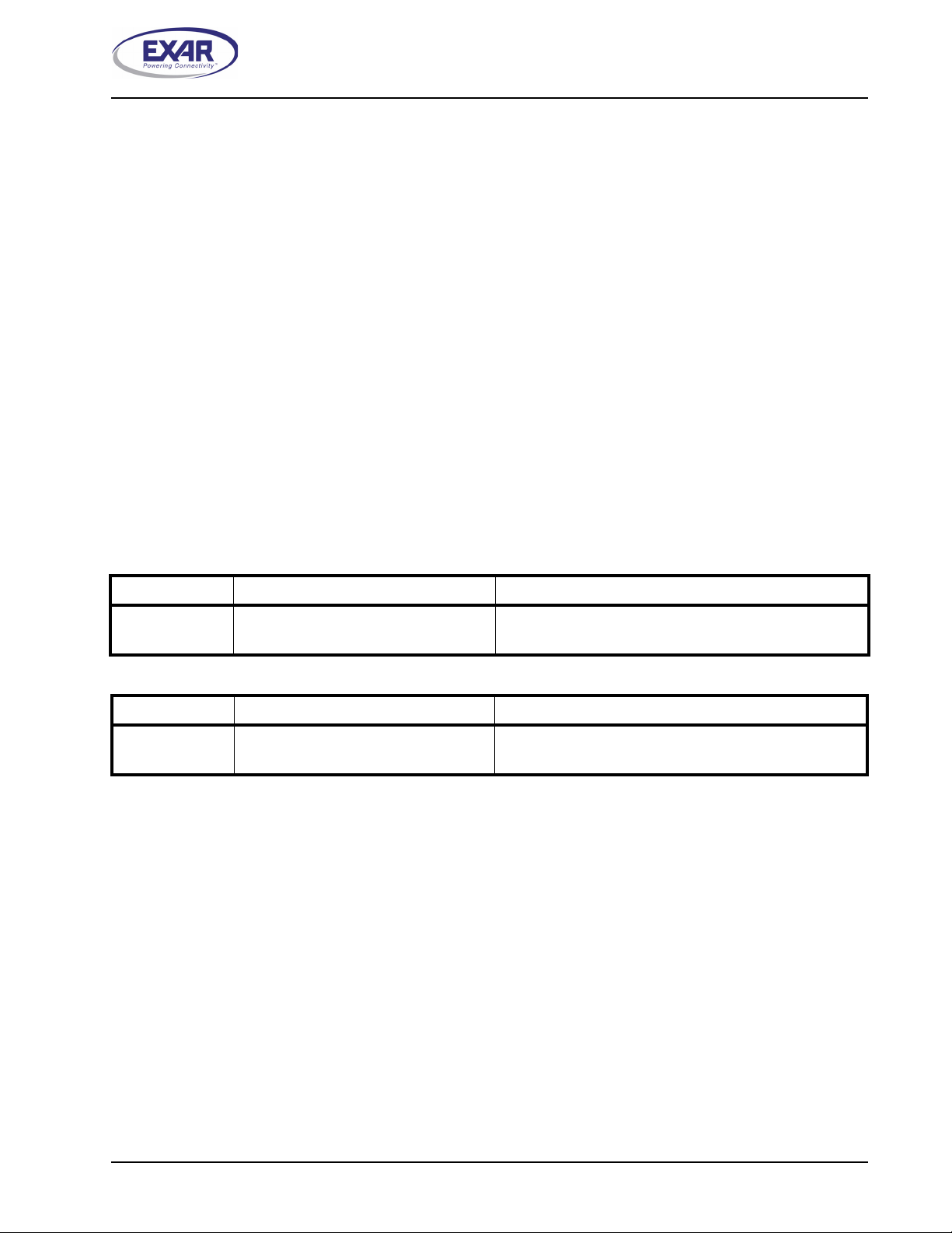
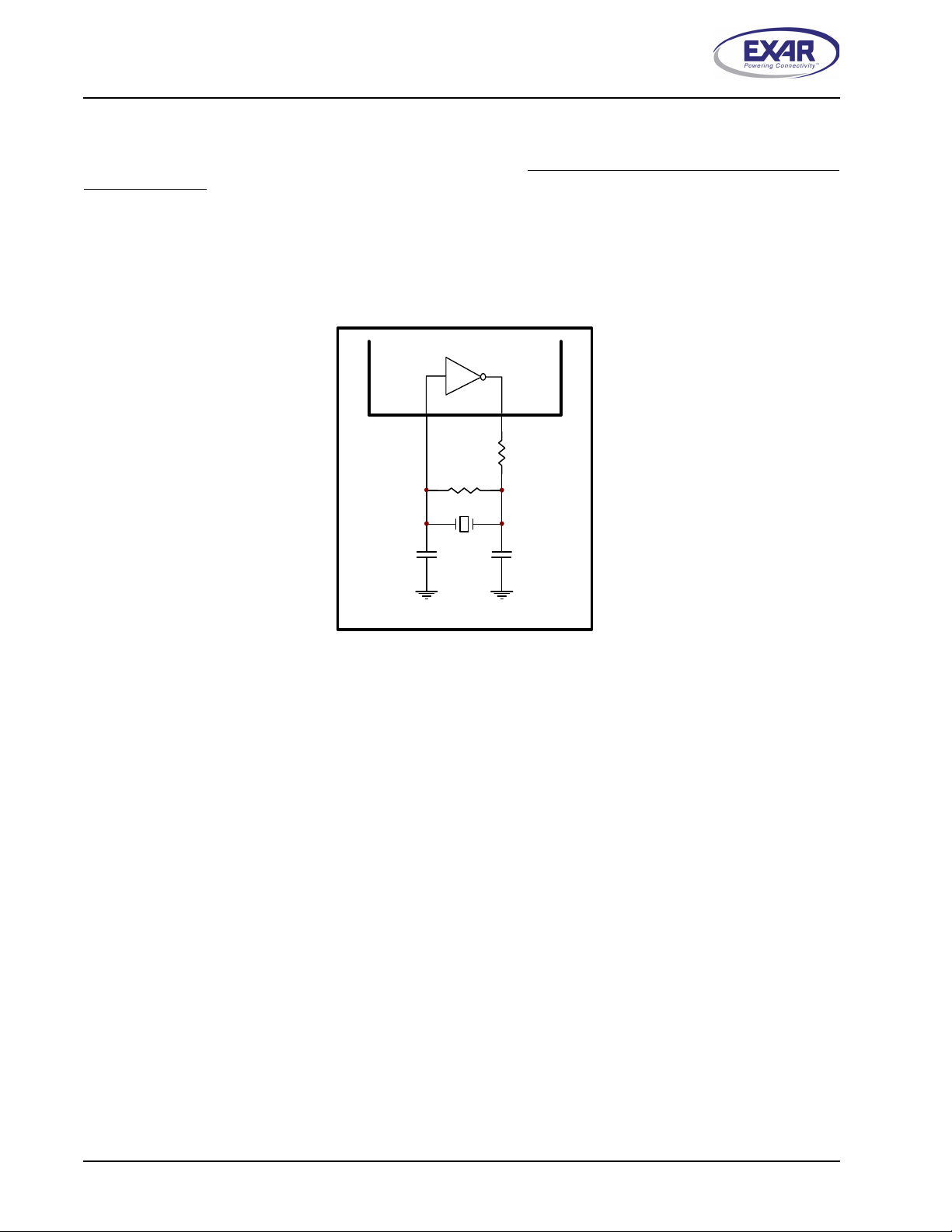
2.6 Crystal Oscillator or External Clock Input
The M781 includes an on-chip oscillator to produce a clock for the baud rate generators in the device when a
crystal is connected between XTAL1 and XTAL2 as show below.
for bus operation. The crystal oscillator provides a system clock to the Baud Rate Generators (BRGs) in the
UART. XTAL1 is the input to the oscillator or external clock buffer input with XTAL2 pin being the output. For
programming details, see
“Section 2.7, Programmable Baud Rate Generator with Fractional Divisor” on
page 11.
FIGURE 6. TYPICAL CRYSTAL CONNECTIONS
The CPU data bus does not require this clock
XTAL 1 XTA L2
R2
500K - 1M
C1
22-47pF
22-47pF
Y1
C2
R1
0-120
(Optional)
1.8432 MHz
to
24 MHz
The on-chip oscillator is designed to use an industry standard microprocessor crystal (parallel resonant,
fundamental frequency with 10-22 pF capacitance load, ESR of 20-120 ohms and 100ppm frequency
tolerance) connected externally between the XTAL1 and XTAL2 pins. Typical oscillator connections are shown
in
Figure 6. Alternatively, an external clock can be connected to the XTAL1 pin to clock the internal baud rate
generator for standard or custom rates. The BGA package has XTAL1 only, the external clock is required. For
further reading on oscillator circuit, see application note DAN108 on EXAR’s web site.
10
XR16M781
REV. 1.0.1 1.62V TO 3.63V UART WITH 64-BYTE FIFO AND VLIO INTERFACE
2.7 Programmable Baud Rate Generator with Fractional Divisor
The M781 has independent Baud Rate Generators (BRGs) with prescalers for the transmitter and receiver.
The prescalers are controlled by a software bit in the MCR register. The MCR register bit-7 sets the prescalers
to divide the input crystal or external clock by 1 or 4. The output of the prescaler clocks to the BRG. The BRG
further divides this clock by a programmable divisor between 1 and (2
16) to obtain a 16X or 8X or 4X sampling clock of the serial data rate. The sampling clock is used by the
transmitter for data bit shifting and receiver for data sampling. For transmitter and receiver, the M781 provides
respective BRG divisors. The BRG divisor (DLL, DLM, and DLD registers) defaults to the value of ’1’ (DLL =
0x01, DLM = 0x00 and DLD = 0x00) upon reset. Therefore, the BRG must be programmed during initialization
to the operating data rate. The DLL and DLM registers provide the integer part of the divisor and the DLD
registers provides the fractional part of the divisor. The four lower bits of the DLD are used to select a value
from 0 (for setting 0000) to 0.9375 or 15/16 (for setting 1111). Programming the Baud Rate Generator
Registers DLL, DLM and DLD provides the capability for selecting the operating data rate.
standard data rates available with a 24MHz crystal or external clock at 16X clock rate. If the pre-scaler is used
(MCR bit-7 = 1), the output data rate will be 4 times less than that shown in
data rates would double. And at 4X sampling rate, they would quadruple. Also, when using 8X sampling mode,
please note that the bit-time will have a jitter (+/- 1/16) whenever the DLD is non-zero and is an odd number.
When using a non-standard data rate crystal or external clock, the divisor value can be calculated with the
following equation(s):
Required Divisor (decimal)=(XTAL1 clock frequency / prescaler) /(serial data rate x 16), with 16X mode, DLD[5:4]=’00’
16
- 0.0625) in increments of 0.0625 (1/
Table 3 shows the
Table 3. At 8X sampling rate, these
Required Divisor (decimal)= (XTAL1 clock frequency / prescaler / (serial data rate x 8), with 8X mode, DLD[5:4] = ’01’
Required Divisor (decimal)= (XTAL1 clock frequency / prescaler / (serial data rate x 4), with 4X mode, DLD[5:4] = ’10’
The closest divisor that is obtainable in the M781 can be calculated using the following formula:
ROUND( (Required Divisor - TRUNC(Required Divisor) )*16)/16 + TRUNC(Required Divisor), where
DLM = TRUNC(Required Divisor) >> 8
DLL = TRUNC(Required Divisor) & 0xFF
DLD = ROUND( (Required Divisor-TRUNC(Required Divisor) )*16)
In the formulas above, please note that:
TRUNC (N) = Integer Part of N. For example, TRUNC (5.6) = 5.
ROUND (N) = N rounded towards the closest integer. For example, ROUND (7.3) = 7 and ROUND (9.9) = 10.
A >> B indicates right shifting the value ’A’ by ’B’ number of bits. For example, 0x78A3 >> 8 = 0x0078.
2.7.1 Independent TX/RX BRG
The XR16M781 has two independent sets of TX and RX baud rate generator. See Figure 7. TX and RX can
work in different baud rate by setting DLD, DLL and DLM register. For example, TX can transmit data to the
remote UART at 9600 bps while RX receives data from remote UART at 921.6 Kbps. For the baud rate setting,
please
See ”Section 4.13, Baud Rate Generator Registers (DLL, DLM and DLD) - Read/Write” on
page 37.
11
XR16M781
1.62V TO 3.63V UART WITH 64-BYTE FIFO AND VLIO INTERFACE REV. 1.0.1
FIGURE 7. BAUD RATE GENERATOR
XTAL1
XTAL2
Crystal
Osc
Buffer
DLD[7]=0
Prescaler
Divide by 1
/
Prescaler
Divide by 4
-
MCR Bit 7=0
(default)
MCR Bit-7=1
DLD[7]=1
DLL
DLM
DLD[5:0]
DLL
DLM
DLD[5:0]
0
1
DLD[6]
16X or 8X or 4X
Sampling Rate Clock
to Transmitter
16X or 8X or 4X
Sampling Rate Clock
to Receiver
TABLE 3: TYPICAL DATA RATES WITH A 24 MHZ CRYSTAL OR EXTERNAL CLOCK AT 16X SAMPLING
Required
Output Data
Rate
400 3750 3750 E A6 0 0
2400 625 625 2 71 0 0
4800 312.5 312 8/16 1 38 8 0
9600 156.25 156 4/16 0 9C 4 0
10000 150 150 0 96 0 0
19200 78.125 78 2/16 0 4E 2 0
25000 60 60 0 3C 0 0
28800 52.0833 52 1/16 0 34 1 0.04
38400 39.0625 39 1/16 0 27 1 0
50000 30 30 0 1E 0 0
57600 26.0417 26 1/16 0 1A 1 0.08
75000 20 20 0 14 0 0
100000 15 15 0 F 0 0
115200 13.0208 13 0 D 0 0.16
153600 9.7656 9 12/16 0 9 C 0.16
200000 7.5 7 8/16 0 7 8 0
225000 6.6667 6 11/16 0 6 B 0.31
230400 6.5104 6 8/16 0 6 8 0.16
250000 6 6 0 6 0 0
300000 5 5 0 5 0 0
400000 3.75 3 12/16 0 3 C 0
460800 3.2552 3 4/16 0 3 4 0.16
500000 3 3 0 3 0 0
750000 2 2 0 2 0 0
921600 1.6276 1 10/16 0 1 A 0.16
1000000 1.5 1 8/16 0 1 8 0
DIVISOR FOR 16x
Clock
(Decimal)
DIVISOR
BTAINABLE IN
O
M781
DLM PROGRAM
ALUE (HEX)
V
DLL PROGRAM
ALUE (HEX)
V
DLD PROGRAM
ALUE (HEX)
V
DATA ERROR
ATE (%)
R
12
XR16M781
REV. 1.0.1 1.62V TO 3.63V UART WITH 64-BYTE FIFO AND VLIO INTERFACE
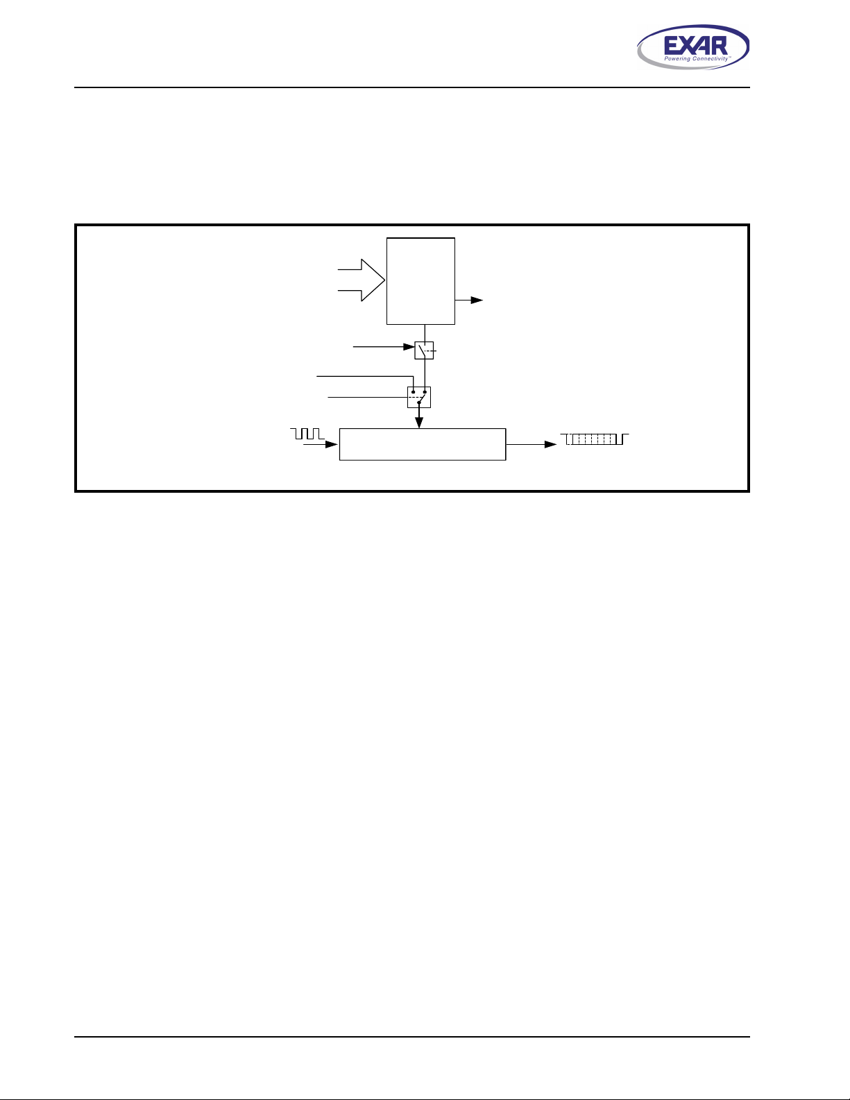
2.8 Transmitter
The transmitter section comprises of an 8-bit Transmit Shift Register (TSR) and 64 bytes of FIFO which
includes a byte-wide Transmit Holding Register (THR). TSR shifts out every data bit with the 16X/8X/4X
internal clock. A bit time is 16/8/4 clock periods. The transmitter sends the start-bit followed by the number of
data bits, inserts the proper parity-bit if enabled, and adds the stop-bit(s). The status of the FIFO and TSR are
reported in the Line Status Register (LSR bit-5 and bit-6).
2.8.1 Transmit Holding Register (THR) - Write Only
The transmit holding register is an 8-bit register providing a data interface to the host processor. The host
writes transmit data byte to the THR to be converted into a serial data stream including start-bit, data bits,
parity-bit and stop-bit(s). The least-significant-bit (Bit-0) becomes first data bit to go out. The THR is the input
register to the transmit FIFO of 64 bytes when FIFO operation is enabled by FCR bit-0. Every time a write
operation is made to the THR, the FIFO data pointer is automatically bumped to the next sequential data
location.
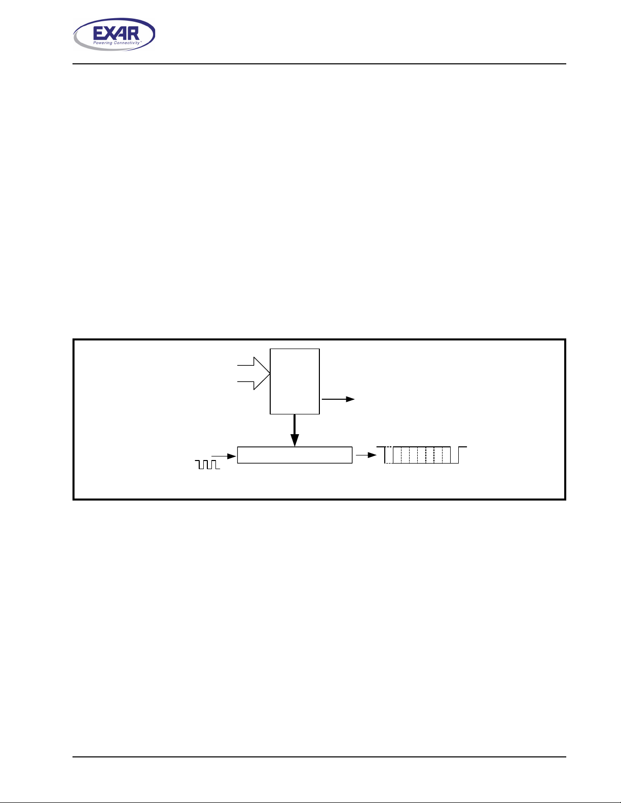
2.8.2 Transmitter Operation in non-FIFO Mode
The host loads transmit data to THR one character at a time. The THR empty flag (LSR bit-5) is set when the
data byte is transferred to TSR. THR flag can generate a transmit empty interrupt (ISR bit-1) when it is enabled
by IER bit-1. The TSR flag (LSR bit-6) is set when TSR becomes completely empty.
FIGURE 8. TRANSMITTER OPERATION IN NON-FIFO MODE
Data
Byte
16X or 8X or 4X
Clock
( DLD[5:4] )
Transmit
Holding
Register
(THR)
Transmit Shift Register (TSR)
THR Interrupt (ISR bit-1)
Enabled by IER bit-1
M
S
B
L
S
B
TXNOFIFO1
13
XR16M781
1.62V TO 3.63V UART WITH 64-BYTE FIFO AND VLIO INTERFACE REV. 1.0.1
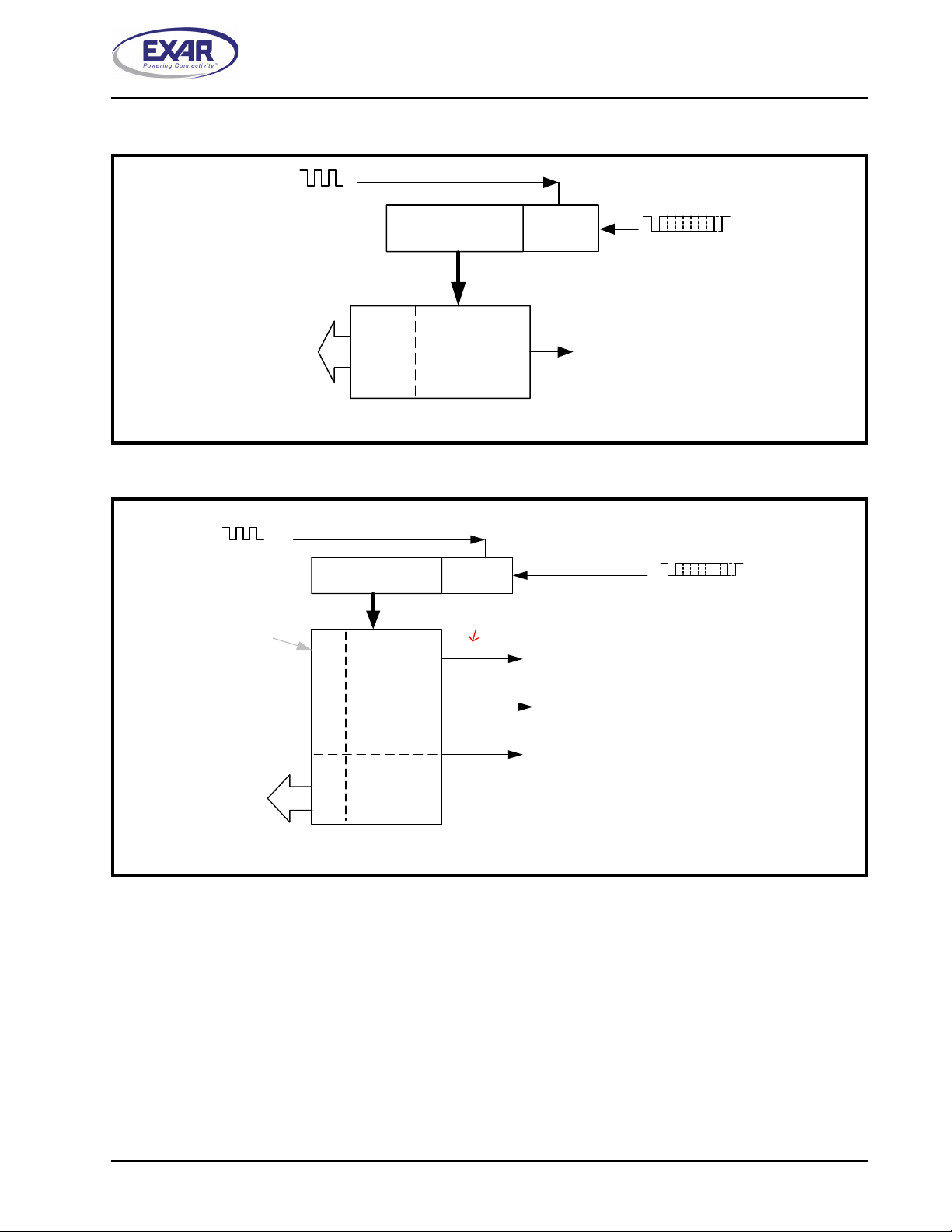
2.8.3 Transmitter Operation in FIFO Mode
The host may fill the transmit FIFO with up to 64 bytes of transmit data. The THR empty flag (LSR bit-5) is set
whenever the FIFO is empty. The THR empty flag can generate a transmit empty interrupt (ISR bit-1) when the
FIFO becomes empty. The transmit empty interrupt is enabled by IER bit-1. The TSR flag (LSR bit-6) is set
when TSR/FIFO becomes empty.
FIGURE 9. TRANSMITTER OPERATION IN FIFO AND FLOW CONTROL MODE
Transmit
Data Byte
Auto CTS Flow Control (CTS# pin)
Flow Control Characters
(Xoff1/2 and Xon1/2 Reg.)
Auto Softw are Flow Co ntrol
16X or 8X or 4X Clock
(DLD[5:4])
Transmit Data Shift Register
Transmit
FIFO
(TSR )
THR Interrupt (ISR bit-1) falls
below the programmed Trigger
Level and then when becomes
empty. FIFO is Enabled by FCR
bit-0=1
TXFIFO1
2.9 Receiver
The receiver section contains an 8-bit Receive Shift Register (RSR) and 64 bytes of FIFO which includes a
byte-wide Receive Holding Register (RHR). The RSR uses the 16X/8X/4X clock (DLD[5:4]) for timing. It
verifies and validates every bit on the incoming character in the middle of each data bit. On the falling edge of
a start or false start bit, an internal receiver counter starts counting at the 16X/8X/4X clock rate. After 8 clocks
(or 4 if 8X or 2 if 4X) the start bit period should be at the center of the start bit. At this time the start bit is
sampled and if it is still a logic 0 it is validated. Evaluating the start bit in this manner prevents the receiver from
assembling a false character. The rest of the data bits and stop bits are sampled and validated in this same
manner to prevent false framing. If there were any error(s), they are reported in the LSR register bits 2-4. Upon
unloading the receive data byte from RHR, the receive FIFO pointer is bumped and the error tags are
immediately updated to reflect the status of the data byte in RHR register. RHR can generate a receive data
ready interrupt upon receiving a character or delay until it reaches the FIFO trigger level. Furthermore, data
delivery to the host is guaranteed by a receive data ready time-out interrupt when data is not received for 4
word lengths as defined by LCR[1:0] plus 12 bits time. This is equivalent to 3.7-4.6 character times. The RHR
interrupt is enabled by IER bit-0. See
Figure 10 and Figure 11 below.
2.9.1 Receive Holding Register (RHR) - Read-Only
The Receive Holding Register is an 8-bit register that holds a receive data byte from the Receive Shift
Register. It provides the receive data interface to the host processor. The RHR register is part of the receive
FIFO of 64 bytes by 11-bits wide, the 3 extra bits are for the 3 error tags to be reported in LSR register. When
the FIFO is enabled by FCR bit-0, the RHR contains the first data character received by the FIFO. After the
RHR is read, the next character byte is loaded into the RHR and the errors associated with the current data
byte are immediately updated in the LSR bits 2-4.
14
XR16M781
REV. 1.0.1 1.62V TO 3.63V UART WITH 64-BYTE FIFO AND VLIO INTERFACE
FIGURE 10. RECEIVER OPERATION IN NON-FIFO MODE
16X or 8X or 4X Clock
( DLD[5:4] )
Receive Data Shift
Register (RSR)
Data Bit
Validation
Receive Data Characters
Receive
Data Byte
and Errors
Error
Tags in
LSR bits
4:2
Receive Data
Holding Register
(RHR)
RHR Interrupt (ISR bit-2)
FIGURE 11. RECEIVER OPERATION IN FIFO AND AUTO RTS FLOW CONTROL MODE
16X or 8X or 4X Clock
( DLD[5:4] )
64 bytes by 11-bit wide
Receive Data
Byte an d E rro rs
FIFO
Receive Data Shift
Register (RSR)
Receive
Data FIFO
(64-sets)
Error Tags
Receive
Data
LSR bits 4:2
Error Tags in
Da ta B it
Va lida tion
Example
- RX FIFO trigger level selected at 16 bytes
:
Da ta falls to
8
FIFO
Trigger=16
Data fills to
56
(See Note Below)
RT S# re-ass erts when data falls below th e flo w
con trol trigge r level to res tart rem ote transm itte r.
Enable by EFR bit-6=1, MCR bit-1.
RHR Interrupt (ISR bit-2) programmed for
desired FIFO trigger level.
FIFO is Enabled by FCR bit-0=1
RTS# de-asserts when data fills above the flow
control trigger level to suspend remote transmitter.
Enable by EFR bit-6=1, MCR bit-1.
RXFIFO1
Receive Data Characters
RXFIFO1
15
XR16M781
1.62V TO 3.63V UART WITH 64-BYTE FIFO AND VLIO INTERFACE REV. 1.0.1
2.10 Auto RTS (Hardware) Flow Control
Automatic RTS hardware flow control is used to prevent data overrun to the local receiver FIFO. The RTS#
output is used to request remote unit to suspend/resume data transmission. The auto RTS flow control
features is enabled to fit specific application requirement (see
Figure 12):
• Enable auto RTS flow control using EFR bit-6.
• The auto RTS function must be started by asserting RTS# output pin (MCR bit-1 to logic 1 after it is enabled).
If using the Auto RTS interrupt:
• Enable RTS interrupt through IER bit-6 (after setting EFR bit-4). The UART issues an interrupt when the
RTS# pin makes a transition from low to high: ISR bit-5 will be set to logic 1.
2.11 Auto RTS Hysteresis
With the Auto RTS function enabled, an interrupt is generated when the receive FIFO reaches the selected RX
trigger level. The RTS# pin will not be forced HIGH (RTS off) until the receive FIFO reaches one trigger level
above the selected trigger level in the trigger table (
is unloaded to one level below the selected trigger level. Under the above described conditions, the M781 will
continue to accept data until the receive FIFO gets full. The Auto RTS function is initiated when the RTS#
output pin is asserted LOW (RTS On).
TABLE 4: AUTO RTS (HARDWARE) FLOW CONTROL
Table 9). The RTS# pin will return LOW after the RX FIFO
RX TRIGGER LEVEL INT PIN ACTIVATION
8 8 16 0
16 16 56 8
56 56 60 16
60 60 60 56
2.12 Auto CTS Flow Control
Automatic CTS flow control is used to prevent data overrun to the remote receiver FIFO. The CTS# input is
monitored to suspend/restart the local transmitter. The auto CTS flow control feature is selected to fit specific
application requirement (see
Figure 12):
RTS# DE-ASSERTED (HIGH)
(CHARACTERS IN RX FIFO)
RTS# ASSERTED (LOW)
(CHARACTERS IN RX FIFO)
• Enable auto CTS flow control using EFR bit-7.
If needed, the CTS interrupt can be enabled through IER bit-7 (after setting EFR bit-4). The UART issues an
interrupt when the CTS# pin is de-asserted (HIGH): ISR bit-5 will be set to 1, and UART will suspend
16
 Loading...