

EXAR XR16M580 Service Manual

XR16M580
1.62V TO 3.63V HIGH PERFORMANCE UART WITH 16-BYTE FIFO
SEPTEMBER 2008 REV. 1.0.0
GENERAL DESCRIPTION
The XR16M5801 (M580) is an enhanced Universal
Asynchronous Receiver and Transmitter (UART) with
16 bytes of transmit and receive FIFOs, selectable
transmit and receive FIFO trigger levels, automatic
hardware and software flow control, and data rates of
up to 16 Mbps at 3.3V, 12.5 Mbps at 2.5V and 7.5
Mbps at 1.8V with 4X data sampling rate.
The Auto RS-485 Half-Duplex Direction control
feature simplifies both the hardwa re and software for
half-duplex RS-485 applications. In addition, the
Multidrop mode with Auto Address detection
increases the performance by simplifying the
software routines.
The Independent TX/RX Baud Rate Generator
feature allows the transmitter and receiver to operate
at different baud rates. Power consumption of the
M580 can be minimized by enabling the sleep mode
and PowerSave mode.
The M580 has a 16550 compatible register set that
provide users with operating status and control,
receiver error indications, and modem serial interface
controls. An internal loopback capability allows
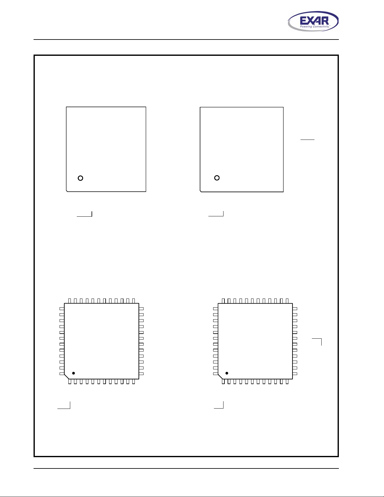
onboard diagnostics. The M580 is available in 32-pin
QFN, 48-pin TQFP and 25-pin BGA packages. All
three packages offer both the 16 mode (Intel bus)
interface and the 68 mode (Motorola bus) interface
which allows easy integration with Motorola
processors.
N
OTE
:
1 Covered by U.S. Patent #5,649,122.
FEATURES
•
Pin-to-pin compatible with XR16L580 in 32-QFN
and 48-TQFP packages
•
Intel or Motorola Bus Interface select
•
16Mbps maximum data rate
•
Selectable TX/RX trigger levels
•
TX/RX FIFO Level Counters
•
Independent TX/RX Baud Rate Generator
•
Fractional Baud Rate Generator
•
Auto RTS/CTS Hardware Flow Control
•
Auto XON/XOFF Software Flow Control
•
Auto RS-485 Half-Duplex Direction Control
•
Multidrop mode w/ Auto Address Detect
•
Sleep Mode with Automatic Wake-up
•
PowerSave mode
•
Infrared (IrDA 1.0 and 1.1) mode
•
1.62V to 3.63V supply operation
•
Crystal oscillator or external clock input
APPLICATIONS
•
Personal Digital Assistants (PDA)
•
Cellular Phones/Data Devices
•
Battery-Operated Devices
•
Global Positioning System (GPS)
•
Bluetooth
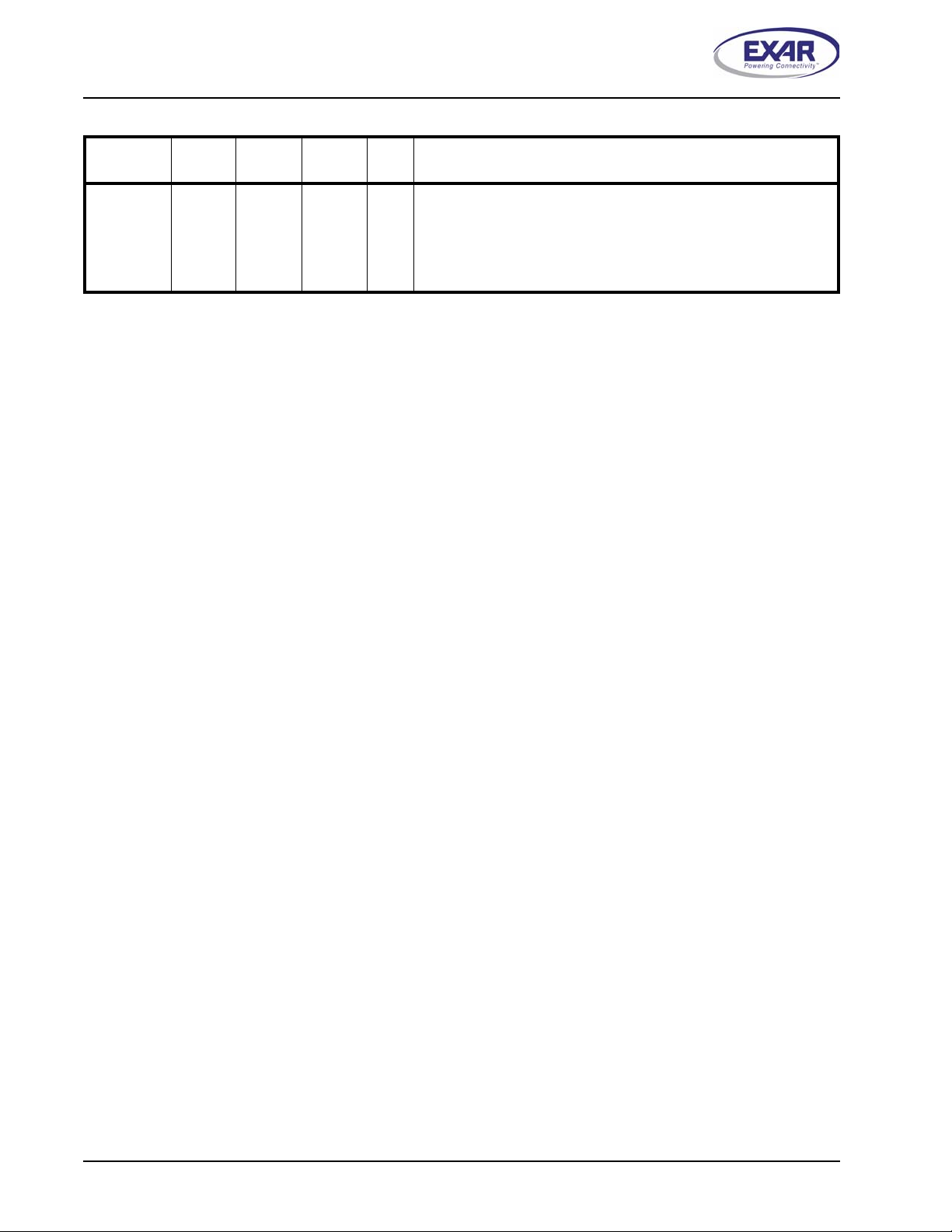
F
IGURE
1. XR16M580 B
PwrSave
A2:A0
D7:D0
IOR#
IOW# (R/W#)
CS#
INT (IRQ #)
RESET
(RESET#)
16/68#
Exar
Corporation 48720 Kato Road, Fremont CA, 94538 • (510) 668-7000 • FAX (510) 668-7017 • www.exar.com
LOCK DIAGRAM
Inte l or
Motorola
Da ta B u s
Inte rfa c e
UART
16 Byte TX FIFO
UART
Regs
BRG
TX &
RX
16 Byte RX FIFO
Cry s ta l O s c /B u ffe r
IR
ENDEC
VCC
(1.62 to 3.63 V)
GND
TX, RX,
RTS#, CTS#,
DTR#, DSR#,
RI#, CD#
XTAL1
XTAL2
XR16M580
1.62V TO 3.63V HIGH PERFORMANCE UART WITH 16-BYTE FIFO
F
IGURE
2. PIN OUT A
CD#
RI#
VCC
D0
D1
D2
D3
25
26
27
28
29
30
31
32
VCC
DSR#
SSIGNMENT FOR
RESET
DTR#
CTS#
24
23
22 21 20 19
32- pin QFN in
Intel Bus Mode
23456
1
D4
D5
16/68#
RTS#
INT
D6
D7RXTX
32-
A0A1A2
18
17
16
15
14
13
12
11
10
78
CS
PIN
9
QFN
NC
NC
#
IOR
GND
#
IOW
2
XTAL
1
XTAL
PwrSave
AND
48-
DSR#
CD#
RI#
VCC
D0
D1
D2
D3
PIN
TQFP P
25
26
27
28
29
30
31
32
GND
CTS#
23 22 21 20 19 18 17
24
23456
1
D4
ACKAGES IN
RESET#
RTS#
IRQ#
DTR#
A0A1A2
32-pin QFN in
Motorola Bus
Mode
D6
D7RXTX
D5
16/68#
16
78
AND
CS#
68 M
16
15
14
13
12
11
10
9
ODE
NC
NC
IOR#
GND
R/W#
XTAL 2
XTAL 1
PwrSave
REV. 1.0.0
VCC
NC
CTS#
DSR#
CD#
RI#
VCC
D0
D1
D2
D3
D4
NC
VCC
RESETNCDTR#
RTS#NCINTNCA0A1A2NCNC
36 35 34 33 32 31 30 29 28 27 26 25
37
38
39
40
41
42
43
44
45
46
47
48
1 2 3 4 5 6 7 8 9 10 11 12
48-TQFP in
Intel Bus Mode
D5D6D7
NC
NC
RX
TX
NC
NC
16/68#
24
23
22
21
20
19
18
17
16
15
14
13
CS#
NC
NC
NC
NC
NC
NC
IOR#
GND
NC
IOW#
XTAL2
XTAL1
PwrSave
NC
CTS#
DSR#
CD#
RI#
VCC
D0
D1
D2
D3
D4
NC
GND
RESET#NCDTR#
NC
36 35 34 33 32 31 30 29 28 27 26 25
37
38
39
40
41
42
43
Motorola Bus Mode
44
45
46
47
48
1 2 3 4 5 6 7 8 9 10 11 12
RTS#NCIRQ#NCA0A1A2
48-TQFP in
D5D6D7
NC
NC
RX
TX
NC
NC
16/68#
NC
NC
24
NC
23
NC
22
21
NC
20
NC
19
IOR#
18
GND
NC
R/W#
XTAL2
XTAL1
PwrSave
VCC
17
16
15
14
13
NC
CS#
2
XR16M580
REV. 1.0.0
F
IGURE
3. PIN OUT A
SSIGNMENT FOR
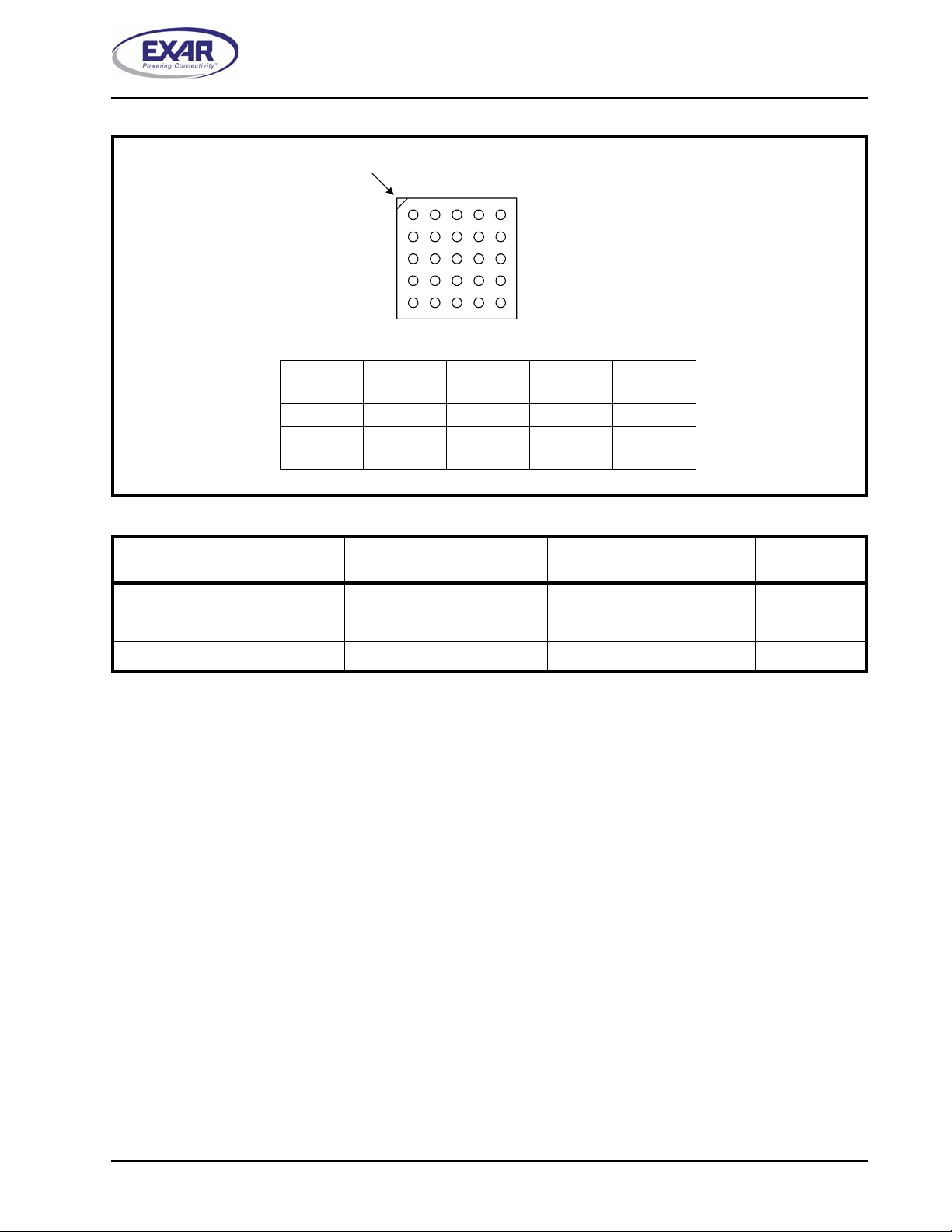
ORDERING INFORMATION
1.62V TO 3.63V HIGH PERFORMANCE UART WITH 16-BYTE FIFO
25-
PIN
BGA P
ACKAGE
A1 Corner
1 2 3 4 5
A
B
C
D
E
Transparent Top View
CTS# RESET INT A1 A2
VCC 16/68# RTS# A0 IOR#
D0 D6 D7 PwrSave IOW#
D3 D1 TX CS# XTAL1
D4 D2 D5 RX GND
O
P
ART NUMBER
XR16M580IL32 32-PinQFN -40°C to +85°C Active
XR16M580IM48 48-Lead TQFP -40°C to +85°C Active
XR16M580IB25 25-Pin BGA -40°C to +85°C Active
P
ACKAGE
PERATING TEMPERATURE
ANGE
R
D
EVICE STATUS
3
XR16M580
1.62V TO 3.63V HIGH PERFORMANCE UART WITH 16-BYTE FIFO
PIN DESCRIPTIONS
Pin Description
N
AME
DA TA BUS INTERFACE
A2
A1
A0
D7
D6
D5
D4
D3
D2
D1
D0
IOR# 14 19 B5 I
IOW#
(R/W#)
CS# 8 11 D4 I
32-QFN
PIN#
48-TQFP
PIN#
17
18
19
5
4
3
1
32
31
30
29
12 16 C5 I
26
27
28
47
46
45
44
43
25-BGA
PIN#
A5
A4
B4
4
3
2
C3
C2
E3
E1
D1
E2
D2
C1
T
YPE
I
Address lines [2:0]. These 3 address lines select the internal registers in UART channel during a data bus transaction.
I/O
Data bus lines [7:0] (bidirectional).
When 16/68# pin is at logic 1, the Intel bus interface is selected and
this input becomes read strobe (active low). The falling edge insti
gates an internal read cycle and retrieves the data byte from an
internal register pointed by the address lines [A2:A0], puts the data
byte on the data bus to allow the host processor to read it on the ris
ing edge.
When 16/68# pin is at logic 0, the Motorola bus interface is selected
and this input should be connected to VCC.
When 16/68# pin is at logic 1, it selects Intel bus interface and this
input becomes write strobe (active low). The falling edge instigates
the internal write cycle and the rising edge transfers the data byte
on the data bus to an internal register pointed by the address lines.
When 16/68# pin is at logic 0, the Motorola bus interface is selected
and this input becomes read (logic 1) and write (logic 0) signal.
This input is chip select (active low) to enable the device.
D
ESCRIPTION
REV. 1.0.0
-
-
INT
(IRQ#)
MODEM OR SERIAL I/O INTERFACE
TX 7 8 D3 O
20 30 A3 O
When 16/68# pin is at logic 1 for Intel bus interface, this output
(OD)
become the active high device interrupt output. The output state is
defined by the user through the software setting of MCR[3]. INT is
set to the active mode when MCR[3] is set to a logic 1. INT is set to
the three state mode when MCR[3] is set to a logic 0. See MCR[3].
When 16/68# pin is at logic 0 for Motorola bus interface, this output
becomes the active low device interrupt output (open drain). An
external pull-up resistor is required for proper operation.
UART Transmit Data or infrared encoder data. S tandard transmit
and receive interface is enabled when MCR[6] = 0. In this mode,
the TX signal will be a logic 1 during reset or idle (no data). Infrared
IrDA transmit and receive interface is enabled when MCR[6] = 1. In
the Infrared mode, the inactive state (no data) for the Infrared
encoder/decoder interface is a logic 0. If it is not used, leave it
unconnected.
4
XR16M580
REV. 1.0.0
Pin Description
N
AME
RX 6 7 E4 I
RTS# 21 32 B3 O
CTS# 24 38 A1 I
DTR# 22 33 - O
DSR# 25 39 - I
CD# 26 40 - I
RI# 27 41 - I
32-QFN
PIN#
48-TQFP
PIN#
25-BGA
PIN#
1.62V TO 3.63V HIGH PERFORMANCE UART WITH 16-BYTE FIFO
YPE
T
UART Receive Data or infrared receive data. Normal receive data
input must idle at logic 1 condition. The infrared receiver idles at
logic 0. This input should be connected to VCC when not used.
UART Request-to-Send (active low) or general purpose output.
This output must be asserted prior to using auto RTS flow control,
see EFR[6], MCR[1] and IER[6].
UART Clear-to-Send (active low) or general purpose input. It can
be used for auto CTS flow control, see EFR[7], MSR[4] and IER[7].
This input should be connected to VCC when not used.
UART Data-Terminal-Ready (active low) or general purpose output.
UART Data-Set-Ready (active low) or general purpose input. This
input should be connected to VCC when not used.
UART Carrier-Detect (active low) or general purpose input. This
input should be connected to VCC when not used.
UART Ring-Indicator (active low) or general purpose input. This
input should be connected to VCC when not used.
D
ESCRIPTION
ANCILLARY SIGNALS
XTAL1 10 14 D5 I
XTAL2 11 15 - O
PwrSave 9 13 C4 I
16/68# 2 1 B2 I
RESET
(RESET#)
VCC 28 42 B1 Pwr
GND 13 18 E5 Pwr
23 35 A2 I
Crystal or external clock input.
Crystal or buffered clock output.
Power-Save (active high). This feature isolates the M580’s data bus
interface from the host preventing other bus activities that cause
higher power drain during sleep mode. See Sleep Mode with Auto
Wake-up and Power-Save Feature section for details. This pin does
not have an internal pull-down resistor. This input should be con
nected to GND when not used.
Intel or Motorola Bus Select. When 16/68# pin is at logic 1, 16 or
Intel Mode, the device will operate in the Intel bus type of interface.
When 16/68# pin is at logic 0, 68 or Motorola mode, the device will
operate in the Motorola bus type of interface. This pin does not
have an internal pull-up or pull-down resistor.
When 16/68# pin is at logic 1 for Intel bus interface, this input
becomes RESET (active high). When 16/68# pin is at logic 0 for
Motorola bus interface, this input becomes RESET# (active low).
A 40 ns minimum active pulse on this pin will reset the internal registers and all outputs of the UART. The UART transmitter output will
be held at logic 1, the receiver input will be ignored and outputs are
reset during reset period (see UART Reset Conditions).
1.62V to 3.63V power supply.
Power supply common, ground.
-
GND Center
Pad
- - Pwr
The center pad on the backside of the QFN package is metallic and
should be connected to GND on the PCB. The thermal pad size on
the PCB should be the approximate size of this center pad and
should be solder mask defined. The solder mask opening should be
at least 0.0025" inwards from the edge of the PCB thermal pad.
5
XR16M580
1.62V TO 3.63V HIGH PERFORMANCE UART WITH 16-BYTE FIFO
REV. 1.0.0
Pin Description
N
AME
NC 15, 16 5, 6, 9,
Pin type: I=Input, O=Output, I/O= Input/output, OD=Output Open Drain.
32-QFN
PIN#
48-TQFP
PIN#
10, 12,
17, 2025, 29,
31, 34,
36, 37, 48
25-BGA
PIN#
-
T
YPE
-
No Connects.
D
ESCRIPTION
1.0 PRODUCT DESCRIPTION
The XR16M580 (M580) is a high performance single channel UART. The configuration registers set is 16550
UART compatible for control, status and data transfer. Additionally, the M580 channel has 16 bytes of transmit
and receive FIFOs, Automatic RTS/CTS Hardware Flow Control, Automatic Xon/Xoff and Special Character
Software Flow Control, infrared encoder and decoder (IrDA ver 1.0 and 1.1), programmable fractional baud
rate generator with a prescaler of divide by 1 or 4, and data rate up to 16 Mbps. The XR16M580 can operate
from 1.62 to 3.63 volts. The M580 is fabricated with an advanced CMOS process.
Data Rate
The M580 is capable of operation up to 16 Mbps at 3.3V with 4X internal sampling clock rate. The device can
operate at 3.3V with a 24 MHz crystal on pins XTAL1 and XT AL2, o r external clo ck source of 32 MHz on XTAL1
pin. With a typical crystal of 1 4.745 6 MHz and thr oug h a software option, the user can set the prescaler bit and
sampling rate for data rates of up to 3.68 Mbps.
Enhanced Features
The rich feature set of the M580 is available through the internal registers. Automatic hardware/software flow
control, selectable transmit and receive FIFO trigger levels, selectable baud rates, infrared encoder/decoder,
modem interface controls, and a sleep mode are all standard features. MCR bit-5 provides a facility for turning
off (Xon) software f low contro l with any incoming (RX) characte r. The M580 includes new features such as 9-bit
(Multidrop) mode, auto RS-485 half-duplex direction control, different baud rate for TX and RX, fast IR mode
and fractional baud rate generator.
6
XR16M580
REV. 1.0.0
1.62V TO 3.63V HIGH PERFORMANCE UART WITH 16-BYTE FIFO
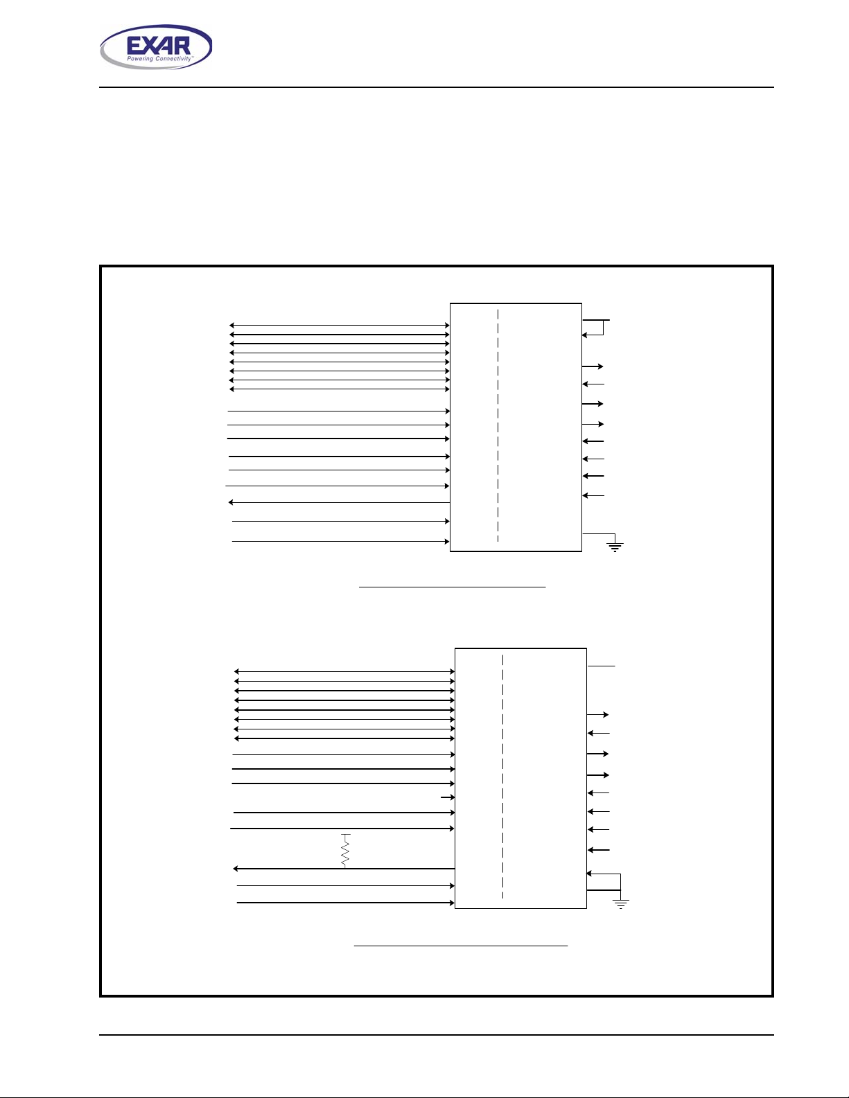
2.0 FUNCTIONAL DESCRIPTIONS
2.1 CPU Interface
The CPU interface is 8 data bits wide with 3 ad dress lines and control signals to execute data bus read and
write transactions. The M580 data interface supports the Intel and motorola compatible types of CPUs. No
clock (oscillator nor external clock) is required for a data bus transaction. Each bus cycle is asynchronous
using CS#, IOR# and IOW# or R/W# inputs. A typical data bus interconnection for Intel and Motorola mode is
shown in
F
IGURE
Figure 4.
4. XR16M580 T
UART_CS#
UART_INT
POWERSAVE
UART_RESET RESET
YPICAL INTEL/MOTOROLA DATA BUS INTERCONNECTIONS
D0
D1
D2
D3
D4
D5
D6
D7
A0
A1
A2
IOR#
IOW #
D0
D1
D2
D3
D4
D5
D6
D7
A0
A1
A2
IOR#
IOW#
CS#
INT
PwrSave
16/68#
TX
RX
DTR#
RTS#
CTS#
DSR#
CD#
RI#
GND
VCCVCC
Serial Transceivers of
RS-232
RS-485
RS-422
Or Infrared
Intel Data Bus Interconnections
D0
D1
D2
D3
D4
D5
D6
D7
A0
A1
A2
R/W#
UART_CS#
UART_IRQ#
POWERSAVE
UART_RESET# RESET
vcc
NC
D0
D1
D2
D3
D4
D5
D6
D7
A0
A1
A2
IOR #
IOW #
CS#
INT
PwrSave
Motorola Data Bus Interconnections
DTR#
RTS#
CTS#
DSR#
CD#
RI#
16/68#
GND
TX
RX
VCCVCC
Serial Transceivers of
RS-232
RS-485
RS-422
Or Infrared
7
XR16M580
1.62V TO 3.63V HIGH PERFORMANCE UART WITH 16-BYTE FIFO
REV. 1.0.0
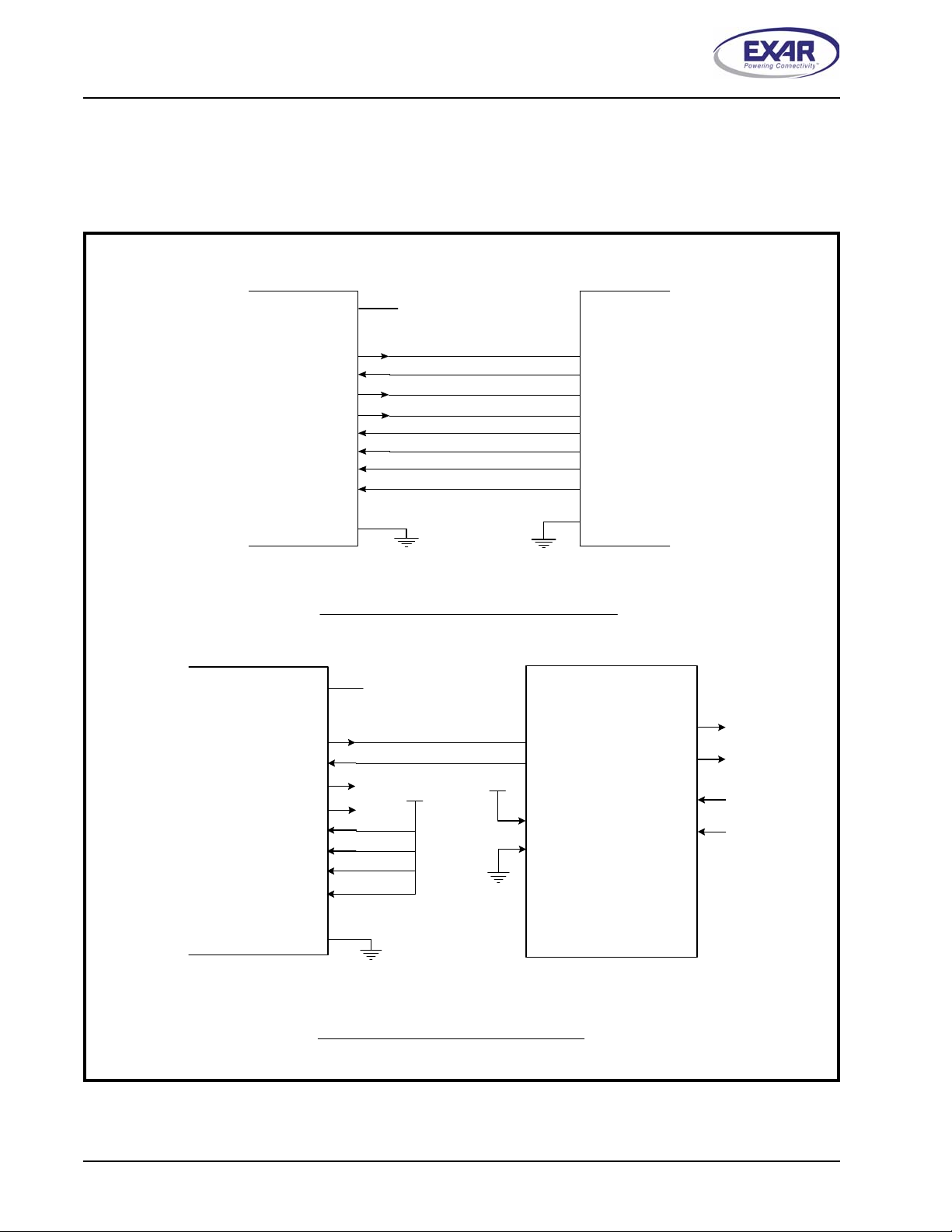
2.2 Serial Interface
The M580 is typically used with RS-232, RS-485 and IR transceivers. The following figure shows typical
connections from the UART to the different transceivers. For more information on RS-232 and RS-485/422
transceivers, go to www.exar.com or send an e-mail to uarttechsupport@exar.com.
F
IGURE
5. XR16M580 T
YPICAL SERIAL INTERFACE CONNECTIONS
VCCVCC
TX
RX
DTR#
UART
RTS#
CTS#
DSR#
CD#
RI#
GND
RS -232
Transceiver
T1IN
R1OUT
T2IN
T3IN
R2OUT
R3OUT
R4OUT
R5OUT
GND
UART
R S-23 2 Fu ll -Modem S e r ia l In terfa c e
NC
NC
VCC
DI
RO
VCC
VCC
DE
RE#
VCC
TX
RX
RTS#
DTR#
CTS#
DSR#
CD
RI
GND
#
#
RS-485 Full-Duplex Serial Interface
RS-485
Transceiver
Full-duplex
TX+
TX-
RX+
RX-
8

XR16M580
REV. 1.0.0
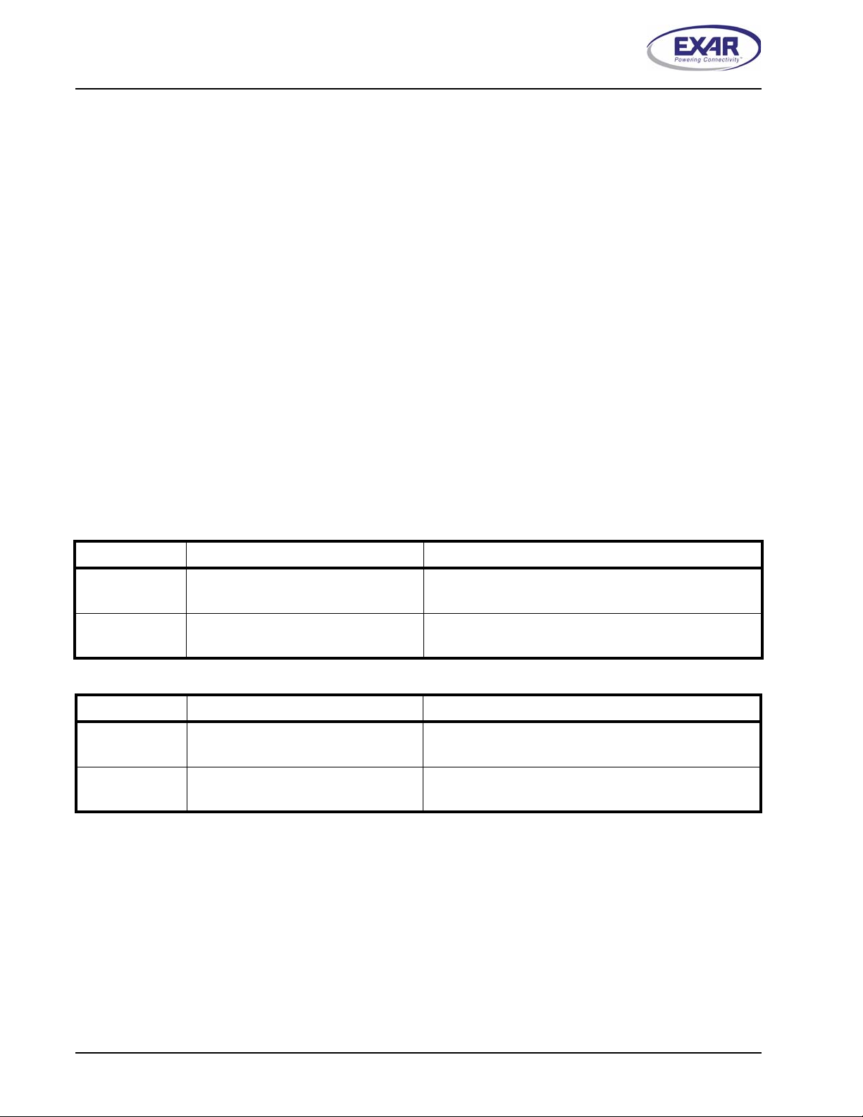
F
IGURE
6. XR16M580 T
1.62V TO 3.63V HIGH PERFORMANCE UART WITH 16-BYTE FIFO
YPICAL SERIAL INTERFACE CONNECTIONS
VCC
NC
VCC
RS-485 Half-Duplex Serial Interface
UART
VCC
TX
RX
RTS#
DTR#
CTS#
DSR#
CD
RI
GND
#
#
DI
RO
DE
RE#
RS-485
Transceiver
Half-duplex
Y
Z
A
B
UART
TX
RX
DTR#
RTS#
CTS#
DSR#
CD#
RI#
GND
VCCVCC
NC
NC
VCC
Infrared Connection
IR
Transceiver
TXD
RXD
9
XR16M580
1.62V TO 3.63V HIGH PERFORMANCE UART WITH 16-BYTE FIFO
REV. 1.0.0
2.3 Device Reset
The RESET input resets the internal registers and the serial interface outputs to their default state (see
Table 16). An active high pulse of longer than 40 ns duration will be required to activate the reset function in
the device. Following a power-on reset or an external reset, the M580 is software compatible with previous
generation of UARTs, XR16L580 and ST16C550.
2.4 Internal Registers
The M580 has a set of 16550 compatible registers for controlling, monitoring and data loading and unloading.
These registers function as data holding registers (THR/RHR), interrupt status and control registers (ISR/IER),
a FIFO control register (FCR), receive line status and control registers (LSR/LCR), modem status and control
registers (MSR/MCR), programmable dat a rate (clock) divisor registers (DL L/DLM/DLD), and a u ser accessibl e
scratchpad register (SPR).
Beyond the general 16C550 features an d cap abiliti es, the M580 offers enhanced feature registers (EFR, Xon1/
Xoff 1, Xon2/Xoff 2, DLD, FCTR, EMSR and FC) that provide automatic RTS and CTS hardware flow control,
automatic Xon/Xoff software flow control, 9-bit (Multidrop) mode, auto RS-485 half duplex control, different
baud rate for TX and RX and fractional baud rate generator. All the registe r functions are discussed in full
detail later in
“Section 3.0, UART INTERNAL REGISTERS” on page 24.
2.5 INT Ouput
The interrupt outputs change according to the operating mode and enhanced features setup. Table 1 and 2
summarize the operating behavior for the transmitter and receiver. Also see Figure 22 through 25.
N
OTE
: The IRQ# pin requires a pull-up resistor for proper operation.
INT Pin
(16/68# = 1)
IRQ# Pin
(16/68# = 0)
INT Pin
(16/68# = 1)
IRQ# Pin
(16/68# = 0)
T
ABLE
1: INT PIN O
FCR BIT-0 = 0 (FIFO D
LOW = One byte in THR
HIGH = THR empty
HIGH = One byte in THR
LOW = THR empty
T
ABLE
FCR BIT-0 = 0 (FIFO D
HIGH = One byte in RHR
LOW = RHR empty
LOW = One byte in RHR
HIGH = RHR empty
ISABLED
) FCR BIT-0 = 1 (FIFO E
2: INT PIN O
ISABLED
) FCR BIT-0 = 1 (FIFO E
PERATION FOR TRANSMITTER
NABLED
LOW = FIFO above trigger level
HIGH = FIFO below trigger level or FIFO empty
HIGH = FIFO above trigger level
LOW = FIFO below trigger level or FIFO empty
PERATION FOR RECEIVER
NABLED
LOW = FIFO below trigger level
HIGH = FIFO above trigger level or RX Data Timeout
HIGH = FIFO below trigger level
LOW = FIFO above trigger level or RX Data Timeout
)
)
10
XR16M580
REV. 1.0.0
1.62V TO 3.63V HIGH PERFORMANCE UART WITH 16-BYTE FIFO
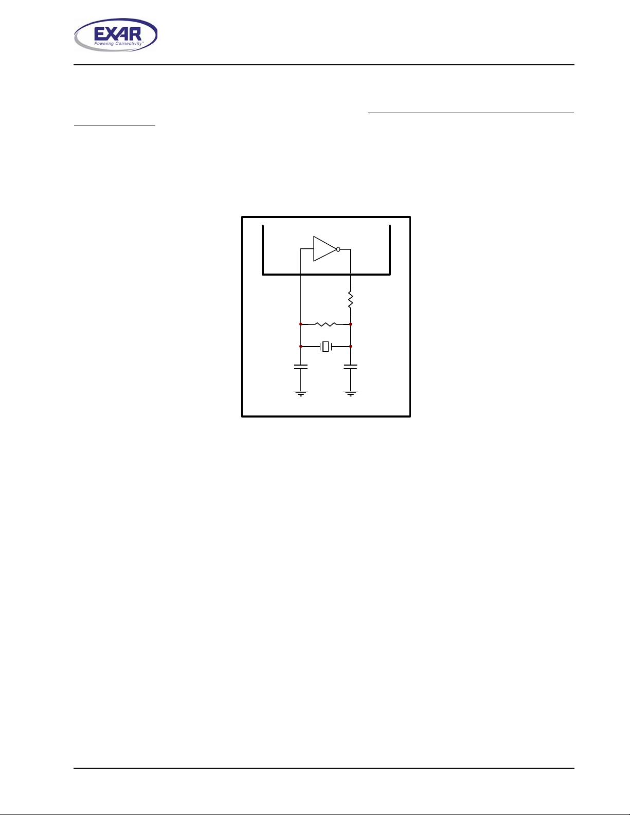
2.6 Crystal Oscillator or External Clock Input
The M580 includes an on-c hip oscillat or to produce a clock for the baud rate generators in the device when a
crystal is connected between XTAL1 and XTAL2 as show belo w.
The CPU data bus does not require this clock
for bus operation. The crystal oscillator provides a system clock to the Baud Rate Generators (BRGs) in the
UART. XTAL1 is the input to the oscillator or external clock buffer input with XTAL2 pin being the output. For
programming details, see
“Section 2.7, Programmable Baud Rate Generator with Fractional Divisor” on
page 12.
F
IGURE
7. T
YPICAL CRYSTAL CONNECTIONS
XTAL1 XTAL2
R2
500K - 1M
C1
22-47pF
22-47pF
Y1
C2
R1
0-120
(O p tional)
1.8432 MHz
to
24 MHz
The on-chip oscillator is designed to use an industry standard microprocessor crystal (parallel resonant,
fundamental frequency with 10-22 pF capacitance load, ESR of 20-120 ohms and 100ppm frequency
tolerance) connected externally between the XTAL1 and XTAL2 pins. Typical oscillator connections are shown
in
Figure 7. Alternatively, an external clock can be connected to the XTAL1 pin to clock the internal baud rate
generator for standard or custom rates. The BGA package has XTAL1 only, the external clock is required. For
further reading on oscillator circuit, see application note DAN108 on EXAR’s web site.
11
XR16M580
1.62V TO 3.63V HIGH PERFORMANCE UART WITH 16-BYTE FIFO
REV. 1.0.0
2.7 Programmable Baud Rate Generator with Fractional Divisor
The M580 has independent Baud Rate Generators (BRGs) with prescalers for the transmitter and receiver.
The prescaler is controlled by a software bit in the MCR register. The MCR register bit-7 sets the prescaler to
divide the input crystal or external clock by 1 or 4. The output of the prescaler clocks to the BRG. The BRG
further divides this clock by a programmable divisor between 1 and (2
16
- 0.0625) in increments of 0.0625 (1/
16) to obtain a 16X or 8X or 4X sampling clock of the serial data rate. The sampling clock is used by the
transmitter for data bit shifting and receiver for data sampling. For transmitter and receiver, the M580 provides
respective BRG divisors. The BRG divisor (DLL, DLM, and DLD registers) defaults to the value of ’1’ (DLL =
0x01, DLM = 0x00 and DLD = 0x00) upon re se t. Ther ef or e, the BRG mu st be pr ogra m me d du ring in itia liza tion
to the operating data rate. The DLL and DLM registers provide the integer part of the divisor and the DLD
registers provides the fractional part of the divisor. The four lower bits of the DLD are used to select a value
from 0 (for setting 0000) to 0.9375 or 15/16 (for setting 1111). Programming the Baud Rate Generator
Registers DLL, DLM and DLD provide s the capability for selecting the operating da ta rate.
Table 3 shows the
standard data rates available with a 24MHz crystal or external clock at 16X clock rate. If the pre-scaler is used
(MCR bit-7 = 1), the output data rate will be 4 time s less than that shown in
Table 3. At 8X sampling rate, these
data rates would double. And at 4X sampling rate, they would quadruple. Also, when using 8X sampling mode,
please note that the bit-time will have a jitter (+/- 1/16) whenever the DLD is non-zero and is an odd number.
When using a non-standard data rate crystal or external clock, the divisor value can be calculated with the
following equation(s):
Required Divisor (decimal)=(XTAL1 clock frequency / prescaler) /(serial data rate x 16), with 16X mode,
DLD[5:4]=’00’
Required Divisor (decimal)= (XTAL1 clock frequency / prescaler / (serial data rate x 8), with 8X mode,
Required Divisor (decimal)= (XTAL1 clock frequency / prescaler / (serial data rate x 4), with 4X mode,
DLD[5:4] = ’01’
DLD[5:4] = ’10’
The closest divisor that is obtainable in the M580 can be calculated using the following formula:
ROUND( (Required Divisor - TRUNC(Required Divisor) )*16)/16 + TRUNC(Required Divisor), where
DLM = TRUNC(Required Divisor) >> 8
DLL = TRUNC(Required Divisor) & 0xFF
DLD = ROUND( (Required Divisor-TRUNC(Required Divisor) )*16)
In the formulas above, please note that:
TRUNC (N) = Integer Part of N. For example, TRUNC (5.6) = 5.
ROUND (N) = N rounded towards the closest integer. For example, ROUND (7.3) = 7 and ROUND (9.9) = 10.
A >> B indicates right shifting the value ’A’ by ’B’ number of bits. For example, 0x78A3 >> 8 = 0x0078.
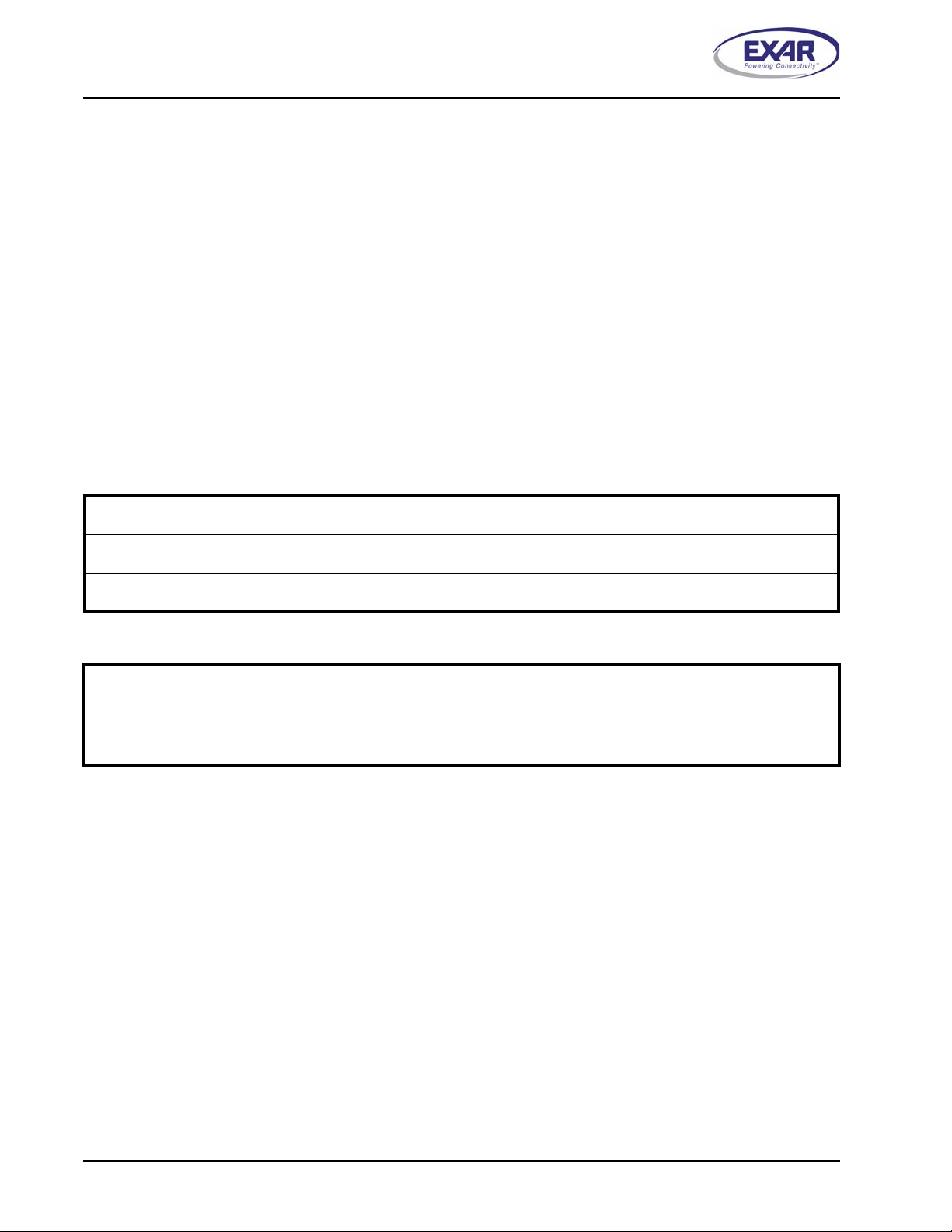
2.7.1 Independent TX/RX BRG
The XR16M580 has two independent set s of TX and RX ba ud rate ge nerator. Please see the Figure 8. TX and
RX can work in different baud rate by setting DLD, DLL and DLM register. For example, TX can transmit data
to the remote UART at 9600 bps while RX receives data from remote UART at 921.6 Kbps. For the baud rate
setting, please
See ”Section 4.13, Baud Rate Generator Registers (DLL, DLM and DLD) - Read/Write” on
page 38..
12
XR16M580
REV. 1.0.0
F
IGURE
8. B
XTAL1
XTAL2
Required
Output Data
Rate
AUD RATE GENERATOR
Crystal
Osc
/
Buffer
T
ABLE
3: T
YPICAL DATA RATES WITH A
D
IVISOR FOR
Clock
(Decimal)
Prescaler
Divide by 1
Prescaler
Divide by 4
16x
1.62V TO 3.63V HIGH PERFORMANCE UART WITH 16-BYTE FIFO
MCR Bit 7=0
(default)
MCR Bit-7=1
D
IVISOR
BTAINABLE IN
O
M580
DLD[7]=0
-
DLD[7]=1
24 MHZ
DLM P
DLL
DLM
DLD[5:0]
DLL
DLM
DLD[5:0]
CRYSTAL OR EXTERNAL CLOCK AT
ALUE
V
ROGRAM
(HEX)
DLL P
V
ALUE
DLD[6]
ROGRAM
(HEX)
0
1
DLD P
ALUE
V
16X or 8X or 4X
Sampling Rate Clock
16X or 8X or 4X
Sampling Rate Clock
16X S
ROGRAM
(HEX)
400 3750 3750 E A6 0 0
2400 625 625 2 71 0 0
4800 312.5 312 8/16 1 38 8 0
9600 156.25 156 4/16 0 9C 4 0
10000 150 150 0 96 0 0
19200 78.125 78 2/16 0 4E 2 0
25000 60 60 0 3C 0 0
28800 52.0833 52 1/16 0 34 1 0.04
38400 39.0625 39 1/16 0 27 1 0
50000 30 30 0 1E 0 0
57600 26.0417 26 1/16 0 1A 1 0.08
75000 20 20 0 14 0 0
100000 15 15 0 F 0 0
115200 13.0208 13 0 D 0 0.16
153600 9.7656 9 12/16 0 9 C 0.16
200000 7.5 7 8/16 0 7 8 0
225000 6.6667 6 11/16 0 6 B 0.31
230400 6.5104 6 8/16 0 6 8 0.16
250000 6 6 0 6 0 0
300000 5 5 0 5 0 0
400000 3.75 3 12/16 0 3 C 0
460800 3.2552 3 4/16 0 3 4 0.16
500000 3 3 0 3 0 0
750000 2 2 0 2 0 0
921600 1.6276 1 10/16 0 1 A 0.16
1000000 1.5 1 8/16 0 1 8 0
to Transmitter
to Receiver
AMPLING
D
ATA ERROR
ATE
R
(%)
13
XR16M580
1.62V TO 3.63V HIGH PERFORMANCE UART WITH 16-BYTE FIFO
REV. 1.0.0
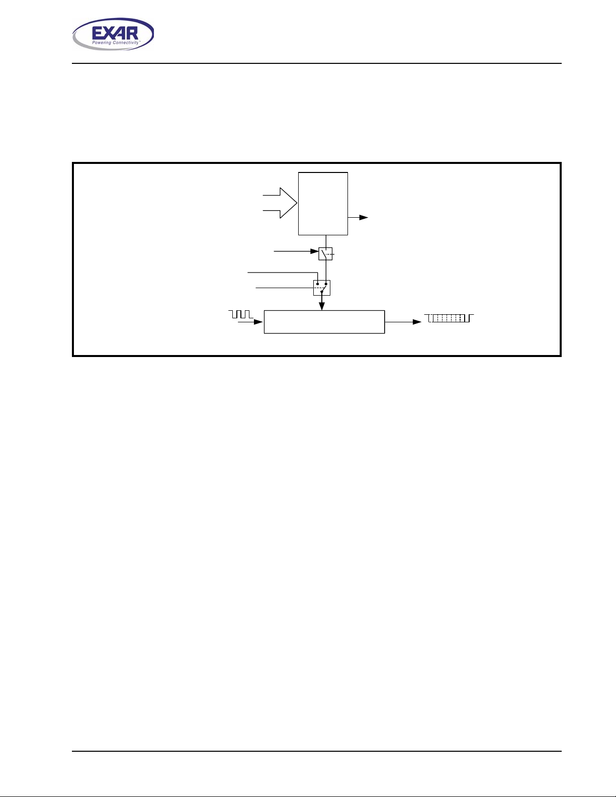
2.8 Transmitter
The transmitter section comprises of an 8-bit Transmit Shift Register (TSR) and 16 bytes of FIFO which
includes a byte-wide Transmit Holding Register (THR). TSR shifts out every data bit with the 16X/8X/4X
internal clock. A bit time is 16/8/4 clock periods. The transmitter sends the start-bit followed by the number of
data bits, inserts the proper parity-bit if enabled, and adds the stop-bit(s). The status of the FIFO and TSR are
reported in the Line Status Register (LSR bit-5 and bit-6).
2.8.1 Transmit Holding Register (THR) - Write Only
The transmit holding register is an 8-bit register providing a data interface to the host processor. The host
writes transmit data byte to the THR to be converted into a serial data stream including start-bit, data bits,
parity-bit and stop-bit(s). The least-significant-bit (Bit-0) becomes first data bit to go out. The THR is the input
register to the transmit FIFO of 16 bytes when FIFO operation is enabled by FCR bit-0. Every time a write
operation is made to the THR, the FIFO data pointer is automatically bumped to the next sequential data
location.
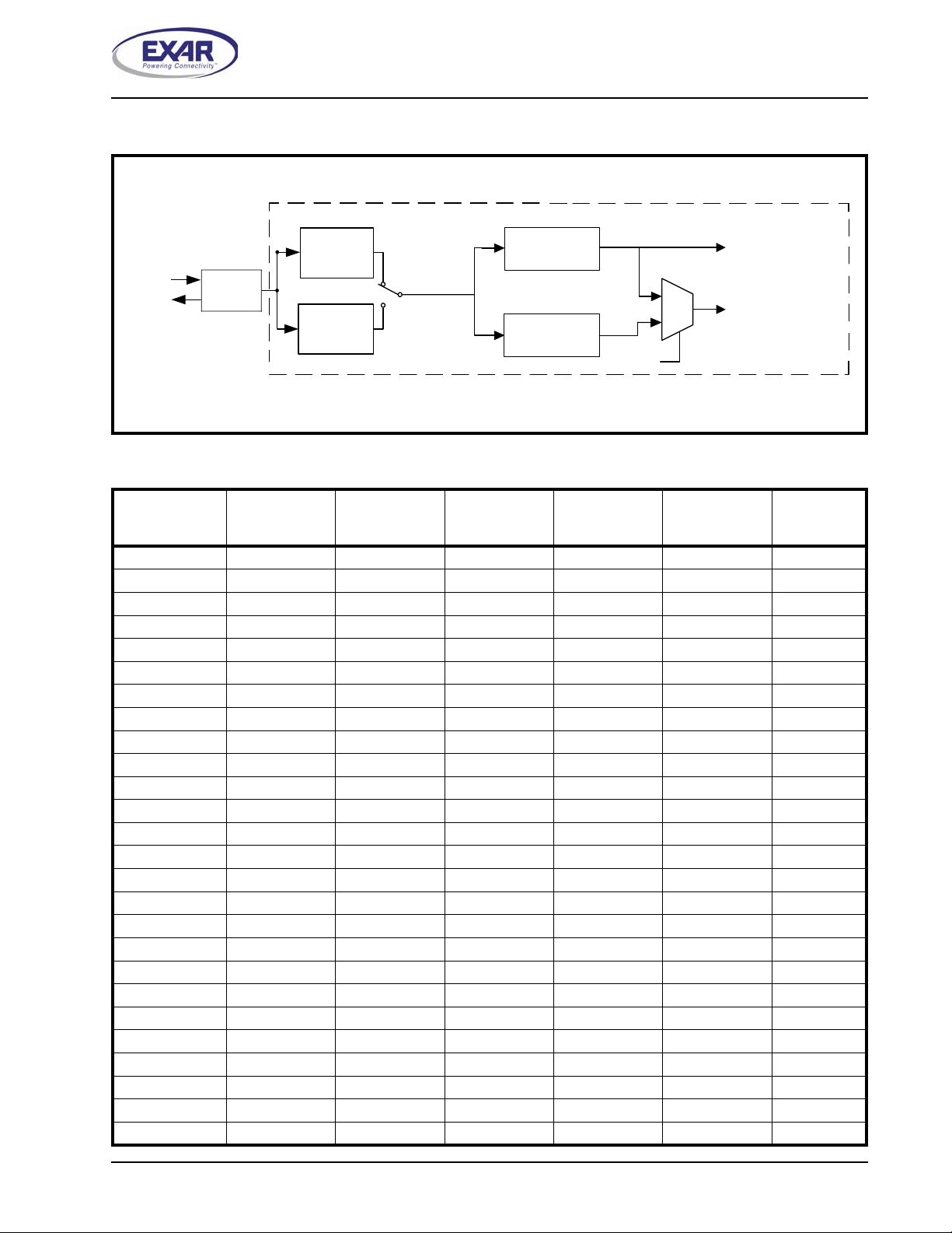
2.8.2 Transmitter Operation in non-FIFO Mode
The host loads transmit data to THR one character at a time. The THR empty flag (LSR bit-5) is set when the
data byte is transferred to TSR. THR fl ag can ge nerate a tr ansmit emp ty inter rupt (ISR bit -1) when it is enable d
by IER bit-1. The TSR flag (LSR bit-6) is set when TSR becomes completely empty.
F
IGURE
9. T
RANSMITTER OPERATION IN NON
-FIFO M
ODE
Data
Byte
16X or 8X or 4X
Clock
( DLD[5:4] )
Transmit
Holding
Register
(THR)
Transmit Shift Register (TSR)
THR Interrupt (ISR bit-1)
Enabled by IER bit-1
M
S
B
L
S
B
TXNOFIFO1
14
XR16M580
REV. 1.0.0
1.62V TO 3.63V HIGH PERFORMANCE UART WITH 16-BYTE FIFO
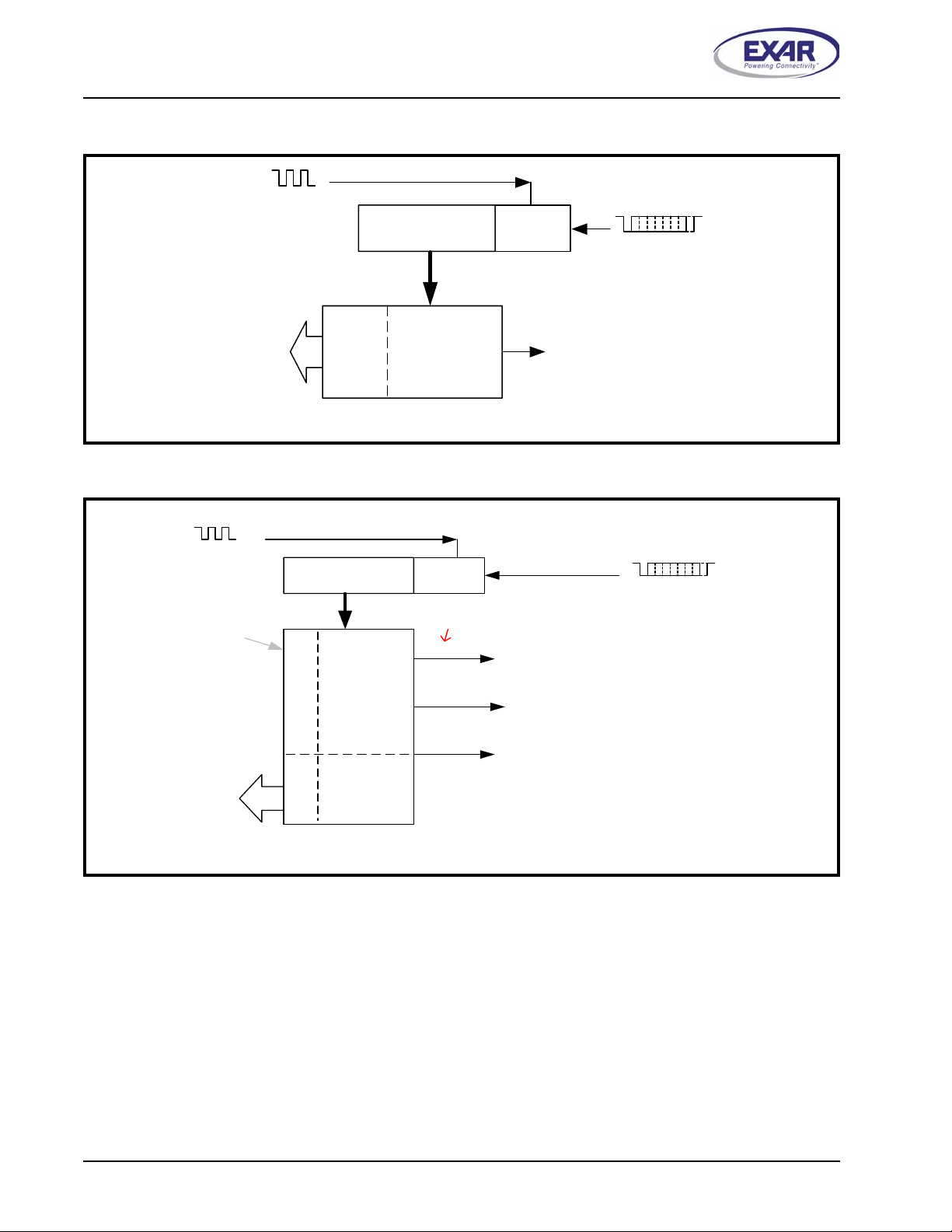
2.8.3 Transmitter Operation in FIFO Mode
The host may fill the transmit FIFO with up to 16 bytes of transmit data. The THR empty flag (LSR bit-5) is set
whenever the FIFO is empty. The THR empty flag can generate a transmit empty interrupt (ISR bit-1) when th e
FIFO becomes empty. The transmit empty interrupt is enabled by IER bit-1. The TSR flag (LSR bit-6) is set
when TSR/FIFO becomes empty.
F
IGURE
10. T
RANSMITTER OPERATION IN
Auto CTS Flow Control (CTS# pin)
Flow Control Characters
(Xoff1/2 and Xon1/2 Reg.)
Auto Software Flow Con tr ol
16X or 8X or 4X Clock
(DLD[5 :4 ])
FIFO
Transmit
Data Byte
AND FLOW CONTROL MODE
Transmit
FIFO
Transmit Data Shift Register
(TSR)
THR Inte rr u p t (ISR b it-1 ) fa lls
below the programmed Trigger
Level and then when becomes
empty. FIFO is Enabled by FCR
bit-0=1
TXFIFO1
2.9 Receiver
The receiver section contains an 8-bit Receive Shift Register (RSR) and 16 bytes of FIFO which includes a
byte-wide Receive Holding Register (RHR). The RSR uses the 16X/8X/4X clock (DLD[5:4]) for timing. It
verifies and validates every bit on the incoming character in the middle of each data bit. On th e falling edge o f
a start or false start bit, an internal receiver counter starts counting a t the 16X/8X/4X clock rate . After 8 clocks
(or 4 if 8X or 2 if 4X) the start bit period should be at the center of the start bit. At this time the start bit is
sampled and if it is still a logic 0 it is validated. Evaluating the st ar t bit in t his manner p revent s t he receiver f rom
assembling a false character. The rest of the data bits and st op bits are sampled and validated in t his same
manner to prevent false framing. If t here we re any er ror( s), t hey are rep orted in th e LSR regist er bit s 2-4. Upon
unloading the receive data byte from RHR, the receive FIFO pointer is bumped and the error tags are
immediately updated to reflect the status of the data byte in RHR register. RHR can generate a receive data
ready interrupt upon receiving a character or delay until it reaches the FIFO trigger level. Furthermore, data
delivery to the host is guaranteed by a receive data ready time-out interrupt when data is not received for 4
word lengths as defined by LCR[1:0] plus 12 bits time. This is equivalent to 3.7-4.6 character times. The RHR
interrupt is enabled by IER bit-0. See
Figure 11 and Figure 12 below.
2.9.1 Receive Holding Register (RHR) - Read-Only
The Receive Holding Register is an 8-bit register that holds a receive data byte from the Receive Shift
Register. It provides the receive data interface to the host processor. The RHR register is part of the receive
FIFO of 16 bytes by 11-bits wide, the 3 extra bits are for the 3 error tags to be reported in LSR regis ter. When
the FIFO is enabled by FCR bit-0, the RHR contains the first data character received by the FIFO. After the
RHR is read, the next character byte is loaded into the RHR and the errors associated with the current data
byte are immediately updated in the LSR bits 2-4.
15
XR16M580
1.62V TO 3.63V HIGH PERFORMANCE UART WITH 16-BYTE FIFO
F
IGURE
11. R
F
IGURE
ECEIVER OPERATION IN NON
16X or 8X or 4X Clock
( DLD[5:4] )
Receive
Data By te
and Errors
12. R
ECEIVER OPERATION IN
-FIFO M
Receive Data Shift
Error
Tags in
LSR bits
4:2
FIFO
AND AUTO
ODE
Register (RSR)
Receive Data
Holding Register
(RHR)
RTS F
Data Bit
Validation
LOW CONTROL MODE
REV. 1.0.0
Receive Data Characters
RHR Inte rrup t (IS R b it-2)
RXFIFO1
16X or 8X or 4X Clock
( DLD[5:4] )
16 bytes by 11-bit w ide
Receive Data
By te a n d E rrors
FIFO
Receive Data Shift
Register (RSR)
Receive
Da ta F IF O
(16-sets)
Error Tags
Receive
Data
LSR bits 4:2
Error Tags in
Da ta B it
Va lida tion
Example
- RX FIFO trigger level selected at 8 bytes
:
Da ta fa l ls to
4
FIFO
Trigger=8
Data fills to
14
(See Note Below)
RTS# re - a s s e rts wh e n da ta falls b elow th e flo w
con tr o l trig ger le v e l to r e s ta r t re mo te tr a nsmitte r.
Enable by EFR bit-6=1, MCR bit-1.
RHR Interrupt (ISR bit-2) programmed for
desired FIF O trigger level.
FIFO is Enabled by FCR bit-0=1
RTS# de-asserts when data fills above the flow
control trigger level to suspend remote transmitter.
Enable by EFR bit-6=1, MCR bit-1.
Receive Data Characters
RXFIFO1
16
XR16M580
REV. 1.0.0
1.62V TO 3.63V HIGH PERFORMANCE UART WITH 16-BYTE FIFO
2.10 Auto RTS (Hardware) Flow Control
Automatic RTS hardware flow control is used to prevent data overrun to the local receiver FIFO. The RTS#
output is used to request remote unit to suspend/resume data transmission. The auto RTS flow control
features is enabled to fit specific application requir em e nt (see
•
Enable auto RTS flow control using EFR bit-6.
•
The auto RTS function must be started by assert ing RTS# out put pin (MCR bit-1 to logic 1 af ter it is enabled).
Figure 13):
If using the Auto RTS interrupt:
•
Enable RTS interrupt through IER bit-6 (after setting EFR bit-4). The UART issues an interrupt when the
RTS# pin makes a transition from low to high: ISR bit-5 will be set to logic 1.
2.11 Auto RTS Hysteresis
With the Auto RTS function enabled, an interr upt is gen erated when the receive FI FO reaches the select ed RX
trigger level. The RTS# pin will not be forced HIGH (RTS off) until the receive FIFO reaches one trigger level
above the selected trigger level in the trigger table (
Table 9). The RTS# pin will return LOW after the RX FIFO
is unloaded to one level below the selected trigger level. Under the above described conditions, the M580 will
continue to accept data until the receive FIFO gets full. The Auto RTS function is initiated when the RTS#
output pin is asserted LOW (RTS On).
T
ABLE
4: A
UTO
RX T
RIGGER LEVEL
INT PIN A
RTS (H
CTIVATION
ARDWARE
) F
RTS# DE-
(C
HARACTERS IN RX FIFO
LOW CONTROL
ASSERTED
(H
IGH
)
RTS# A
)
(C
SSERTED
HARACTERS IN RX FIFO
(LOW)
)
1 1 4 0
4 4 8 1
8 8 14 8
14 14 14 14
2.12 Auto CTS Flow Control
Automatic CTS flow control is used to prevent data overrun to the remot e receiver FIFO. The CTS# input is
monitored to suspend/restart the local transmitter. The auto CTS flow control feature is selected to fit specific
application requirement (see
•
Enable auto CTS flow control using EFR bit-7.
Figure 13):
If needed, the CTS interrupt can be enabled through IER bit-7 (after setting EFR bit-4). The UART issues an
interrupt when the CTS# pin is de-asserted (HIGH): ISR bit-5 will be set to 1, and UART will suspend
17
 Loading...