

EXAR XR16M2650 Service Manual

查询XR16M2650IL32供应商
XR16M2650
HIGH PERFORMANCE LOW VOLTAGE DUART WITH 32-BYTE FIFO
MAY 2007 REV. 1.0.2
GENERAL DESCRIPTION
The XR16M26501 (M2650) is a high performance
dual universal asynchronous receiver and transmitter
(UART) with 32 bytes TX and RX FIFOs. The device
operates from 1.62 to 3.63 volts and is pin-to-pin and
software compatible to the ST16C2550, XR16V2550
and XR16V2650. It supports Exar’s enhanced
features of selectable FIFO trigger level, automatic
hardware (RTS/CTS) and software flow control, and a
complete modem interface. Onboard registers
provide the user with operational status and data
error flags. An internal loopback capability allows
system diagnostics. Independent programmable
baud rate generators are provided in each channel to
select data rates up to 16 Mbps at 3.3 Volt with 4X
sampling clock. The M2650 is available in 48-pin
TQFP and 32-pin QFN packages.
NOTE: 1 Covered by U.S. Patent #5,649,122
APPLICATIONS
• Portable Appliances
• Telecommunication Network Routers
• Ethernet Network Routers
• Cellular Data Devices
• Factory Automation and Process Controls
FEATURES
• 1.62 to 3.63 Volt Operation
• Pin-to-pin and software compatible to ST16C2550
in the 48-TQFP package
• Pin-to-pin and software compatible to XR16L2550,
XR16V2550 and XR16V2650
• Two independent UART channels
■ Register set is 16550 compatible
■ Data rate of up to 16 Mbps at 3.3 V
■ Data rate of up to 12.5 Mbps at 2.5 V
■ Data rate of up to 8 Mbps at 1.8V
■ Fractional Baud Rate Generator
■ Transmit and Receive FIFOs of 32 bytes
■ Selectable TX and RX FIFO Trigger Levels
■ Automatic Hardware (RTS/CTS) Flow Control
■ Automatic Software (Xon/Xoff) Flow Control
■ Wireless Infrared (IrDA 1.0) Encoder/Decoder
■ Automatic sleep mode
■ Full modem interface
• Device Identification and Revision
• Crystal oscillator (up to 24MHz) or external clock
(up to 64MHz) input
• 48-TQFP and 32-QFN packages
FIGURE 1. XR16M2650 BLOCK DIAGRAM
A2:A0
D7:D0
IOR#
IOW#
CSA#
CSB#
INTA
INTB
TXRDYA#
TXRDYB#
RXRDYA#
RXRDYB#
Reset
8-bit Data
Bus
Interface
UART Channel A
UART
Regs
BRG
32 Byte TX FIFO
TX & RX
32 Byte RX FIFO
UART Channel B
(same as Channel A)
Crystal Osc/Buffer
IR
ENDEC
1.62 to 3.63 Volt VCC
GND
TXA, RXA, DTRA#,
DSRA#, RTSA#,
CTSA#, CDA#, RIA#,
OP2A#
TXB, RXB, DTRB#,
DSRB#, RTSB#,
CTSB#, CDB#, RIB#,
OP2B#
XTAL1
XTAL2
Exar Corporation 48720 Kato Road, Fremont CA, 94538 • (510) 668-7000 • FAX (510) 668-7017 • www.exar.com
XR16M2650
HIGH PERFORMANCE LOW VOLTAGE DUART WITH 32-BYTE FIFO REV. 1.0.2
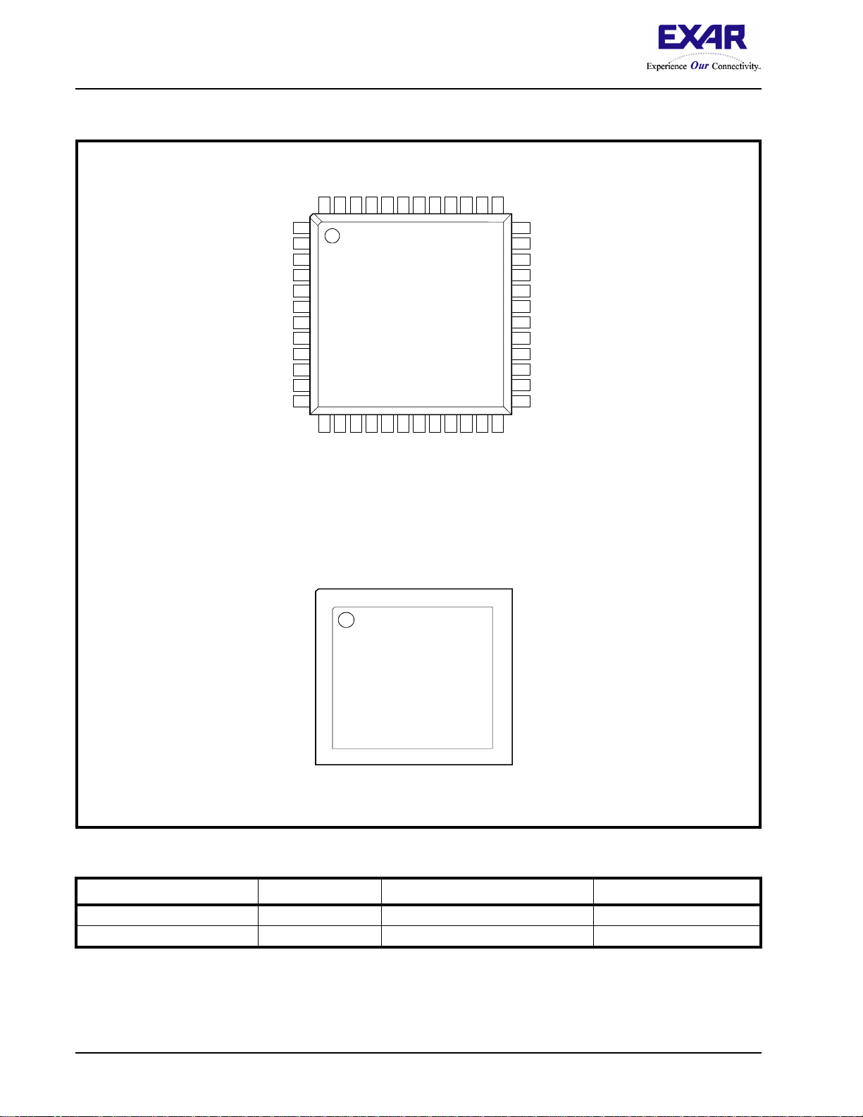
FIGURE 2. PIN OUT ASSIGNMENT
D5
D6
D7
RXB
RXA
TXRDYB#
TXA
TXB
OP2B#
CSA#
CSB#
NC
7
8
9
10
11
12
D6
D7
RXB
RXA
TXA
TXB
CSA#
CSB#
D4
D3
D2D1D0
48
47
464544
1
2
3
4
5
6
15
13
14
IOW#
XTAL2
XTAL1
D5
32
TXRDYA#
434241
XR16M2650
48-pin TQFP
1819202122
16
17
GND
CDB#
RXRDYB#
D4D3D2
31
30
29
1
2
3
4
5
XR16M2650
32-pin QFN
6
7
8
9
11
12
10
RIA#
VCC
IOR#
DSRB#
D1
28
13
CDA#
DSRA#
40
39
RIB#
RTSB#
VCC
D0
272625
14
15
CTSA#
16
CTSA#
38
23
CTSB#
NC
24
23
22
21
20
19
18
17
NC
37
RESET
36
DTRB#
35
DTRA#
34
RTSA#
33
OP2A#
32
RXRDYA#
31
INTA
30
INTB
29
A0
28
A1
27
A2
26
NC
25
24
RESET
RTSA#
INTA
INTB
A0
A1
A2
NC
NC
XTAL1
GND
IOR#
IOW#
XTAL2
RTSB#
CTSB#
ORDERING INFORMATION
PART NUMBER PACKAGE OPERATING TEMPERATURE RANGE DEVICE STATUS
XR16M2650IL32 32-Pin QFN -40°C to +85°C Active
XR16M2650IM48 48-Lead TQFP -40°C to +85°C Active
2
XR16M2650
REV. 1.0.2 HIGH PERFORMANCE LOW VOLTAGE DUART WITH 32-BYTE FIFO
PIN DESCRIPTIONS
Pin Description
NAME
DATA BUS INTERFACE
A2
A1
A0
D7
D6
D5
D4
D3
D2
D1
D0
IOR# 14 19 I
IOW# 12 15 I
CSA# 7 10 I
CSB# 8 11 I
INTA 22 30 O
INTB 21 29 O
TXRDYA# - 43 O
32-QFN
PIN #
18
19
20
2
1
32
31
30
29
28
27
48-TQFP
PIN #
26
27
28
3
2
1
48
47
46
45
44
TYPE DESCRIPTION
I
Address data lines [2:0]. These 3 address lines select one of the internal registers in UART channel A/B during a data bus transaction.
I/O
Data bus lines [7:0] (bidirectional).
Input/Output Read Strobe (active low). The falling edge instigates an
internal read cycle and retrieves the data byte from an internal register
pointed to by the address lines [A2:A0]. The data byte is placed on the
data bus to allow the host processor to read it on the rising edge.
Input/Output Write Strobe (active low). The falling edge instigates an
internal write cycle and the rising edge transfers the data byte on the
data bus to an internal register pointed by the address lines.
UART channel A select (active low) to enable UART channel A in the
device for data bus operation.
UART channel B select (active low) to enable UART channel B in the
device for data bus operation.
UART channel A Interrupt output. The output state is defined by the
user through the software setting of MCR[3]. INTA is set to the active
mode and OP2A# output LOW when MCR[3] is set to HIGH. INTA is
set to the three state mode and OP2A# output HIGH when MCR[3] is
set to LOW (default). See MCR[3].
UART channel B Interrupt output. The output state is defined by the
user through the software setting of MCR[3]. INTB is set to the active
mode and OP2B# output LOW when MCR[3] is set to HIGH. INTB is
set to the three state mode and OP2B# output HIGH when MCR[3] is
set to LOW (default). See MCR[3].
UART channel A Transmitter Ready (active low). The output provides
the TX FIFO/THR status for transmit channel A. See
used, leave it unconnected.
Tab le 2. If it is not
RXRDYA# - 31 O
TXRDYB# - 6 O
UART channel A Receiver Ready (active low). This output provides the
RX FIFO/RHR status for receive channel A. See
used, leave it unconnected.
UART channel B Transmitter Ready (active low). The output provides
the TX FIFO/THR status for transmit channel B. See
used, leave it unconnected.
Tab le 2. If it is not
Tab le 3. If it is not
3
XR16M2650
HIGH PERFORMANCE LOW VOLTAGE DUART WITH 32-BYTE FIFO REV. 1.0.2
Pin Description
NAME
RXRDYB# - 18 O
MODEM OR SERIAL I/O INTERFACE
TXA 5 7 O
RXA 4 5 I
RTSA# 23 33 O
CTSA# 25 38 I
DTRA# - 34 O
DSRA# - 39 I
32-QFN
PIN #
48-TQFP
PIN #
TYPE DESCRIPTION
UART channel B Receiver Ready (active low). This output provides the
RX FIFO/RHR status for receive channel B. See Tab le 2. If it is not
used, leave it unconnected.
UART channel A Transmit Data or infrared encoder data. Standard
transmit and receive interface is enabled when MCR[6] = 0. In this
mode, the TX signal will be HIGH during reset or idle (no data). Infrared
IrDA transmit and receive interface is enabled when MCR[6] = 1. In the
Infrared mode, the inactive state (no data) for the Infrared encoder/
decoder interface is LOW. If it is not used, leave it unconnected.
UART channel A Receive Data or infrared receive data. Normal receive
data input must idle HIGH. If this pin is not used, tie it to VCC or pull it
high via a 100k ohm resistor.
UART channel A Request-to-Send (active low) or general purpose output. This output must be asserted prior to using auto RTS flow control,
see EFR[6], MCR[1], and IER[6].
UART channel A Clear-to-Send (active low) or general purpose input.
It can be used for auto CTS flow control, see EFR[7], and IER[7]. This
input should be connected to VCC when not used.
UART channel A Data-Terminal-Ready (active low) or general purpose
output. If it is not used, leave it unconnected.
UART channel A Data-Set-Ready (active low) or general purpose input.
This input should be connected to VCC when not used. This input has
no effect on the UART.
CDA# - 40 I
RIA# - 41 I
OP2A# - 32 O
TXB 6 8 O
RXB 3 4 I
UART channel A Carrier-Detect (active low) or general purpose input.
This input should be connected to VCC when not used. This input has
no effect on the UART.
UART channel A Ring-Indicator (active low) or general purpose input.
This input should be connected to VCC when not used. This input has
no effect on the UART.
Output Port 2 Channel A - The output state is defined by the user and
through the software setting of MCR[3]. INTA is set to the active mode
and OP2A# output LOW when MCR[3] is set to HIGH. INTA is set to
the three state mode and OP2A# output HIGH when MCR[3] is set to
LOW. See MCR[3]. If INTA is used, this output should not be used as a
general output else it will disturb the INTA output functionality.
UART channel B Transmit Data or infrared encoder data. Standard
transmit and receive interface is enabled when MCR[6] = 0. In this
mode, the TX signal will be HIGH during reset or idle (no data). Infrared
IrDA transmit and receive interface is enabled when MCR[6] = 1. In the
Infrared mode, the inactive state (no data) for the Infrared encoder/
decoder interface is LOW. If it is not used, leave it unconnected.
UART channel B Receive Data or infrared receive data. Normal receive
data input must idle HIGH. If this pin is not used, tie it to VCC or pull it
high via a 100k ohm resistor.
4

XR16M2650
REV. 1.0.2 HIGH PERFORMANCE LOW VOLTAGE DUART WITH 32-BYTE FIFO
Pin Description
NAME
RTSB# 15 22 O
CTSB# 16 23 I
DTRB# - 35 O
DSRB# - 20 I
CDB# - 16 I
RIB# - 21 I
OP2B# - 9 O
32-QFN
PIN #
48-TQFP
PIN #
TYPE DESCRIPTION
UART channel B Request-to-Send (active low) or general purpose output. This port must be asserted prior to using auto RTS flow control,
see EFR[6], MCR[1], and IER[6].
UART channel B Clear-to-Send (active low) or general purpose input.
It can be used for auto CTS flow control, see EFR[7], and IER[7]. This
input should be connected to VCC when not used.
UART channel B Data-Terminal-Ready (active low) or general purpose
output. If it is not used, leave it unconnected.
UART channel B Data-Set-Ready (active low) or general purpose input.
This input should be connected to VCC when not used. This input has
no effect on the UART.
UART channel B Carrier-Detect (active low) or general purpose input.
This input should be connected to VCC when not used. This input has
no effect on the UART.
UART channel B Ring-Indicator (active low) or general purpose input.
This input should be connected to VCC when not used. This input has
no effect on the UART.
Output Port 2 Channel B - The output state is defined by the user and
through the software setting of MCR[3]. INTB is set to the active mode
and OP2B# output LOW when MCR[3] is set to HIGH. INTB is set to
the three state mode and OP2B# output HIGH when MCR[3] is set to
LOW. See MCR[3]. If INTB is used, this output should not be used as a
general output else it will disturb the INTB output functionality.
ANCILLARY SIGNALS
XTAL1 10 13 I
XTAL2 11 14 O
RESET 24 36 I
VCC 26 42 Pwr
GND 13 17 Pwr
GND Center Pad N/A Pwr
NC 9, 17 12, 24, 25,
37
Pin type: I=Input, O=Output, I/O= Input/output, OD=Output Open Drain.
Crystal or external clock input.
Crystal or buffered clock output.
Reset (active high) - A longer than 40 ns HIGH pulse on this pin will
reset the internal registers and all outputs. The UART transmitter output
will be held HIGH, the receiver input will be ignored and outputs are
reset during reset period (see
1.62V to 3.63V power supply.
Power supply common, ground.
The center pad on the backside of the 32-QFN package is metallic and
should be connected to GND on the PCB. The thermal pad size on the
PCB should be the approximate size of this center pad and should be
solder mask defined. The solder mask opening should be at least
0.0025" inwards from the edge of the PCB thermal pad.
No Connection.
Ta bl e 15).
5

XR16M2650
HIGH PERFORMANCE LOW VOLTAGE DUART WITH 32-BYTE FIFO REV. 1.0.2
1.0 PRODUCT DESCRIPTION
The XR16M2650 (M2650) provides serial asynchronous receive data synchronization, parallel-to-serial and
serial-to-parallel data conversions for both the transmitter and receiver sections. These functions are
necessary for converting the serial data stream into parallel data that is required with digital data systems.
Synchronization for the serial data stream is accomplished by adding start and stop bits to the transmit data to
form a data character (character orientated protocol). Data integrity is ensured by attaching a parity bit to the
data character. The parity bit is checked by the receiver for any transmission bit errors. The electronic circuitry
to provide all these functions is fairly complex especially when manufactured on a single integrated silicon
chip. The M2650 represents such an integration with greatly enhanced features. The M2650 is fabricated with
an advanced CMOS process.
Enhanced Features
The XR16M2650 (M2650) integrates the functions of 2 enhanced 16C650A Universal Asynchronous Receiver
and Transmitter (UART). Each UART is independently controlled its own set of device configuration registers.
The configuration registers set is 16550 UART compatible for control, status and data transfer. Additionally,
each UART channel has automatic RTS/CTS hardware flow control, automatic Xon/Xoff and special character
software flow control, infrared encoder and decoder (IrDA ver 1.0), programmable baud rate generator with a
prescaler of divide by 1 or 4, and data rate up to 16 Mbps at 3.3V with 4X sampling clock rate. The
XR16M2650 is a 1.62 V to 3.63 V device.
The rich feature set of the M2650 is available through internal registers. Selectable transmit and receive FIFO
trigger levels, programmable TX and RX baud rates, and modem interface controls are all standard features.
Following a power on reset or an external reset, the M2650 is functionally and software compatible with the
ST16C2550, XR16L2550, XR16V2550 and XR16V2650.
Data Rate
The M2650 is capable of operation up to 16 Mbps at 3.3V, 12.5 Mbps at 2.5V and 8 Mbps at 1.8V with 4X
sampling rate. The device can operate with an external 24 MHz crystal on pins XTAL1 and XTAL2, or external
clock source of up to 64 MHz on XTAL1 pin. With a typical crystal of 14.7456 MHz and through a software
option, the user can set the prescaler bit for data rates of up to 3.68 Mbps.
The rich feature set of the M2650 is available through the internal registers. Automatic hardware/software flow
control, selectable transmit and receive FIFO trigger levels, programmable TX and RX baud rates, infrared
encoder/decoder interface, modem interface controls, and a sleep mode are all standard features.
6
XR16M2650
REV. 1.0.2 HIGH PERFORMANCE LOW VOLTAGE DUART WITH 32-BYTE FIFO
2.0 FUNCTIONAL DESCRIPTIONS
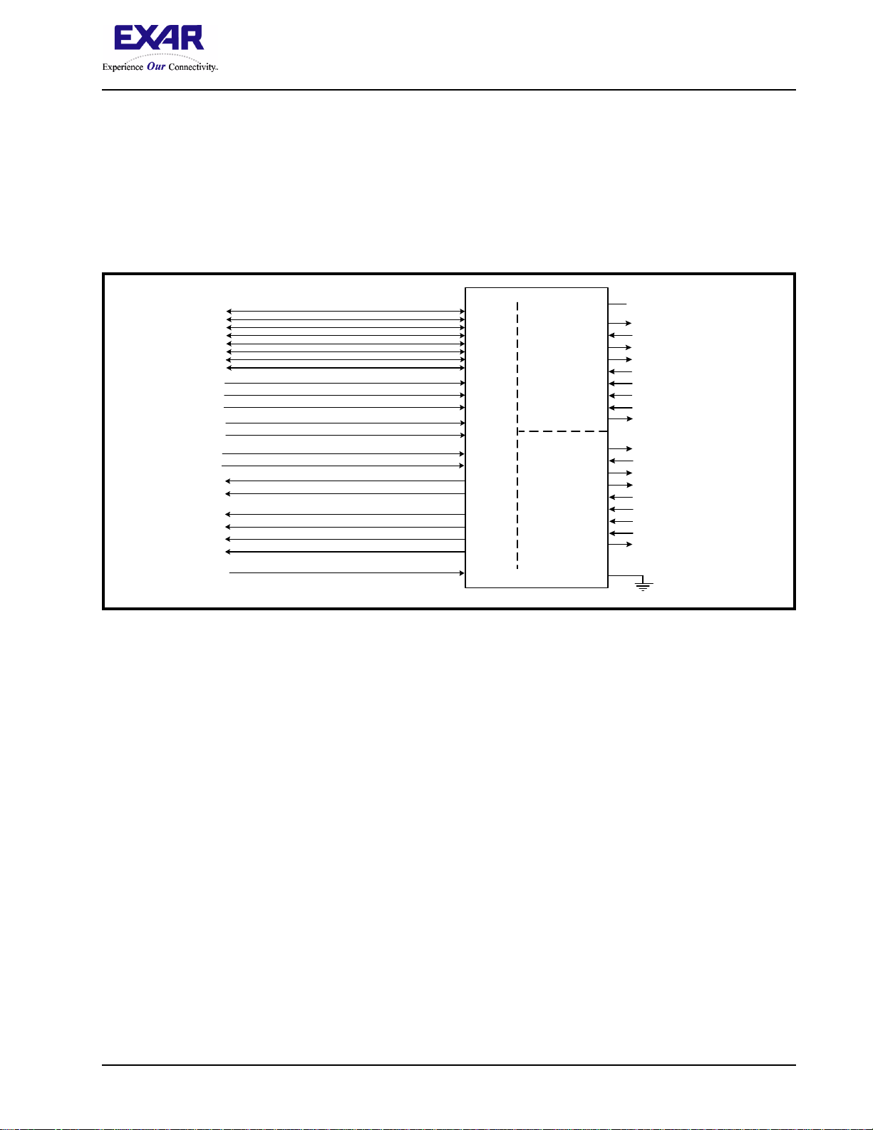
2.1 CPU Interface
The CPU interface is 8 data bits wide with 3 address lines and control signals to execute data bus read and
write transactions. The M2650 data interface supports the Intel compatible types of CPUs and it is compatible
to the industry standard 16C550 UART. No clock (oscillator nor external clock) is required to operate a data
bus transaction. Each bus cycle is asynchronous using CS#, IOR# and IOW# signals. Both UART channels
share the same data bus for host operations. The data bus interconnections are shown in
FIGURE 3. XR16M2650 DATA BUS INTERCONNECTIONS
Figure 3.
D0
D1
D2
D3
D4
D5
D6
D7
A0
A1
A2
IOR #
IOW #
UART_CSA#
UART_CSB#
UART_INTA
UART_INTB
TXRDYA#
RXRDYA#
TXRDYB#
RXRDYB#
UART_RESET
D0
D1
D2
D3
D4
D5
D6
D7
A0
A1
A2
IOR #
IOW #
CSA#
CSB#
INT A
INT B
TXRDYA#
RXRDYA#
TXRDYB#
RXRDYB#
RESET
UART
Channel A
UART
Channel B
VCC
TXA
RXA
DTRA#
RTSA#
CTSA#
DSRA#
CDA#
RIA#
OP2A#
TXB
RXB
DTRB#
RTSB#
CTSB#
DSRB#
CDB#
RIB#
OP2B#
GND
VCC
Seria l Interfac e of
RS-232, RS-422
Seria l Interfac e of
RS-232, RS-422
2.2 Device Reset
The RESET input resets the internal registers and the serial interface outputs in both channels to their default
state (see
Tab le 15). An active high pulse of longer than 40 ns duration will be required to activate the reset
function in the device.
2.3 Device Identification and Revision
The XR16M2650 provides a Device Identification code and a Device Revision code to distinguish the part from
other devices and revisions. To read the identification code from the part, it is required to set the baud rate
generator registers DLL and DLM both to 0x00 (DLD = 0xXX). Now reading the content of the DVID will
provide 0x06 for the XR16M2650 and reading the content of DREV will provide the revision of the part; for
example, a reading of 0x01 means revision A.
2.4 Channel A and B Selection
The UART provides the user with the capability to bi-directionally transfer information between an external
CPU and an external serial communication device. A LOW signal on the chip select pins, CSA# or CSB#,
allows the user to select UART channel A or B to configure, send transmit data and/or unload receive data to/
from the UART. Selecting both UARTs can be useful during power up initialization to write to the same internal
7
XR16M2650
HIGH PERFORMANCE LOW VOLTAGE DUART WITH 32-BYTE FIFO REV. 1.0.2
registers, but do not attempt to read from both uarts simultaneously. Individual channel select functions are
shown in
2.5 Channel A and B Internal Registers
Each UART channel in the M2650 has a set of enhanced registers for controlling, monitoring and data loading
and unloading. The configuration register set is compatible to those already available in the standard single
16C550 and dual ST16C2550. These registers function as data holding registers (THR/RHR), interrupt status
and control registers (ISR/IER), a FIFO control register (FCR), receive line status and control registers (LSR/
LCR), modem status and control registers (MSR/MCR), programmable data rate (clock) divisor registers (DLL/
DLM/DLD), and a user accessible Scratchpad Register (SPR).
Beyond the general 16C2550 features and capabilities, the M2650 offers enhanced feature registers (EFR,
Xon/Xoff 1, Xon/Xoff 2) that provide automatic RTS and CTS hardware flow control, and Xon/Xoff software flow
control. All the register functions are discussed in full detail later in
REGISTERS” on page 21.
Table 1.
TABLE 1: CHANNEL A AND B SELECT
CSA# CSB# FUNCTION
1 1 UART de-selected
0 1 Channel A selected
1 0 Channel B selected
0 0 Channel A and B selected
“Section 3.0, UART INTERNAL
2.6 DMA Mode
The device does not support direct memory access. The DMA Mode (a legacy term) in this document doesn’t
mean “direct memory access” but refers to data block transfer operation. The DMA mode affects the state of
the RXRDY# A/B and TXRDY# A/B output pins. The transmit and receive FIFO trigger levels provide additional
flexibility to the user for block mode operation. The LSR bits 5-6 provide an indication when the transmitter is
empty or has an empty location(s) for more data. The user can optionally operate the transmit and receive
FIFO in the DMA mode (FCR bit-3=1). When the transmit and receive FIFO are enabled and the DMA mode is
disabled (FCR bit-3 = 0), the M2650 is placed in single-character mode for data transmit or receive operation.
When DMA mode is enabled (FCR bit-3 = 1), the user takes advantage of block mode operation by loading or
unloading the FIFO in a block sequence determined by the selected trigger level. In this mode, the M2650 sets
the TXRDY# pin when the transmit FIFO becomes full, and sets the RXRDY# pin when the receive FIFO
becomes empty. The following table shows their behavior. Also see
Figures 17through 22.
TABLE 2: TXRDY# AND RXRDY# OUTPUTS IN FIFO AND DMA MODE
PINS
RXRDY# A/B LOW = 1 byte
TXRDY# A/B LOW = THR empty
FCR BIT-0=0
(FIFO DISABLED)
HIGH = no data
HIGH = byte in THR
FCR BIT-0=1 (FIFO ENABLED)
FCR BIT-3 = 0
(DMA MODE DISABLED)
LOW = at least 1 byte in FIFO
HIGH = FIFO empty
LOW = FIFO empty
HIGH = at least 1 byte in FIFO
FCR BIT-3 = 1
(DMA MODE ENABLED)
HIGH to LOW transition when FIFO reaches the
trigger level, or time-out occurs
LOW to HIGH transition when FIFO empties
LOW = FIFO has at least 1 empty location
HIGH = FIFO is full
8
XR16M2650
REV. 1.0.2 HIGH PERFORMANCE LOW VOLTAGE DUART WITH 32-BYTE FIFO
2.7 INTA and INTB Outputs
The INTA and INTB interrupt output changes according to the operating mode and enhanced features setup.
Table 3 and 4 summarize the operating behavior for the transmitter and receiver. Also see Figures 17
through 22.
TABLE 3: INTA AND INTB PINS OPERATION FOR TRANSMITTER
(FIFO DISABLED)
INTA/B Pin LOW = a byte in THR
HIGH = THR empty
INTA/B Pin LOW = a byte in THR
HIGH = transmitter empty
FCR BIT-0 = 0
LOW = FIFO above trigger level
HIGH = FIFO below trigger level or FIFO empty
LOW = FIFO above trigger level
HIGH = FIFO below trigger level or transmitter empty
FCR BIT-0 = 1 (FIFO ENABLED)
TABLE 4: INTA AND INTB PINS OPERATION FOR RECEIVER
INTA/B Pin LOW = no data
HIGH = 1 byte
FCR BIT-0 = 0
(FIFO DISABLED)
LOW = FIFO below trigger level
HIGH = FIFO above trigger level
FCR BIT-0 = 1
(FIFO ENABLED)
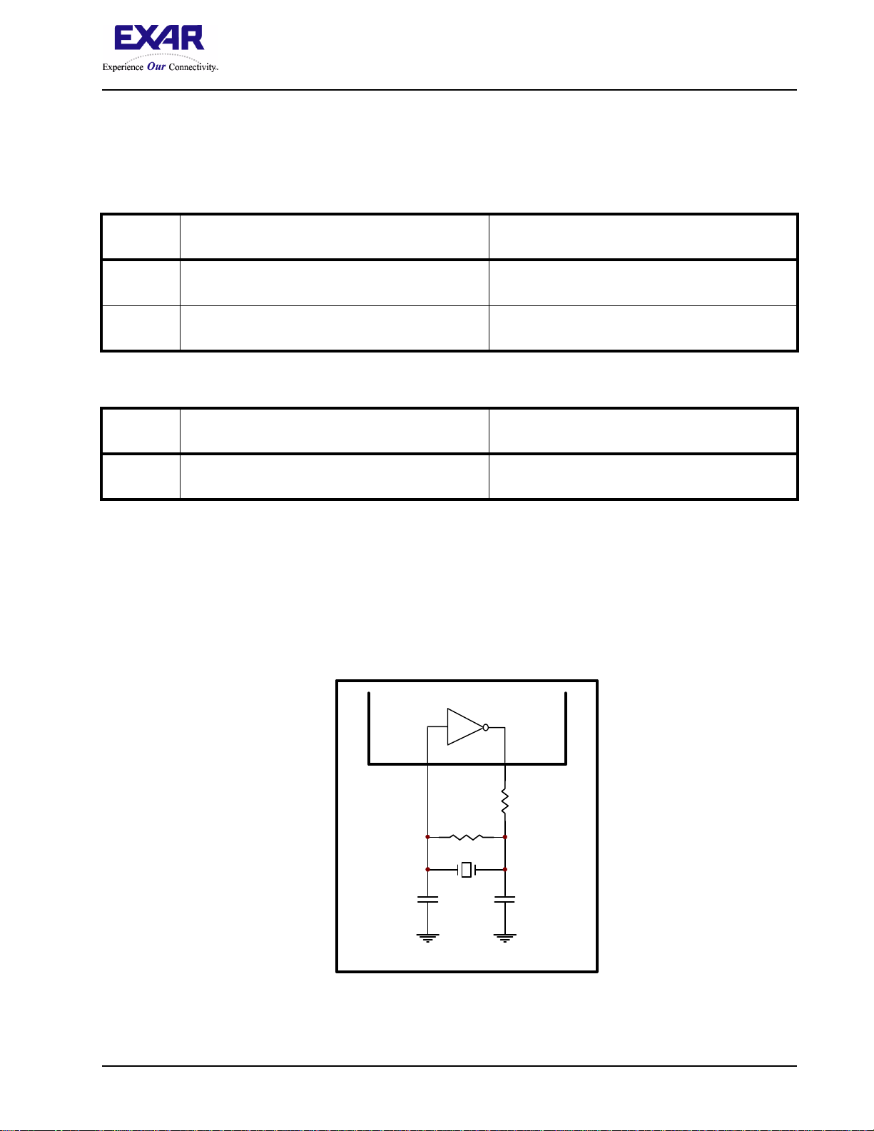
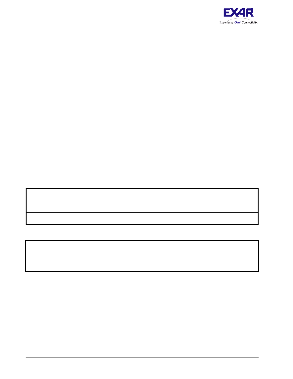
2.8 Crystal Oscillator or External Clock Input
The M2650 includes an on-chip oscillator (XTAL1 and XTAL2) to produce a clock for both UART sections in the
device. The CPU data bus does not require this clock for bus operation. The crystal oscillator provides a
system clock to the Baud Rate Generators (BRG) section found in each of the UART. XTAL1 is the input to the
oscillator or external clock buffer input with XTAL2 pin being the output. For programming details, see
“Section 2.9, Programmable Baud Rate Generator with Fractional Divisor” on page 10.
FIGURE 4. TYPICAL CRYSTAL CONNECTIONS
XTAL1 XTAL2
R2
500K - 1M
C1
22-47pF
22-47pF
9
Y1
C2
R1
0-120
(Optional)
1.8432 MHz
to
24 MHz
XR16M2650
HIGH PERFORMANCE LOW VOLTAGE DUART WITH 32-BYTE FIFO REV. 1.0.2
The on-chip oscillator is designed to use an industry standard microprocessor crystal (parallel resonant,
fundamental frequency with 10-22 pF capacitance load, ESR of 20-120 ohms and 100 ppm frequency
tolerance) connected externally between the XTAL1 and XTAL2 pins (see
Rate Generator is capable of operating with a crystal oscillator frequency of up to 24 MHz. However, with an
external clock input on XTAL1 pin, it can extend its operation up to 64 MHz (16 Mbps serial data rate) at 3.3V
with an 4X sampling rate. For further reading on the oscillator circuit please see the Application Note DAN108
on the EXAR web site at
http://www.exar.com.
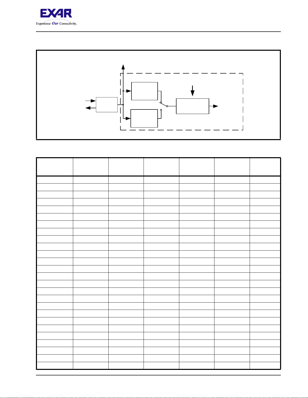
2.9 Programmable Baud Rate Generator with Fractional Divisor
Each UART has its own Baud Rate Generator (BRG) with a prescaler for the transmitter and receiver. The
prescaler is controlled by a software bit in the MCR register. The MCR register bit-7 sets the prescaler to divide
the input crystal or external clock by 1 or 4. The output of the prescaler clocks to the BRG. The BRG further
divides this clock by a programmable divisor between 1 and (216 - 0.0625) in increments of 0.0625 (1/16) to
obtain a 16X or 8X or 4X sampling clock of the serial data rate. The sampling clock is used by the transmitter
for data bit shifting and receiver for data sampling. The BRG divisor (DLL, DLM and DLD registers) defaults to
the value of ’1’ (DLL = 0x01, DLM = 0x00 and DLD = 0x00) upon reset. Therefore, the BRG must be
programmed during initialization to the operating data rate. The DLL and DLM registers provide the integer part
of the divisor and the DLD register provides the fractional part of the divisor. Only the four lower bits of the DLD
are implemented and they are used to select a value from 0 (for setting 0000) to 0.9375 or 15/16 (for setting
1111). Programming the Baud Rate Generator Registers DLL, DLM and DLD provides the capability for
selecting the operating data rate.
Table 5 shows the standard data rates available with a 24MHz crystal or
external clock at 16X clock rate. If the pre-scaler is used (MCR bit-7 = 1), the output data rate will be 4 times
less than that shown in
Table 5. At 8X sampling rate, these data rates would double. And at 4X sampling rate,
they would quadruple. Also, when using 8X sampling mode, please note that the bit-time will have a jitter (+/- 1/
16) whenever the DLD is non-zero and is an odd number. When using a non-standard data rate crystal or
external clock, the divisor value can be calculated with the following equation(s):
Figure 4). The programmable Baud
Required Divisor (decimal)=(XTAL1 clock frequency / prescaler) /(serial data rate x 16), with 16X mode, DLD[5:4]=’00’
Required Divisor (decimal)= (XTAL1 clock frequency / prescaler / (serial data rate x 8), with 8X mode, DLD[5:4] = ’01’
Required Divisor (decimal)= (XTAL1 clock frequency / prescaler / (serial data rate x 4), with 4X mode, DLD[5:4] = ’10’
The closest divisor that is obtainable in the M2650 can be calculated using the following formula:
ROUND( (Required Divisor - TRUNC(Required Divisor) )*16)/16 + TRUNC(Required Divisor), where
DLM = TRUNC(Required Divisor) >> 8
DLL = TRUNC(Required Divisor) & 0xFF
DLD = ROUND( (Required Divisor-TRUNC(Required Divisor) )*16)
In the formulas above, please note that:
TRUNC (N) = Integer Part of N. For example, TRUNC (5.6) = 5.
ROUND (N) = N rounded towards the closest integer. For example, ROUND (7.3) = 7 and ROUND (9.9) = 10.
A >> B indicates right shifting the value ’A’ by ’B’ number of bits. For example, 0x78A3 >> 8 = 0x0078.
10
XR16M2650
REV. 1.0.2 HIGH PERFORMANCE LOW VOLTAGE DUART WITH 32-BYTE FIFO
FIGURE 5. BAUD RATE GENERATOR
To Other
Channel
DLL, DLM and DLD
Registers
Prescaler
Divide by 1
XTAL1
XTAL2
Crystal
Osc/
Buffer
Prescaler
Divide by 4
TABLE 5: TYPICAL DATA RATES WITH A 24 MHZ CRYSTAL OR EXTERNAL CLOCK AT 16X SAMPLING
MCR Bit-7=0
(default)
Fractional Baud
Rate Generator
MCR Bit-7=1
Logic
16X or 8X or 4X
Sampling
Rate Clock
to Transmitter
and Receiver
Required
Output Data
Rate
DIVISOR FOR 16x
Clock
(Decimal)
DIVISOR
OBTAINABLE IN
M2650
DLM PROGRAM
VALUE (HEX)
DLL PROGRAM
VALUE (HEX)
DLD PROGRAM
VALUE (HEX)
DATA ERROR
400 3750 3750 E A6 0 0
2400 625 625 2 71 0 0
4800 312.5 312 8/16 1 38 8 0
9600 156.25 156 4/16 0 9C 4 0
10000 150 150 0 96 0 0
19200 78.125 78 2/16 0 4E 2 0
25000 60 60 0 3C 0 0
28800 52.0833 52 1/16 0 34 1 0.04
38400 39.0625 39 1/16 0 27 1 0
50000 30 30 0 1E 0 0
57600 26.0417 26 1/16 0 1A 1 0.08
75000 20 20 0 14 0 0
100000 15 15 0 F 0 0
115200 13.0208 13 0 D 0 0.16
153600 9.7656 9 12/16 0 9 C 0.16
200000 7.5 7 8/16 0 7 8 0
225000 6.6667 6 11/16 0 6 B 0.31
230400 6.5104 6 8/16 0 6 8 0.16
250000 6 6 0 6 0 0
300000 5 5 0 5 0 0
400000 3.75 3 12/16 0 3 C 0
460800 3.2552 3 4/16 0 3 4 0.16
500000 3 3 0 3 0 0
750000 2 2 0 2 0 0
921600 1.6276 1 10/16 0 1 A 0.16
1000000 1.5 1 8/16 0 1 8 0
RATE (%)
11
XR16M2650
HIGH PERFORMANCE LOW VOLTAGE DUART WITH 32-BYTE FIFO REV. 1.0.2
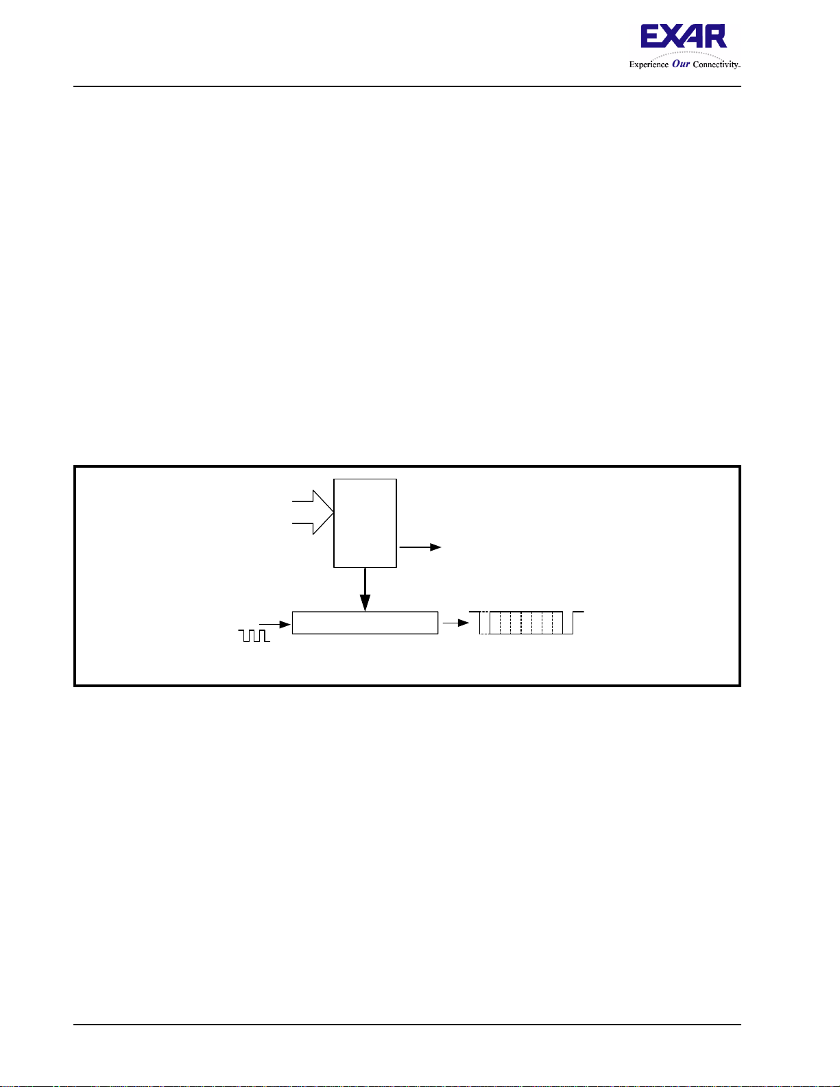
2.10 Transmitter
The transmitter section comprises of an 8-bit Transmit Shift Register (TSR) and 32 bytes of FIFO which
includes a byte-wide Transmit Holding Register (THR). TSR shifts out every data bit with the 16X/8X/4X
internal clock. A bit time is 16/8/4 clock periods (see DLD). The transmitter sends the start-bit followed by the
number of data bits, inserts the proper parity-bit if enabled, and adds the stop-bit(s). The status of the FIFO and
TSR are reported in the Line Status Register (LSR bit-5 and bit-6).
2.10.1 Transmit Holding Register (THR) - Write Only
The transmit holding register is an 8-bit register providing a data interface to the host processor. The host
writes transmit data byte to the THR to be converted into a serial data stream including start-bit, data bits,
parity-bit and stop-bit(s). The least-significant-bit (Bit-0) becomes first data bit to go out. The THR is the input
register to the transmit FIFO of 32 bytes when FIFO operation is enabled by FCR bit-0. Every time a write
operation is made to the THR, the FIFO data pointer is automatically bumped to the next sequential data
location.
2.10.2 Transmitter Operation in non-FIFO Mode
The host loads transmit data to THR one character at a time. The THR empty flag (LSR bit-5) is set when the
data byte is transferred to TSR. THR flag can generate a transmit empty interrupt (ISR bit-1) when it is enabled
by IER bit-1. The TSR flag (LSR bit-6) is set when TSR becomes completely empty.
FIGURE 6. TRANSMITTER OPERATION IN NON-FIFO MODE
Data
Byte
16X or 8X or 4X
Clock
( DLD[5:4] )
Transmit Shift Register (TSR)
Transmit
Holding
Register
(THR)
THR Interrupt (ISR bit-1)
Enabled by IER bit-1
M
S
B
L
S
B
TXNOFIFO1
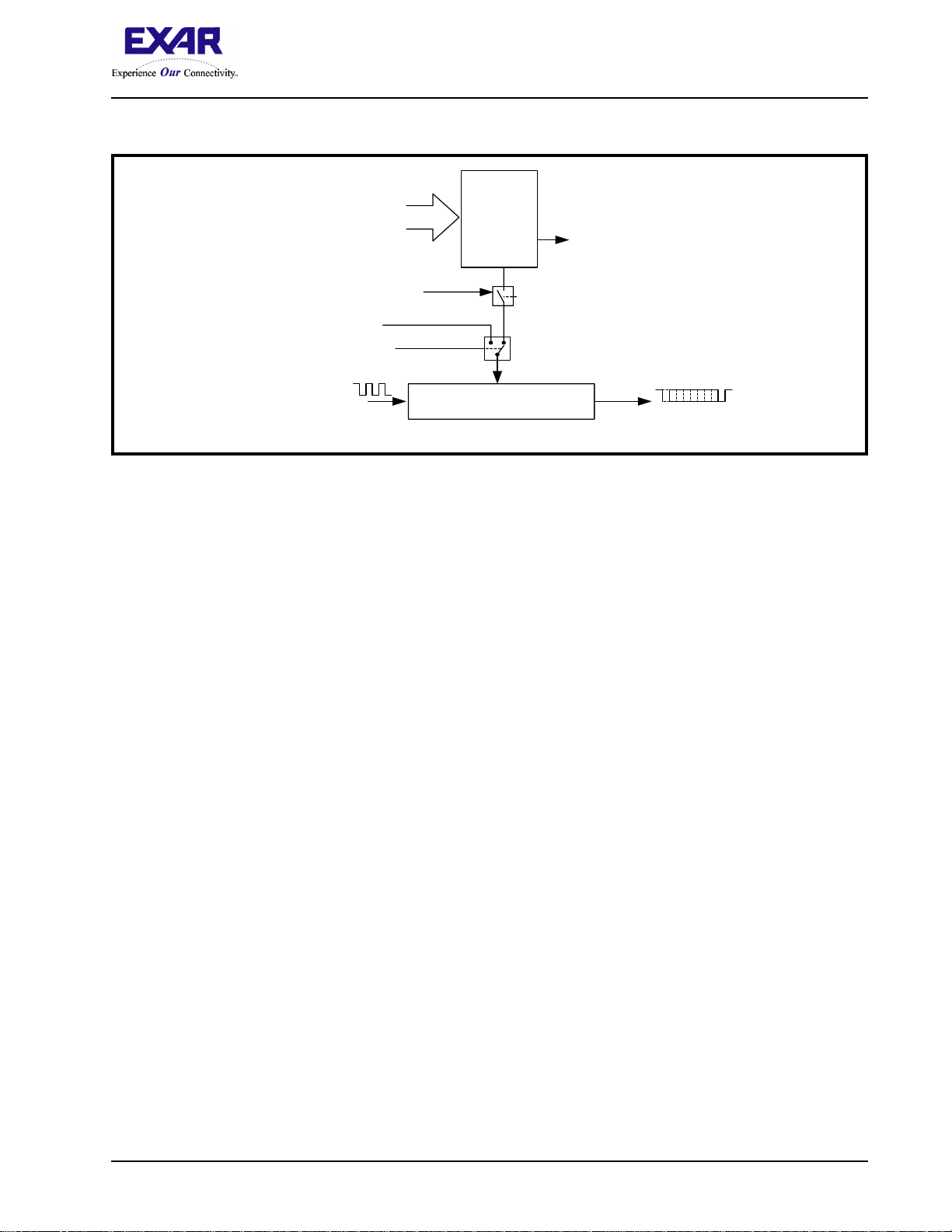
2.10.3 Transmitter Operation in FIFO Mode
The host may fill the transmit FIFO with up to 32 bytes of transmit data. The THR empty flag (LSR bit-5) is set
whenever the FIFO is empty. The THR empty flag can generate a transmit empty interrupt (ISR bit-1) when the
amount of data in the FIFO falls below its selected trigger level. The transmit empty interrupt is enabled by IER
bit-1. The TSR flag (LSR bit-6) is set when TSR/FIFO becomes empty.
12
XR16M2650
REV. 1.0.2 HIGH PERFORMANCE LOW VOLTAGE DUART WITH 32-BYTE FIFO
FIGURE 7. TRANSMITTER OPERATION IN FIFO AND FLOW CONTROL MODE
Transmit
Data Byte
Auto CTS Flow Control (CTS# pin)
Flow Control Characters
(Xoff1/2 and Xon1/2 Reg.)
Auto Softw are Flow Con trol
16X or 8X or 4X Clock
(DLD[5:4])
Transmit Data Shift Register
Transmit
FIFO
(TSR )
THR Interrupt (ISR bit-1) falls
below the programmed Trigger
Level and then when becomes
empty. FIFO is Enabled by FCR
bit-0=1
TXFIFO1
2.11 Receiver
The receiver section contains an 8-bit Receive Shift Register (RSR) and 32 bytes of FIFO which includes a
byte-wide Receive Holding Register (RHR). The RSR uses the 16X/8X/4X clock (DLD[5:4]) for timing. It
verifies and validates every bit on the incoming character in the middle of each data bit. On the falling edge of
a start or false start bit, an internal receiver counter starts counting at the 16X/8X/4X clock rate. After 8 clocks
(or 4 if 8X or 2 if 4X) the start bit period should be at the center of the start bit. At this time the start bit is
sampled and if it is still LOW it is validated. Evaluating the start bit in this manner prevents the receiver from
assembling a false character. The rest of the data bits and stop bits are sampled and validated in this same
manner to prevent false framing. If there were any error(s), they are reported in the LSR register bits 2-4. Upon
unloading the receive data byte from RHR, the receive FIFO pointer is bumped and the error tags are
immediately updated to reflect the status of the data byte in RHR register. RHR can generate a receive data
ready interrupt upon receiving a character or delay until it reaches the FIFO trigger level. Furthermore, data
delivery to the host is guaranteed by a receive data ready time-out interrupt when data is not received for 4
word lengths as defined by LCR[1:0] plus 12 bits time. This is equivalent to 3.7-4.6 character times. The RHR
interrupt is enabled by IER bit-0. See
Figure 8 and Figure 9 below.
2.11.1 Receive Holding Register (RHR) - Read-Only
The Receive Holding Register is an 8-bit register that holds a receive data byte from the Receive Shift
Register. It provides the receive data interface to the host processor. The RHR register is part of the receive
FIFO of 32 bytes by 11-bits wide, the 3 extra bits are for the 3 error tags to be reported in LSR register. When
the FIFO is enabled by FCR bit-0, the RHR contains the first data character received by the FIFO. After the
RHR is read, the next character byte is loaded into the RHR and the errors associated with the current data
byte are immediately updated in the LSR bits 2-4.
13
XR16M2650
HIGH PERFORMANCE LOW VOLTAGE DUART WITH 32-BYTE FIFO REV. 1.0.2
FIGURE 8. RECEIVER OPERATION IN NON-FIFO MODE
16X or 8X or 4X Clock
( DLD[5:4] )
Receive D ata Sh ift
Register (RSR)
Data B it
Valida tio n
Receive D a ta C h arac ters
Receive
Data Byte
and Errors
Erro r
Tags in
LSR bits
4:2
Receive Data
Holding R egiste r
(RHR)
RHR Interrupt (IS R bit-2 )
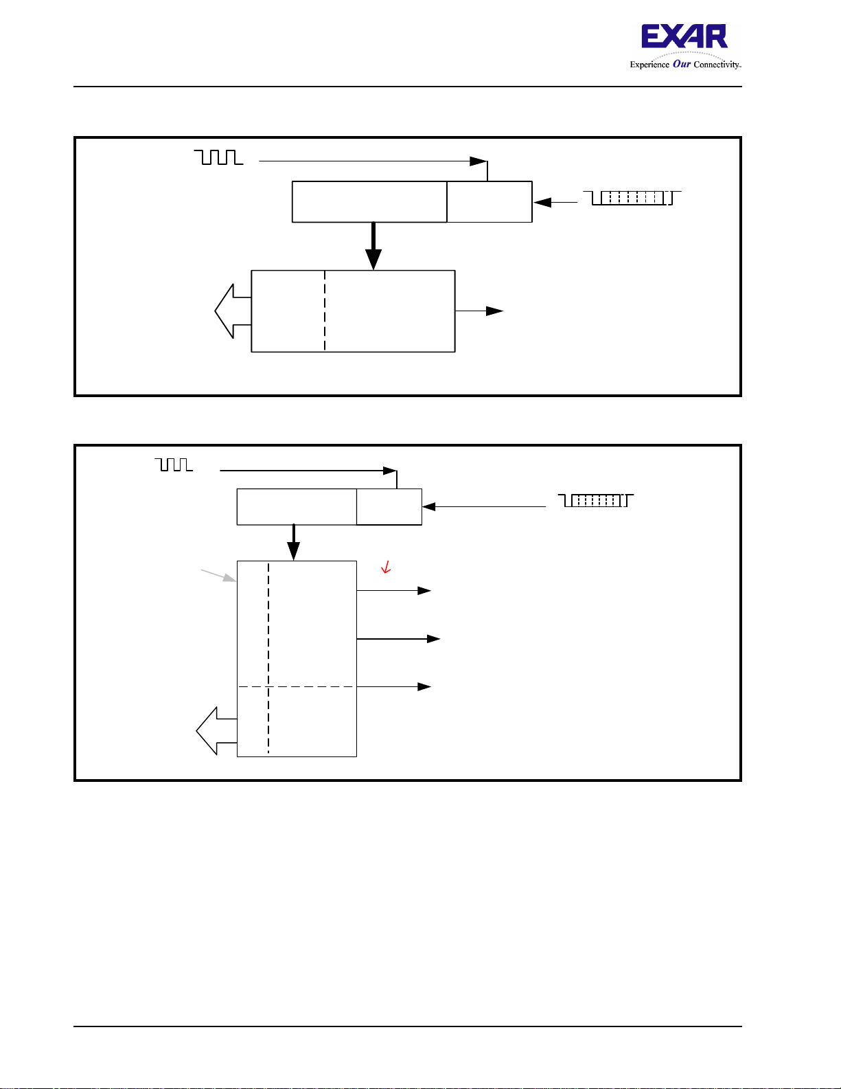
FIGURE 9. RECEIVER OPERATION IN FIFO AND AUTO RTS FLOW CONTROL MODE
16X or 8X or 4X Clock
( DLD[5:4] )
32 bytes by 11-bit
wide FIFO
Receive Data
Byte and Errors
Receive Data Shift
Register (RSR)
Receive
Data FIFO
(32-sets)
Error Tags
Receive
Data
LSR bits 4:2
Error Tags in
Data Bit
Validation
Example
- RX FIFO trigger level selected at 16 bytes
:
Data falls to
8
FIFO
Trigger=16
Data fills to
24
(See Note Below)
RTS# re-asserts when data falls below the flow
control trigger level to restart remote transmitter.
Enable by EFR bit-6=1, MCR bit-1.
RHR Interrupt (ISR bit-2) programmed for
desired FIFO trigger level.
FIFO is Enabled by FCR bit-0=1
RTS# de-asserts when data fills above the flow
control trigger level to suspend remote transmitter.
Enable by EFR bit-6=1, MCR bit-1.
RXFIFO1
Receive Data Characters
RXFIFO1
14
XR16M2650
REV. 1.0.2 HIGH PERFORMANCE LOW VOLTAGE DUART WITH 32-BYTE FIFO
2.12 Auto RTS (Hardware) Flow Control
Automatic RTS hardware flow control is used to prevent data overrun to the local receiver FIFO. The RTS#
output is used to request remote unit to suspend/resume data transmission. The auto RTS flow control
features is enabled to fit specific application requirement (see
• Enable auto RTS flow control using EFR bit-6.
• The auto RTS function must be started by asserting RTS# output pin (MCR bit-1 to HIGH after it is enabled).
If using the Auto RTS interrupt:
• Enable RTS interrupt through IER bit-6 (after setting EFR bit-4). The UART issues an interrupt when the
RTS# pin makes a transition from low to high: ISR bit-5 will be set to HIGH.
2.13 Auto RTS Hysteresis
The M2650 has a new feature that provides flow control trigger hysteresis while maintaining compatibility with
the XR16C850, ST16C650A and ST16C550 family of UARTs. With the Auto RTS function enabled, an interrupt
is generated when the receive FIFO reaches the selected RX trigger level. The RTS# pin will not be forced
HIGH (RTS off) until the receive FIFO reaches one trigger level above the selected trigger level in the trigger
table (
Tab le 11). The RTS# pin will return LOW after the RX FIFO is unloaded to one level below the selected
trigger level. Under the above described conditions, the M2650 will continue to accept data until the receive
FIFO gets full. The Auto RTS function is initiated when the RTS# output pin is asserted LOW (RTS On).
Figure 10):
TABLE 6: AUTO RTS (HARDWARE) FLOW CONTROL
RX TRIGGER LEVEL INT PIN ACTIVATION
8 8 16 0
16 16 24 8
24 24 28 16
28 28 28 24
2.14 Auto CTS Flow Control
Automatic CTS flow control is used to prevent data overrun to the remote receiver FIFO. The CTS# input is
monitored to suspend/restart the local transmitter. The auto CTS flow control feature is selected to fit specific
application requirement (see
Figure 10):
RTS# DE-ASSERTED (HIGH)
(CHARACTERS IN RX FIFO)
RTS# ASSERTED (LOW)
(CHARACTERS IN RX FIFO)
• Enable auto CTS flow control using EFR bit-7.
If using the Auto CTS interrupt:
• Enable CTS interrupt through IER bit-7 (after setting EFR bit-4). The UART issues an interrupt when the
CTS# pin is de-asserted (HIGH): ISR bit-5 will be set to 1, and UART will suspend transmission as soon as
the stop bit of the character in process is shifted out. Transmission is resumed after the CTS# input is reasserted (LOW), indicating more data may be sent.
15
 Loading...