

EXAR XR16L2752 Service Manual
查询XR16L2752供应商
xr
AUGUST 2004 REV. 1.2.0
GENERAL DESCRIPTION
The XR16L27521 (2752) is a low voltage dual
universal asynchronous receiver and transmitter
(UART) with 5 Volt tolerant inputs. The device
operates from 2.25 to 5.5 Volt supply range and is
pin-to-pin compatible to Exar’s ST16C2552 and
XR16C2852. The 2752 register set is compatible to
the ST16C2552 and the XR16C2852 enhanced
features. It supports the Exar’s enhanced features of
64 bytes of TX and RX FIFOs, programmable FIFO
trigger level and FIFO level counters, automatic
hardware (RTS/CTS) and software flow control,
automatic RS-485 half duplex direction control output
and a complete modem interface. Onboard registers
provide the user with operational status and data
error flags. An internal loopback capability allows
system diagnostics. Independent programmable
baud rate generators are provided in each channel to
select data rates up to 6.25 Mbps at 5 Volt and 8X
sampling. The 2752 is available in the 44-pin PLCC
package.
OTE
1 Covered by U.S. Patent #5,649,122 and #5,949,787
N
:
APPLICATIONS
Portable Appliances
•
Telecommunication Network Routers
•
Ethernet Network Routers
•
Cellular Data Devices
•
Factory Automation and Process Controls
•
XR16L2752
2.25V TO 5.5V DUART WITH 64-BYTE FIFO
FEATURES
•
2.25 to 5.5 Volt Operation
•
5 Volt Tolerant Inputs
Pin-to-pin compatible to Exar’s ST16C2552 and
•
XR16C2852
• Larger FIFO version of PC16C552
Two independent UART channels
•
Reg set compatible to 16C2552 and 16C2852
■
Up to 6.25 Mbps at 5 Volt, 4 Mbps at 3.3 Volt
■
and 3 Mbps at 2.5 Volt with 8X sampling rate
Transmit and Receive FIFOs of 64 bytes
■
Programmable TX and RX FIFO Trigger Levels
■
Transmit and Receive FIFO Level Counters
■
Automatic Hardware (RTS/CTS) Flow Control
■
Selectable Auto RTS Flow Control Hysteresis
■
Automatic Software (Xon/Xoff) Flow Control
■
Automatic RS-485 Half-duplex Direction
■
Control Output via RTS#
Wireless Infrared (IrDA 1.0) Encoder/Decoder
■
Automatic sleep mode
■
Full modem interface
■
Alternate Function Register
•
Device Identification and Revision
•
Crystal oscillator or external clock input
•
Industrial and commercial temperature ranges
•
44-PLCC package
•
F
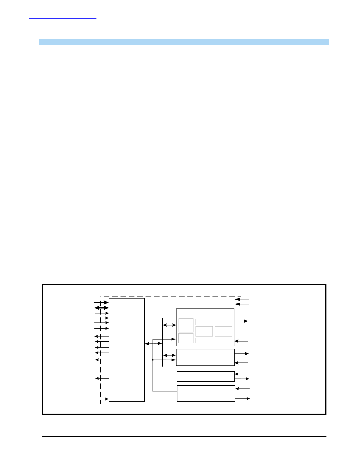
IGURE 1. XR16L2752 BLOCK DIAGRAM
A2:A0
D7:D0
IOR#
IOW#
CS#
CHSEL
INTA
INTB
TXRDYA#
TXRDYB#
MFA#
(OP2A#,
BAUDOUTA#, or
RXRDYA#)
MFB#
(OP2B#,
BAUDOUTB#, or
RXRDYB#)
Reset
Corporation 48720 Kato Road, Fremont CA, 94538 • (510) 668-7000 • FAX (510) 668-7017 • www.exar.com
Exar
8-bit Data
Bus
Interface
*5 Volt Tolerant Inputs
(Except External Clock Input)
UART Channel A
64 Byte TX FIFO
UART
Regs
TX & RX
BRG
64 Byte RX FIFO
UART Channel B
(same as Channel A)
Crystal Osc/Buffer
Modem Control Logic
IR
ENDEC
2.25 V to 5.5 V VCC
GND
TXA (or TXIRA)
RXA (or RXIRA)
TXB (or TXIRB)
RXB (or RXIRB)
XTAL1
XTAL2
CTS#A/B, RI#A/B,
CD#A/B, DSR#A/B
DTR#A/B, RTS#A/B
2752BLK
XR16L2752
2.25V TO 5.5V DUART WITH 64-BYTE FIFO
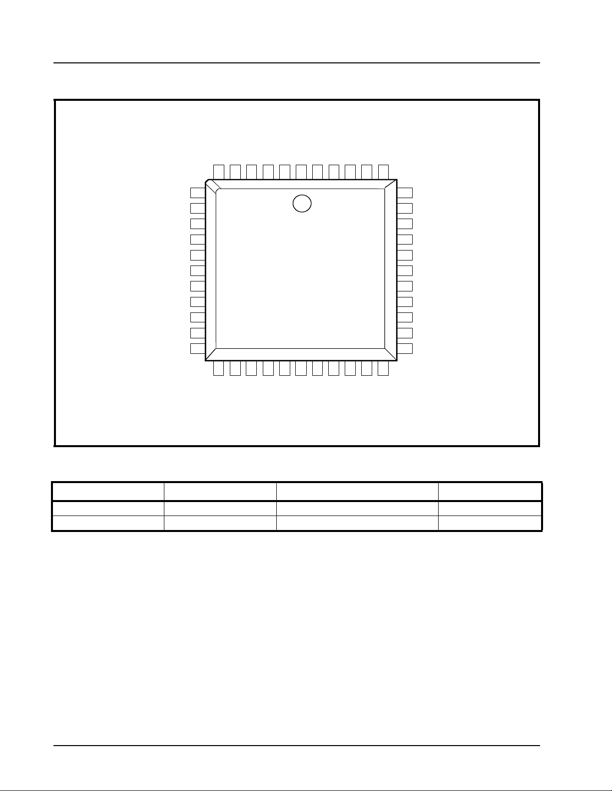
FIGURE 2. PIN OUT ASSIGNMENT
D4
D3
6
5
7
D5
8
D6
9
D7
10
A0
11
XTAL1
12
GND
13
XTAL2
14
A1
15
A2
INTB
16
17
CHSEL
D2
D1
4
3
XR16L2752
44-pin PLCC
D0
2
xr
REV. 1.2.0
TXRDYA#
VCC
RIA#
CDA#
DSRA#
CTSA#
1
44
43
42
41
40
39
RXA
38
TXA
37
DTRA#
36
RTSA#
35
MFA#
34
INTA
VCC
33
32
TXRDYB#
31
RIB#
30
CDB#
29
DSRB#
18
19
20
21
22
23
24
25
26
27
28
CS#
IOW#
MFB#
RESET
GND
RTSB#
IOR#
TXB
RXB
CTSB#
DTRB#
ORDERING INFORMATION
P
ART NUMBER
XR16L2752CJ 44-Lead PLCC 0°C to +70°C Active
XR16L2752IJ 44-Lead PLCC -40°C to +85°C Active
P
ACKAGE
O
PERATING TEMPERATURE RANGE
D
EVICE STATUS
2

xr
REV. 1.2.0
PIN DESCRIPTIONS
Pin Description
XR16L2752
2.25V TO 5.5V DUART WITH 64-BYTE FIFO
N
AME
DATA BUS INTERFACE
A2
A1
A0
D7
D6
D5
D4
D3
D2
D1
D0
IOR# 24 I Input/Output Read Strobe (active low). The falling edge instigates an internal read
IOW# 20 I Input/Output Write Strobe (active low). The falling edge instigates an internal write
CS# 18 I UART chip select (active low). This function selects channel A or B in accordance
CHSEL 16 I Channel Select - UART channel A or B is selected by the logical state of this pin when
INTA 34 O UART channel A Interrupt output (active high). A logic high indicates channel A is
INTB 17 O UART channel B Interrupt output (active high). A logic high indicates channel B is
TXRDYA# 1 O
44-PLCC
P
#
IN
15
14
10
9
8
7
6
5
4
3
2
T
YPE
I Address data lines [2:0]. These 3 address lines select one of the internal registers in
UART channel A/B during a data bus transaction.
I/O Data bus lines [7:0] (bidirectional).
cycle and retrieves the data byte from an internal register pointed to by the address
lines [A2:A0]. The data byte is placed on the data bus to allow the host processor to
read it on the rising edge.
cycle and the rising edge transfers the data byte on the data bus to an internal register pointed by the address lines.
with the logical state of the CHSEL pin. This allows data to be transferred between
the user CPU and the 2752.
the CS# pin is a logic 0. A logic 0 on the CHSEL selects the UART channel B while a
logic 1 selects UART channel A. Normally, CHSEL could just be an address line from
the user CPU such as A4. Bit-0 of the Alternate Function Register (AFR) can temporarily override CHSEL function, allowing the user to write to both channel register
simultaneously with one write cycle when CS# is low. It is especially useful during the
initialization routine.
requesting for service. For more details, see
requesting for service. For more details, see
D
ESCRIPTION
Figures 18- 23
Figures 18- 23
.
.
UART channel A Transmitter Ready (active low). The output provides the TX
FIFO/THR status for transmit channel A. See Table 2 on page 8.
TXRDYB# 32 O UART channel B Transmitter Ready (active low). The output provides the TX FIFO/
THR status for transmit channel B.
MODEM OR SERIAL I/O INTERFACE
TXA 38 O
UART channel A Transmit Data or infrared encoder data. Standard transmit and
receive interface is enabled when MCR[6] = 0. In this mode, the TX signal will be
HIGH during reset or idle (no data). Infrared IrDA transmit and receive interface is
enabled when MCR[6] = 1. In the Infrared mode, the inactive state (no data) for the
Infrared encoder/decoder interface is LOW. If it is not used, leave it unconnected.
See Table 2 on page 8.
3

XR16L2752
2.25V TO 5.5V DUART WITH 64-BYTE FIFO
Pin Description
xr
REV. 1.2.0
N
AME
RXA 39 I
RTSA# 36 O UART channel A Request-to-Send (active low) or general purpose output. This output
CTSA# 40 I UART channel A Clear-to-Send (active low) or general purpose input. It can be used
DTRA# 37 O UART channel A Data-Terminal-Ready (active low) or general purpose output. If this
DSRA# 41 I UART channel A Data-Set-Ready (active low) or general purpose input. This input
CDA# 42 I
RIA# 43 I
MFA# 35 O Multi-Function Output Channel A. This output pin can function as the OP2A#, BAUD-
44-PLCC
PIN #
T
YPE
UART channel A Receive Data or infrared receive data. Normal receive data input
must idle HIGH. The infrared receiver pulses typically idles LOW but can be inverted
by software control prior going in to the decoder, see MCR[6] and FCTR[2]. If this pin
is not used, tie it to VCC or pull it high via a 100k ohm resistor.
must be asserted prior to using auto RTS flow control, see EFR[6], MCR[1],
FCTR[1:0], EMSR[5:4] and IER[6]. For auto RS485 half-duplex direction control, see
FCTR[3] and EMSR[3].
for auto CTS flow control, see EFR[7], and IER[7]. This input should be connected to
VCC when not used.
pin is not used, leave it unconnected.
should be connected to VCC when not used. This input has no effect on the UART.
UART channel A Carrier-Detect (active low) or general purpose input. This input
should be connected to VCC when not used. This input has no effect on the UART.
UART channel A Ring-Indicator (active low) or general purpose input. This input
should be connected to VCC when not used. This input has no effect on the UART.
OUTA#, or RXRDYA# pin. One of these output signal functions can be selected by
the user programmable bits 1-2 of the Alternate Function Register (AFR). These signal functions are described as follows:
D
ESCRIPTION
1) OP2A# - When OP2A# (active low) is selected, the MF# pin is LOW when MCR bit3 is set to a logic 1 (see MCR bit-3). MCR bit-3 defaults to a logic 1 condition after a
reset or power-up.
2) BAUDOUTA# - When BAUDOUTA# function is selected, the 16X Baud rate clock
output is available at this pin.
3) RXRDYA# - RXRDYA# (active low) is intended for monitoring DMA data transfers.
Table 2 on page 8
See
TXB 26 O
RXB 25 I
RTSB# 23 O UART channel B Request-to-Send (active low) or general purpose output. This port
UART channel B Transmit Data or infrared encoder data. Standard transmit and
receive interface is enabled when MCR[6] = 0. In this mode, the TX signal will be
HIGH during reset or idle (no data). Infrared IrDA transmit and receive interface is
enabled when MCR[6] = 1. In the Infrared mode, the inactive state (no data) for the
Infrared encoder/decoder interface is LOW. If it is not used, leave it unconnected.
UART channel B Receive Data or infrared receive data. Normal receive data input
must idle HIGH. The infrared receiver pulses typically idles LOW but can be inverted
by software control prior going in to the decoder, see MCR[6] and FCTR[2]. If this pin
is not used, tie it to VCC or pull it high via a 100k ohm resistor.
must be asserted prior to using auto RTS flow control, see EFR[6], MCR[1],
FCTR[1:0], EMSR[5:4] and IER[6]. For auto RS485 half-duplex direction control, see
FCTR[3] and EMSR[3].
for more details.
4
xr
REV. 1.2.0
Pin Description
XR16L2752
2.25V TO 5.5V DUART WITH 64-BYTE FIFO
N
AME
CTSB# 28 I UART channel B Clear-to-Send (active low) or general purpose input. It can be used
DTRB# 27 O UART channel B Data-Terminal-Ready (active low) or general purpose output. If this
DSRB# 29 I UART channel B Data-Set-Ready (active low) or general purpose input. This input
CDB# 30 I
RIB# 31 I
MFB# 19 O Multi-Function Output Channel B. This output pin can function as the OP2B#, BAUD-
44-PLCC
PIN #
T
YPE
for auto CTS flow control, see EFR[7], and IER[7]. This input should be connected to
VCC when not used.
pin is not used, leave it unconnected.
should be connected to VCC when not used. This input has no effect on the UART.
UART channel B Carrier-Detect (active low) or general purpose input. This input
should be connected to VCC when not used. This input has no effect on the UART.
UART channel B Ring-Indicator (active low) or general purpose input. This input
should be connected to VCC when not used. This input has no effect on the UART.
OUTB#, or RXRDYB# pin. One of these output signal functions can be selected by
the user programmable bits 1-2 of the Alternate Function Register (AFR). These signal functions are described as follows:
1) OP2B# - When OP2B# (active low) is selected, the MF# pin is LOW when MCR bit3 is set HIGH (see MCR bit-3). MCR bit-3 defaults to a logic 1 condition after a reset
or power-up.
2) BAUDOUTB# - When BAUDOUTB# function is selected, the 16X Baud rate clock
output is available at this pin.
D
ESCRIPTION
3) RXRDYB# - RXRDYB# (active low) is intended for monitoring DMA data transfers.
Table 2 on page 8
See
ANCILLARY SIGNALS
XTAL1 11 I Crystal or external clock input. Caution: this input is not 5V tolerant.
XTAL2 13 O Crystal or buffered clock output.
RESET 21 I Reset (active high) - A longer than 40 ns HIGH pulse on this pin will reset the internal
registers and all outputs. The UART transmitter output will be held HIGH, the receiver
input will be ignored and outputs are reset during reset period (see External Reset
Conditions).
VCC 44, 33 Pwr 2.25 to 5.5V power supply. All input pins, except XTAL1, are 5V tolerant.
GND 22, 12 Pwr Power supply common, ground.
for more details.
Pin type: I=Input, O=Output, I/O= Input/output, OD=Output Open Drain.
5

XR16L2752
2.25V TO 5.5V DUART WITH 64-BYTE FIFO
1.0 PRODUCT DESCRIPTION
The XR16L2752 (2752) integrates the functions of 2 enhanced 16C550 Universal Asynchronous Receiver and
Transmitter (UART). Each UART is independently controlled having its own set of device configuration
registers. The configuration registers set is 16550 UART compatible for control, status and data transfer.
Additionally, each UART channel has 64-bytes of transmit and receive FIFOs, automatic RTS/CTS hardware
flow control with hysteresis control, automatic Xon/Xoff and special character software flow control,
programmable transmit and receive FIFO trigger levels, FIFO level counters, infrared encoder and decoder
(IrDA ver 1.0), programmable baud rate generator with a prescaler of divide by 1 or 4, and data rate up to 6.25
Mbps with 8X sampling clock rate or 3.125 Mbps in the 16X rate. The XR16L2752 is a 2.25 to 5.5V device with
5 volt tolerant inputs. The 2752 is fabricated with an advanced CMOS process.
Enhanced Features
The 2752 DUART provides a solution that supports 64 bytes of transmit and receive FIFO memory, instead of
128 bytes provided in the XR16C2852 and 16 bytes in the ST16C2552. The 2752 is designed to work with low
supply voltage and high performance data communication systems, that require fast data processing time.
Increased performance is realized in the 2752 by the larger transmit and receive FIFOs, FIFO trigger level
control, FIFO level counters and automatic flow control mechanism. This allows the external processor to
handle more networking tasks within a given time. For example, the ST16C2552 with a 16 byte FIFO, unloads
16 bytes of receive data in 1.53 ms (This example uses a character length of 11 bits, including start/stop bits at
115.2 Kbps). This means the external CPU will have to service the receive FIFO at 1.53 ms intervals. However
with the 64 byte FIFO in the 2752, the data buffer will not require unloading/loading for 6.1 ms. This increases
the service interval giving the external CPU additional time for other applications and reducing the overall
UART interrupt servicing time. In addition, the programmable FIFO level trigger interrupt and automatic
hardware/software flow control is uniquely provided for maximum data throughput performance especially
when operating in a multi-channel system. The combination of the above greatly reduces the CPU’s bandwidth
requirement, increases performance, and reduces power consumption.
The 2752 supports a half-duplex output direction control signaling pin, RTS# A/B, to enable and disable the
external RS-485 transceiver operation. It automatically switches the logic state of the output pin to the receive
state after the last stop-bit of the last character has been shifted out of the transmitter. After receiving, the logic
state of the output pin switches back to the transmit state when a data byte is loaded in the transmitter. The
auto RS-485 direction control pin is not activated after reset. To activate the direction control function, user has
to set FCTR Bit-3 to “1”. This pin is normally high for receive state, low for transmit state.
Data Rate
The 2752 is capable of operation up to 3.125 Mbps at 5V with 16X internal sampling clock rate, and 6.25 Mbps
at 5V with 8X sampling clock rate. The device can operate with an external 24 MHz crystal on pins XTAL1 and
XTAL2, or external clock source of up to 50 MHz on XTAL1 pin. With a typical crystal of 14.7456 MHz and
through a software option, the user can set the prescaler bit for data rates of up to 1.84 Mbps.
The rich feature set of the 2752 is available through the internal registers. Automatic hardware/software flow
control, selectable transmit and receive FIFO trigger levels, selectable TX and RX baud rates, infrared
encoder/decoder interface, modem interface controls, and a sleep mode are all standard features.
Following a power on reset or an external reset, the 2752 is software compatible with previous generation of
UARTs 16C2552 and 16C2852.
xr
REV. 1.2.0
6

xr
REV. 1.2.0
XR16L2752
2.25V TO 5.5V DUART WITH 64-BYTE FIFO
2.0 FUNCTIONAL DESCRIPTIONS
2.1 CPU Interface
The CPU interface is 8 data bits wide with 3 address lines and control signals to execute data bus read and
write transactions. The 2752 data interface supports the Intel compatible types of CPUs and it is compatible to
the industry standard 16C550 UART. No clock (oscillator nor external clock) is required to operate a data bus
transaction. Each bus cycle is asynchronous using CS#, IOR# and IOW# signals. Both UART channels share
the same data bus for host operations. The data bus interconnections are shown in Figure 3
F
IGURE 3. XR16L2750 DATA BUS INTERCONNECTIONS
D0
D1
D2
D3
D4
D5
D6
D7
A0
A1
A2
IOR #
IOW #
UART_CS#
UART_CHSEL
UART_INTA
UART_INTB
TXRDYA#
(RXRDYA#)
TXRDYB#
(RXRDYB#)
UART_RESET RESET
Pins in parentheses become available through the MF# pin. MF# A/B becomes RXRDY# A/B when AFR[2:1] = '10'. MF# A/B becomes OP2# A/B
when AFR[2:1] = '00'. MF# A/B becomes BAUDOUT# A/B when AFR[1:0] = '01'.
D0
D1
D2
D3
D4
D5
D6
D7
A0
A1
A2
IOR #
IOW #
CS#
CHSEL
INT A
INT B
TXRDYA#
(RXRDYA#)
TXRDYB#
(RXRDYB#)
UART
Channel A
UART
Channel B
VCC
TXA
RXA
DTRA#
RTSA#
CTSA#
DSRA#
CDA#
RIA#
(O P2A #)
(BAUDOUTA#)
TXB
RXB
DTRB#
RTSB#
CTSB#
DSRB#
CDB#
RIB#
(O P2B #)
(BAUDOUTB#)
GND
VCC
Serial Interface of
RS-232, RS-485
Serial Interface of
RS-232, RS-485
2750int
2.2 5-Volt Tolerant Inputs
The 2752 can accept up to 5V inputs even when operating at 3.3V or 2.5V. But note that if the 2752 is
operating at 2.5V, its V
may not be high enough to meet the requirements of the VIH of a CPU or a serial
OH
transceiver that is operating at 5V. Caution: XTAL1 is not 5 volt tolerant.
2.3 Device Reset
The RESET input resets the internal registers and the serial interface outputs in both channels to their default
state (see Table 16 on page 38). An active high pulse of longer than 40 ns duration will be required to activate
the reset function in the device.
2.4 Device Identification and Revision
The XR16L2752 provides a Device Identification code and a Device Revision code to distinguish the part from
other devices and revisions. To read the identification code from the part, it is required to set the baud rate
generator registers DLL and DLM both to 0x00. Now reading the content of the DLM will provide 0x0A for the
XR16L2752 and reading the content of DLL will provide the revision of the part; for example, a reading of 0x01
means revision A.
2.5 Channel A and B Selection
The UART provides the user with the capability to bi-directionally transfer information between an external
CPU and an external serial communication device. A logic 0 on chip select pin (CS#) allows the user to select
the UART and then using the channel select (CHSEL) pin, the user can select channel A or B to configure,
send transmit data and/or unload receive data to/from the UART. Individual channel select functions are shown
in Ta bl e 1 .
7
XR16L2752
2.25V TO 5.5V DUART WITH 64-BYTE FIFO
T
ABLE 1: CHANNEL A AND B SELECT
xr
REV. 1.2.0
CS# CHSEL F
1 X UART de-selected
0 1 Channel A selected
0 0 Channel B selected
UNCTION
2.6 Channel A and B Internal Registers
Each UART channel in the 2752 has a set of enhanced registers for control, monitoring and data loading and
unloading. The configuration register set is compatible to those already available in the standard single
16C550 and dual ST16C2550. These registers function as data holding registers (THR/RHR), interrupt status
and control registers (ISR/IER), a FIFO control register (FCR), receive line status and control registers (LSR/
LCR), modem status and control registers (MSR/MCR), programmable data rate (clock) divisor registers (DLL/
DLM), and a user accessible Scratchpad Register (SPR).
Beyond the general 16C2550 features and capabilities, the 2752 offers enhanced feature registers (AFR,
EMSR, FLVL, EFR, Xon/Xoff 1, Xon/Xoff 2, FCTR, TRG, FC) that provide automatic RTS and CTS hardware
flow control, Xon/Xoff software flow control, automatic RS-485 half-duplex direction output enable/disable,
FIFO trigger level control, FIFO level counters, and simultaneous writes to both channels. All the register
functions are discussed in full detail later in “Section 3.0, UART INTERNAL REGISTERS” on page 20.
2.7 Simultaneous Write to Channel A and B
During a write mode cycle, the setting of Alternate Function Register (AFR) bit-0 to a logic 1 will override the
CHSEL selection and allows a simultaneous write to both UART channel sections. This functional capability
allow the registers in both UART channels to be modified concurrently, saving individual channel initialization
time. Caution should be considered, however, when using this capability. Any in-process serial data transfer
may be disrupted by changing an active channel’s mode.
2.8 DMA Mode
The device does not support direct memory access. The DMA Mode (a legacy term) in this document doesn’t
mean “direct memory access” but refers to data block transfer operation. The DMA mode affects the state of
the RXRDY# A/B (MF# A/B becomes RXRDY# A/B output when AFR[2:1] = ‘10’) and TXRDY# A/B output
pins. The transmit and receive FIFO trigger levels provide additional flexibility to the user for block mode
operation. The LSR bits 5-6 provide an indication when the transmitter is empty or has an empty location(s) for
more data. The user can optionally operate the transmit and receive FIFO in the DMA mode (FCR bit-3=1).
When the transmit and receive FIFO are enabled and the DMA mode is disabled (FCR bit-3 = 0), the 2752 is
placed in single-character mode for data transmit or receive operation. When DMA mode is enabled (FCR bit3 = 1), the user takes advantage of block mode operation by loading or unloading the FIFO in a block
sequence determined by the programmed trigger level. In this mode, the 2752 sets the TXRDY# pin when the
transmit FIFO becomes full, and sets the RXRDY# pin when the receive FIFO becomes empty. The following
table shows their behavior. Also see Figures 18 through 23.
TABLE 2: TXRDY# AND RXRDY# OUTPUTS IN FIFO AND DMA MODE
P
INS
RXRDY# A/B LOW = 1 byte.
TXRDY# A/B LOW = THR empty.
FCR
(FIFO D
HIGH = no data.
HIGH = byte in THR.
-0=0
BIT
ISABLED
)
FCR Bit-3 = 0
(DMA Mode Disabled)
LOW = at least 1 byte in FIFO.
HIGH = FIFO empty.
LOW = FIFO empty.
HIGH = at least 1 byte in FIFO.
FCR BIT-0=1 (FIFO E
HIGH to LOW transition when FIFO reaches the
trigger level, or time-out occurs.
LOW to HIGH transition when FIFO empties.
LOW = FIFO has at least 1 empty location.
HIGH = FIFO is full.
8
)
NABLED
FCR Bit-3 = 1
(DMA Mode Enabled)
xr
REV. 1.2.0
XR16L2752
2.25V TO 5.5V DUART WITH 64-BYTE FIFO
2.9 INTA and INTB Outputs
The INTA and INTB interrupt output changes according to the operating mode and enhanced features setup.
Ta bl e 3 and 4 summarize the operating behavior for the transmitter and receiver. Also see Figures 18
through 23.
T
ABLE 3: INTA AND INTB PINS OPERATION FOR TRANSMITTER
Auto RS485
Mode
INTA/B Pin NO LOW = a byte in THR
INTA/B Pin YES LOW = a byte in THR
FCR B
(FIFO D
HIGH = THR empty
HIGH = transmitter empty
-0 = 0
IT
ISABLED
)
LOW = FIFO above trigger level
HIGH = FIFO below trigger level or FIFO empty
LOW = FIFO above trigger level
HIGH = FIFO below trigger level or transmitter empty
FCR BIT-0 = 1 (FIFO E
NABLED
)
TABLE 4: INTA AND INTB PIN OPERATION FOR RECEIVER
FCR BIT-0 = 0
(FIFO D
INTA/B Pin LOW = no data
HIGH = 1 byte
ISABLED
FCR B
)
LOW = FIFO below trigger level
HIGH = FIFO above trigger level
(FIFO E
-0 = 1
IT
NABLED
)
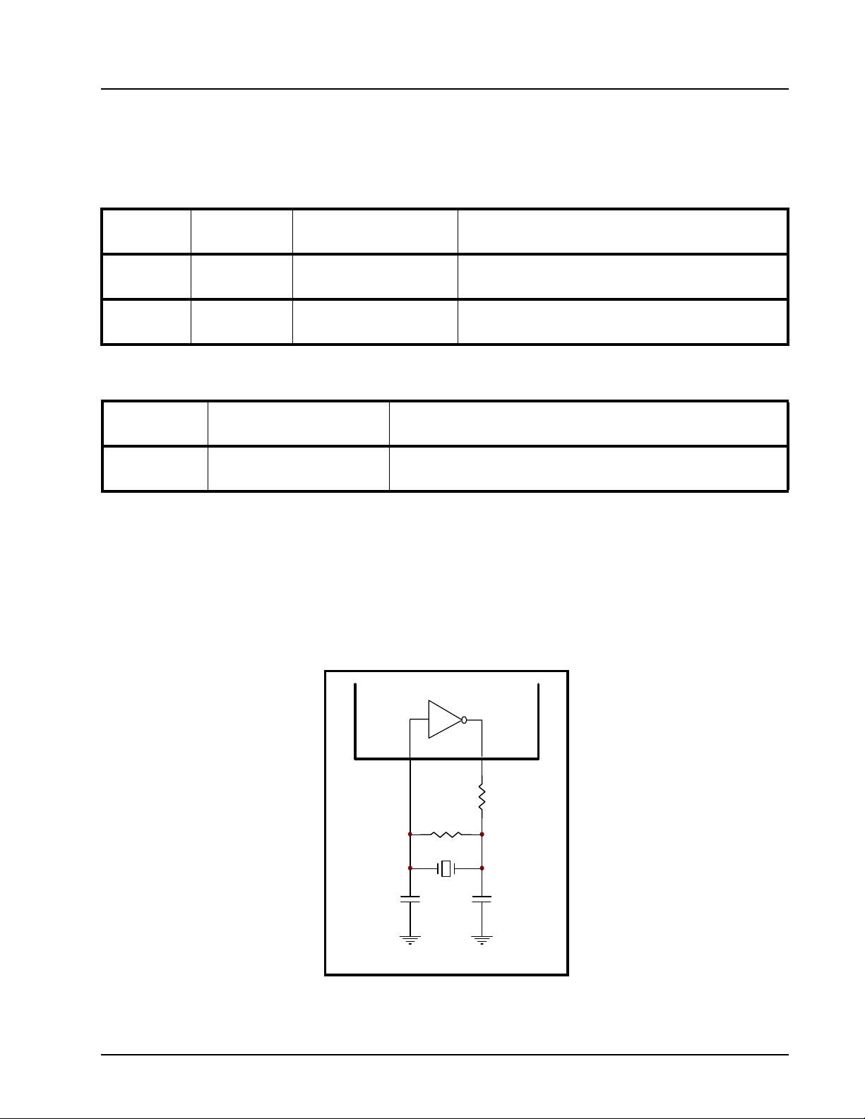
2.10 Crystal Oscillator or External Clock Input
The 2752 includes an on-chip oscillator (XTAL1 and XTAL2) to produce a clock for both UART sections in the
device. The CPU data bus does not require this clock for bus operation. The crystal oscillator provides a
system clock to the Baud Rate Generators (BRG) section found in each of the UART. XTAL1 is the input to the
oscillator or external clock buffer input with XTAL2 pin being the output. For programming details, see
“Programmable Baud Rate Generator.”
FIGURE 4. TYPICAL OSCILLATOR CONNECTIONS
22-47 pF
XTAL1 XTAL2
R2
500 KΩ − 1 MΩ
Y1
C1
C2
22-47 pF
R1
0-120 Ω
(Optional)
1.8432 MHz
to
24 MHz
9
XR16L2752
2.25V TO 5.5V DUART WITH 64-BYTE FIFO
xr
REV. 1.2.0
The on-chip oscillator is designed to use an industry standard microprocessor crystal (parallel resonant,
fundamental frequency with 10-22 pF capacitance load, ESR of 20-120 ohms and 100ppm frequency
tolerance) connected externally between the XTAL1 and XTAL2 pins (see Figure 4). The programmable Baud
Rate Generator is capable of operating with a crystal oscillator frequency of up to 24 MHz. However, with an
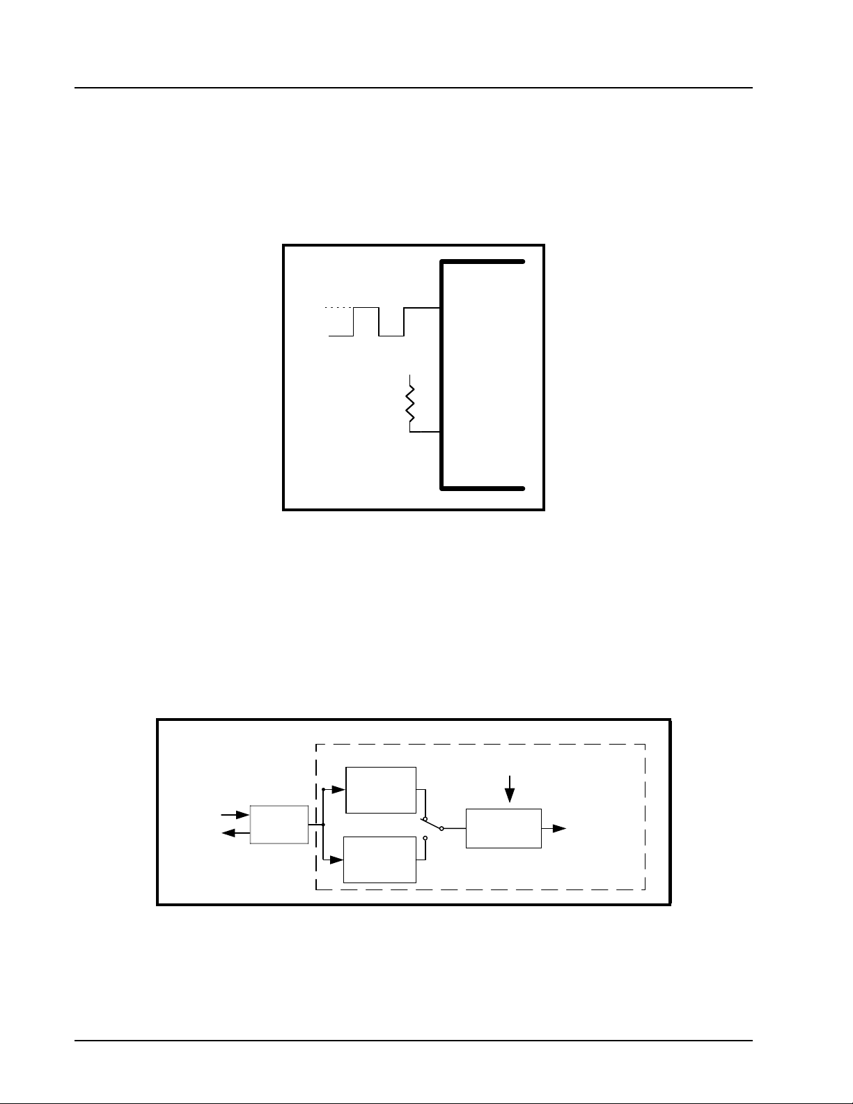
external clock input on XTAL1 pin and a 2K ohms pull-up resistor on XTAL2 pin (as shown in Figure 5) it can
extend its operation up to 50 MHz (6.25 Mbps serial data rate) and 5V with an 8X sampling rate.
F
IGURE 5. EXTERNAL CLOCK CONNECTION FOR EXTENDED DATA RATE
External Clock
vcc
gnd
VCC
R1
2K
XTAL1
XTAL2
For further reading on the oscillator circuit please see the Application Note DAN108 on the EXAR web site at
http://www.exar.com.
2.11 Programmable Baud Rate Generator
Each UART has its own Baud Rate Generator (BRG) with a prescaler. The prescaler is controlled by a
software bit in the MCR register. The MCR register bit-7 sets the prescaler to divide the input crystal or external
clock by 1 or 4. The clock output of the prescaler goes to the BRG. The BRG further divides this clock by a
programmable divisor between 1 and (2
sampling rate clock is used by the transmitter for data bit shifting and
16
-1) to obtain a 16X sampling rate clock of the serial data rate. The
receiver for data sampling. The BRG
divisor defaults to the maximum baud rate (DLL = 0x01 and DLM = 0x00) upon power up.
FIGURE 6. BAUD RATE GENERATOR AND PRESCALER
DLL and DLM
Registers
MCR Bit-7=0
(default)
Baud Rate
Generator
MCR Bit-7=1
Logic
16X
Sam plin g
Rate C loc k to
Transmitter
XTAL1
XTAL2
Prescaler
Divide by 1
Crystal
Osc/
Bu ffer
Prescaler
Divide by 4
Programming the Baud Rate Generator Registers DLM and DLL provides the capability of selecting the
operating data rate. Ta bl e 5 shows the standard data rates available with a 14.7456 MHz crystal or external
clock at 16X sampling rate clock rate. A 16X sampling clock is typically used. However, user can select the 8X
sampling clock rate mode (EMSR bit-7=0) to double the operating data rate. When using a non-standard data
rate crystal or external clock, the divisor value can be calculated for DLL/DLM with the following equation.
10
xr
REV. 1.2.0
divisor (decimal) = (XTAL1 clock frequency / prescaler) / (serial data rate x 16), with 16XMode [EMSR bit-7] = 1
divisor (decimal) = (XTAL1 clock frequency / prescaler) / (serial data rate x 8), with 16XMode [EMSR bit-7] = 0
2.25V TO 5.5V DUART WITH 64-BYTE FIFO
TABLE 5: TYPICAL DATA RATES WITH A 14.7456 MHZ CRYSTAL OR EXTERNAL CLOCK
XR16L2752
O
Data Rate
UTPUT
MCR Bit-7=1
100 400 2304 900 09 00 0
600 2400 384 180 01 80 0
1200 4800 192 C0 00 C0 0
2400 9600 96 60 00 60 0
4800 19.2k 48 30 00 30 0
9600 38.4k 24 18 00 18 0
19.2k 76.8k 12 0C 00 0C 0
38.4k 153.6k 6 06 00 06 0
57.6k 230.4k 4 04 00 04 0
115.2k 460.8k 2 02 00 02 0
230.4k 921.6k 1 01 00 01 0
O
Data Rate
UTPUT
MCR Bit-7=0
(D
EFAULT
D
IVISOR FOR
Clock (Decimal)
)
16x
D
IVISOR FOR
Clock (HEX)
16x
V
ALUE
P
DLM
ROGRAM
(HEX)
DLL
P
V
ALUE
ROGRAM
(HEX)
D
ATA RATE
E
RROR
(%)
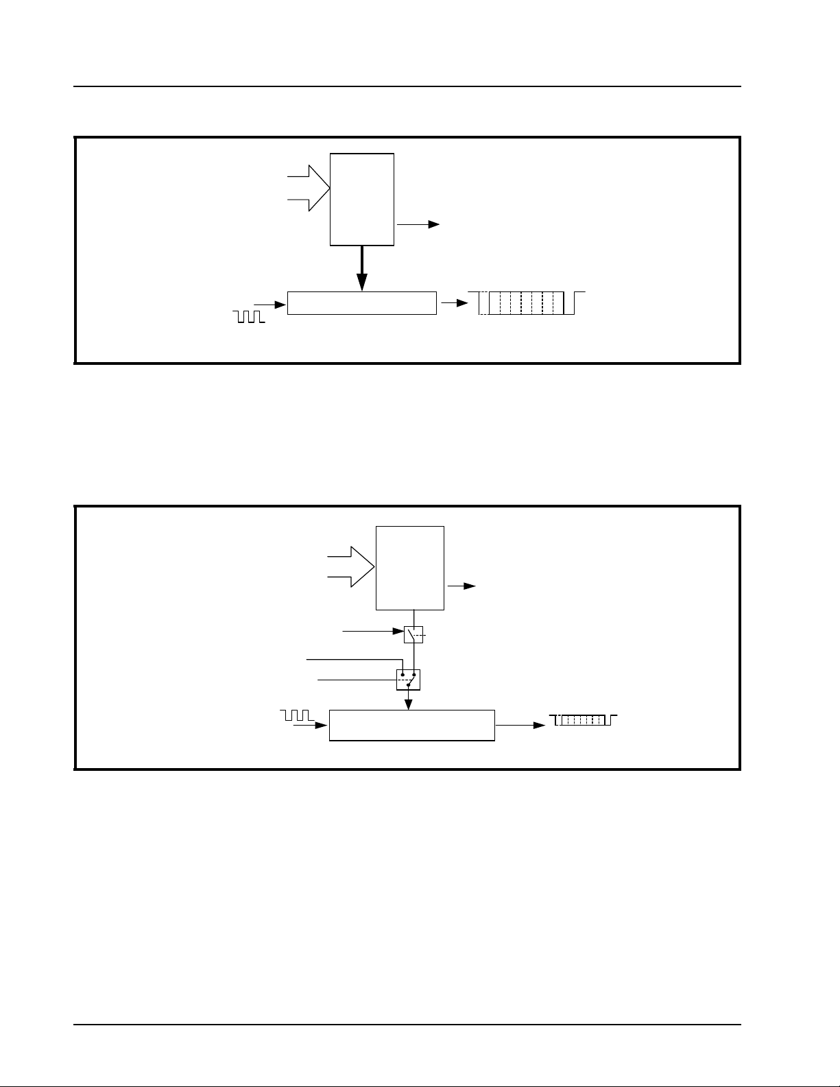
2.12 Transmitter
The transmitter section comprises of an 8-bit Transmit Shift Register (TSR) and 64 bytes of FIFO which
includes a byte-wide Transmit Holding Register (THR). TSR shifts out every data bit with the 16X internal
clock. A bit time is 16 clock periods (see EMSR bit-7). The transmitter sends the start-bit followed by the
number of data bits, inserts the proper parity-bit if enabled, and adds the stop-bit(s). The status of the FIFO
and TSR are reported in the Line Status Register (LSR bit-5 and bit-6).
2.12.1 Transmit Holding Register (THR) - Write Only
The transmit holding register is an 8-bit register providing a data interface to the host processor. The host
writes transmit data byte to the THR to be converted into a serial data stream including start-bit, data bits,
parity-bit and stop-bit(s). The least-significant-bit (Bit-0) becomes first data bit to go out. The THR is the input
register to the transmit FIFO of 64 bytes when FIFO operation is enabled by FCR bit-0. Every time a write
operation is made to the THR, the FIFO data pointer is automatically bumped to the next sequential data
location.
2.12.2 Transmitter Operation in non-FIFO Mode
The host loads transmit data to THR one character at a time. The THR empty flag (LSR bit-5) is set when the
data byte is transferred to TSR. THR flag can generate a transmit empty interrupt (ISR bit-1) when it is enabled
by IER bit-1. The TSR flag (LSR bit-6) is set when TSR becomes completely empty.
11
XR16L2752
2.25V TO 5.5V DUART WITH 64-BYTE FIFO
F
IGURE 7. TRANSMITTER OPERATION IN NON-FIFO MODE
xr
REV. 1.2.0
Data
Byte
16X or 8X Clock
(EMSR bit-7)
Transmit Shift Register (TSR)
Transmit
Holding
Register
(THR)
THR Interrupt (ISR bit-1)
Enabled by IER bit-1
M
S
B
L
S
B
TXNOFIFO1
2.12.3 Transmitter Operation in FIFO Mode
The host may fill the transmit FIFO with up to 64 bytes of transmit data. The THR empty flag (LSR bit-5) is set
whenever the FIFO is empty. The THR empty flag can generate a transmit empty interrupt (ISR bit-1) when the
amount of data in the FIFO falls below its programmed trigger level. The transmit empty interrupt is enabled by
IER bit-1. The TSR flag (LSR bit-6) is set when TSR/FIFO becomes empty.
FIGURE 8. TRANSMITTER OPERATION IN FIFO AND FLOW CONTROL MODE
Transmit
Data Byte
Auto CTS Flow Control (CTS# pin)
Flow Control Characters
(Xoff1/2 and Xon1/2 Reg.
Auto S oftware Flo w C ontrol
Transmit
FIFO
THR Interrupt (ISR bit-1) falls
below the program med Trigger
Level and then when becomes
empty. FIFO is Enabled by FCR
bit-0=1
16X or 8X Clock
(EMSR bit-7 = 1)
Transmit Data Shift Register
(TSR )
TXFIFO1
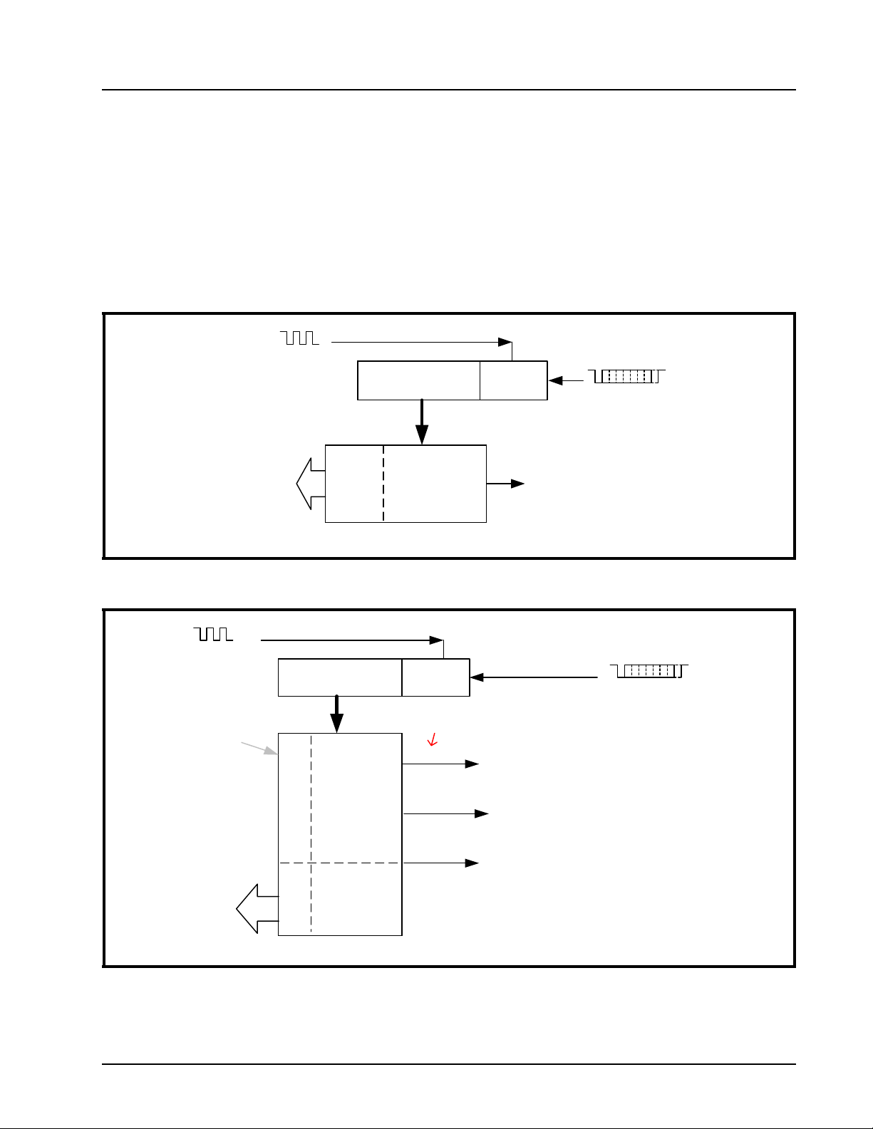
2.13 Receiver
The receiver section contains an 8-bit Receive Shift Register (RSR) and 64 bytes of FIFO which includes a
byte-wide Receive Holding Register (RHR). The RSR uses the 16X for timing. It verifies and validates every bit
on the incoming character in the middle of each data bit. On the falling edge of a start or false start bit, an
internal receiver counter starts counting at the 16X. After 8 clocks the start bit period should be at the center of
the start bit. At this time the start bit is sampled and if it is still a logic 0 it is validated. Evaluating the start bit in
this manner prevents the receiver from assembling a false character. The rest of the data bits and stop bits are
sampled and validated in this same manner to prevent false framing. If there were any error(s), they are
reported in the LSR register bits 2-4. Upon unloading the receive data byte from RHR, the receive FIFO pointer
is bumped and the error tags are immediately updated to reflect the status of the data byte in RHR register.
RHR can generate a receive data ready interrupt upon receiving a character or delay until it reaches the FIFO
trigger level. Furthermore, data delivery to the host is guaranteed by a receive data ready time-out interrupt
12
xr
REV. 1.2.0
XR16L2752
2.25V TO 5.5V DUART WITH 64-BYTE FIFO
when data is not received for 4 word lengths as defined by LCR[1,0] plus 12 bits time. This is equivalent to 3.7-
4.6 character times. The RHR interrupt is enabled by IER bit-0.
2.13.1 Receive Holding Register (RHR) - Read-Only
The Receive Holding Register is an 8-bit register that holds a receive data byte from the Receive Shift
Register. It provides the receive data interface to the host processor. The RHR register is part of the receive
FIFO of 64 bytes by 11-bits wide, the 3 extra bits are for the 3 error tags to be reported in LSR register. When
the FIFO is enabled by FCR bit-0, the RHR contains the first data character received by the FIFO. After the
RHR is read, the next character byte is loaded into the RHR and the errors associated with the current data
byte are immediately updated in the LSR bits 2-4.
FIGURE 9. RECEIVER OPERATION IN NON-FIFO MODE
16X or 8X Clock
(EMSR bit-7)
Receive Data Shift
Register (RSR)
Data Bit
Validation
Receive Data Characters
Receive
Data Byte
and Errors
Error
Tags in
LSR bits
4:2
Receive Data
Holding Register
(RHR)
RHR Interrupt (ISR bit-2)
FIGURE 10. RECEIVER OPERATION IN FIFO AND AUTO RTS FLOW CONTROL MODE
16X or 8X Clock
(EMSR bit-7)
64 bytes by 11-bit
wide
FIFO
Receive Data
Byte and Errors
Receive Data Shift
Register (RSR)
Receive
Data FIFO
(64-sets)
Error Tags
Receive
Data
LSR bits 4:2
Error Tags in
Data Bit
Validation
Example
- RX FIFO trigger level selected at 16
:
Data falls to 8
FIFO Trigger=16
Data fills to 24
bytes
(See No te Below)
RTS# re-asserts when data falls below the flow
control trigger level to restart remote transmitter.
Enable by EFR bit-6=1, MCR bit-2.
RHR Interrupt (ISR bit-2) programmed for
desired FIFO trigger level.
FIFO is Enabled by FCR bit-0=1
RTS# de-asserts when data fills above the flow
control trigger level to suspend remote transmitter.
Enable by EFR bit-6=1, MCR bit-2.
RXFIFO1
Receive Data Characters
RXFIFO1
OTE
Table-B selected as Trigger Table for
N
:
Figure 10 (Table 10 on page 27
13
).

XR16L2752
2.25V TO 5.5V DUART WITH 64-BYTE FIFO
2.14 Auto RTS (Hardware) Flow Control
Automatic RTS hardware flow control is used to prevent data overrun to the local receiver FIFO. The RTS#
output is used to request remote unit to suspend/resume data transmission. The auto RTS flow control
features is enabled to fit specific application requirement (see Figure 11):
Enable auto RTS flow control using EFR bit-6.
•
The auto RTS function must be started by asserting RTS# output pin (MCR bit-1 to logic 1 after it is enabled).
•
If using the Auto RTS interrupt:
Enable RTS interrupt through IER bit-6 (after setting EFR bit-4). The UART issues an interrupt when the
•
RTS# pin makes a transition from low to high: ISR bit-5 will be set to logic 1.
2.15 Auto RTS Hysteresis
The 2752 has a new feature that provides flow control trigger hysteresis while maintaining compatibility with
the XR16C850, ST16C650A and ST16C550 family of UARTs. With the Auto RTS function enabled, an interrupt
is generated when the receive FIFO reaches the programmed RX trigger level. The RTS# pin will not be forced
HIGH (RTS off), until the receive FIFO reaches the upper limit of the hysteresis level. The RTS# pin will return
LOW after the RX FIFO is unloaded to the lower limit of the hysteresis level. Under the above described
conditions, the 2752 will continue to accept data until the receive FIFO gets full. The Auto RTS function is
initiated when the RTS# output pin is asserted LOW (RTS On). Ta b l e 1 3 shows the complete details for the
Auto RTS# Hysteresis levels. Please note that this table is for programmable trigger levels only (Table D). The
hysteresis values for Tables A-C are the next higher and next lower trigger levels in Tables A-C.
2.16 Auto CTS Flow Control
Automatic CTS flow control is used to prevent data overrun to the remote receiver FIFO. The CTS# input is
monitored to suspend/restart the local transmitter. The auto CTS flow control feature is selected to fit specific
application requirement (see Figure 11):
xr
REV. 1.2.0
Enable auto CTS flow control using EFR bit-7.
•
If using the Auto CTS interrupt:
Enable CTS interrupt through IER bit-7 (after setting EFR bit-4). The UART issues an interrupt when the
•
CTS# pin is de-asserted (HIGH): ISR bit-5 will be set to 1, and UART will suspend transmission as soon as
the stop bit of the character in process is shifted out. Transmission is resumed after the CTS# input is reasserted (LOW), indicating more data may be sent.
14

xr
REV. 1.2.0
FIGURE 11. AUTO RTS AND CTS FLOW CONTROL OPERATION
XR16L2752
2.25V TO 5.5V DUART WITH 64-BYTE FIFO
Local UART
Receiver FIFO
Trigger Reached
Auto RTS
Trigger Level
Transmitter
Auto CTS
RTSA#
CTSB#
TXB
RXA FIFO
INTA
(RXA FIFO
Interrupt)
UARTA
Monitor
Data Starts
Assert RTS# to Begin
Transmission
1
2
3
4
Receive
Data
RX FIFO
Trigger Level
RXA TXB
RTSA# CTSB#
RXBTXA
RTSB#CTSA#
ON
ON
5
7
RTS High
Threshold
8
6
OFF
OFF
Suspend
Restart
9
RTS Low
Threshold
10
11
Remote UART
UARTB
Transmitter
Auto CTS
Monitor
Receiver FIFO
Trigger Reached
Auto RTS
Trigger Level
ON
ON
RX FIFO
12
Trigger Level
RTSCTS1
The local UART (UARTA) starts data transfer by asserting RTSA# (1). RTSA# is normally connected to CTSB# (2) of
remote UART (UARTB). CTSB# allows its transmitter to send data (3). TXB data arrives and fills UARTA receive FIFO
(4). When RXA data fills up to its receive FIFO trigger level, UARTA activates its RXA data ready interrupt (5) and continues to receive and put data into its FIFO. If interrupt service latency is long and data is not being unloaded, UARTA
monitors its receive data fill level to match the upper threshold of RTS delay and de-assert RTSA# (6). CTSB# follows
(7) and request UARTB transmitter to suspend data transfer. UARTB stops or finishes sending the data bits in its transmit shift register (8). When receive FIFO data in UARTA is unloaded to match the lower threshold of RTS delay (9),
UARTA re-asserts RTSA# (10), CTSB# recognizes the change (11) and restarts its transmitter and data flow again until
next receive FIFO trigger (12). This same event applies to the reverse direction when UARTA sends data to UARTB
with RTSB# and CTSA# controlling the data flow.
15
 Loading...