

EXAR XR16C854 Service Manual
查询XR16C854供应商
Preliminary
Information
XR16C854
QUAD UART WITH RX/TX FIFO
COUNTERS,128-BYTE FIFO
DESCRIPTION
The XR16C854 *1 (854) is a universal asynchronous receiver and transmitter (UART) with a dual foot print
interface compatible with the ST16C554D/654 and ST68C554/654. The 854 is an enhanced UART with 128 byte
FIFOs, Independent Transmit and Receive FIFO counter, automatic hardware/software flow control, and data
rates up to 1.5Mbps. Onboard status registers provide the user with error indications and operational status,
modem interface control. System interrupts may be tailored to meet user requirements. An internal loop-back
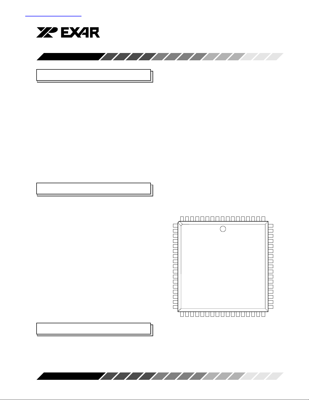
capability allows onboard diagnostics. The 854 is available in 64 pin TQFP, 68 pin PLCC, and 100 pin QFP
packages. The 64 pin package offers the 16 interface mode which is compatible with the industry standard
ST16C554. The 68 and 100 pin packages offer an additional 68 mode which allows easy integration with Motorola,
and other popular microprocessors. The XR16C854CV (64 pin) offers three state interrupt control while the
XR16C854DV provides constant active interrupt outputs. The 64 pin devices do not offer TXRDY/RXRDY outputs
or the default clock select option (CLKSEL). The 100 pin packages offer faster channel status access by providing
separate outputs for TXRDY and RXRDY, offer separate Infrared TX outputs and a musical instrument clock input
(MIDICLK). The 854 combines the package interface modes of the 16C554/654 and 68C554/654 series on a
single integrated chip.
FEATURES
• Compatibility with the Industry Standard
ST16C554/654, ST68C554/654, TL16C554
• 1.5 Mbps transmit/receive operation (24MHz)
• 128 byte transmit and receive FIFO
• Independent transmit and receive FIFO counter
• Automatic software/hardware flow control
• Programmable Xon/Xoff characters
• Software selectable Baud Rate Generator pre-
scaleable clock rates of 1X, 4X.
• Four selectable, and Programmable Transmit/
Receive FIFO interrupt trigger levels
• Standard modem interface or infrared IrDA en-
coder/decoder interface
• Software flow control turned off optionally by any
(Xon) RX character
• Independent MIDI interface on 100 pin packages
• 100 pin packages offer internal register FIFO
monitoring and separate IrDA TX outputs
• Sleep mode ( 200µA stand-by)
ORDERING INFORMATION
-DSRA
-CTSA
-DTRA
VCC
-RTSA
INTA
-CSA
TXA
-IOW
TXB
-CSB
INTB
-RTSB
GND
-DTRB
-CTSB
-DSRB
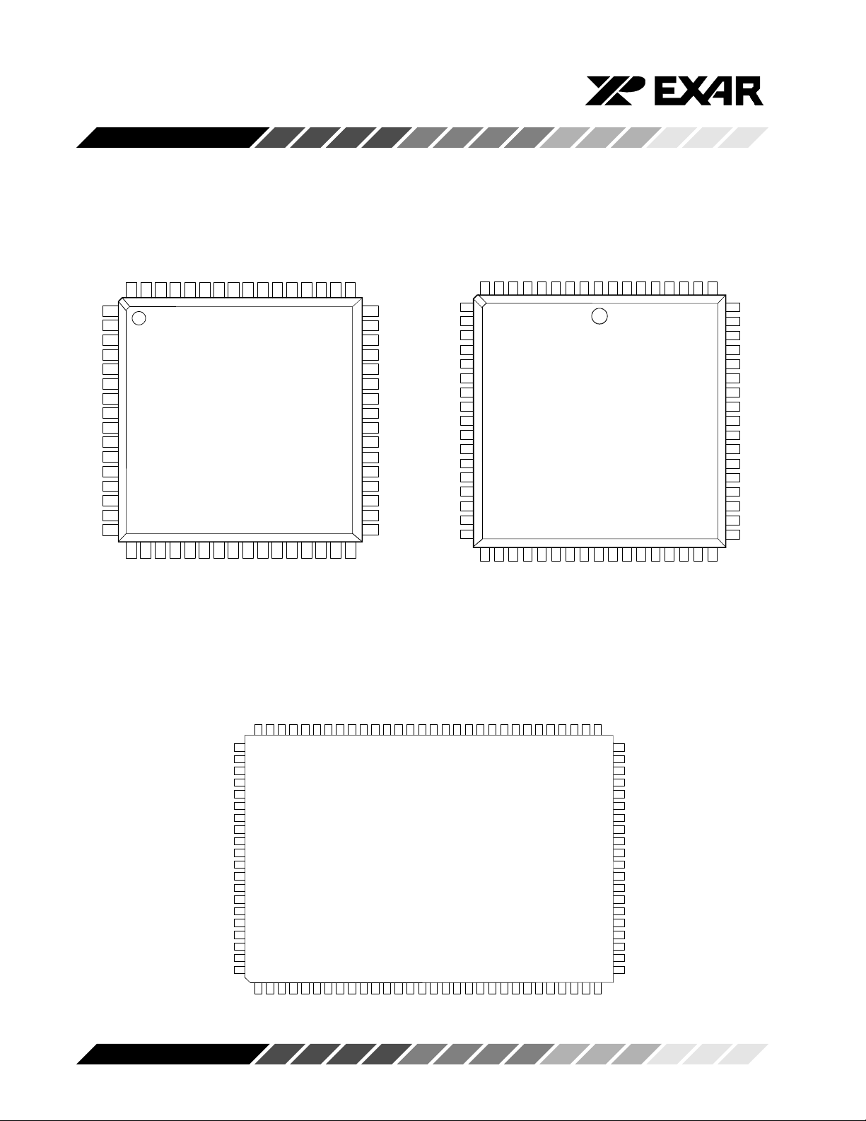
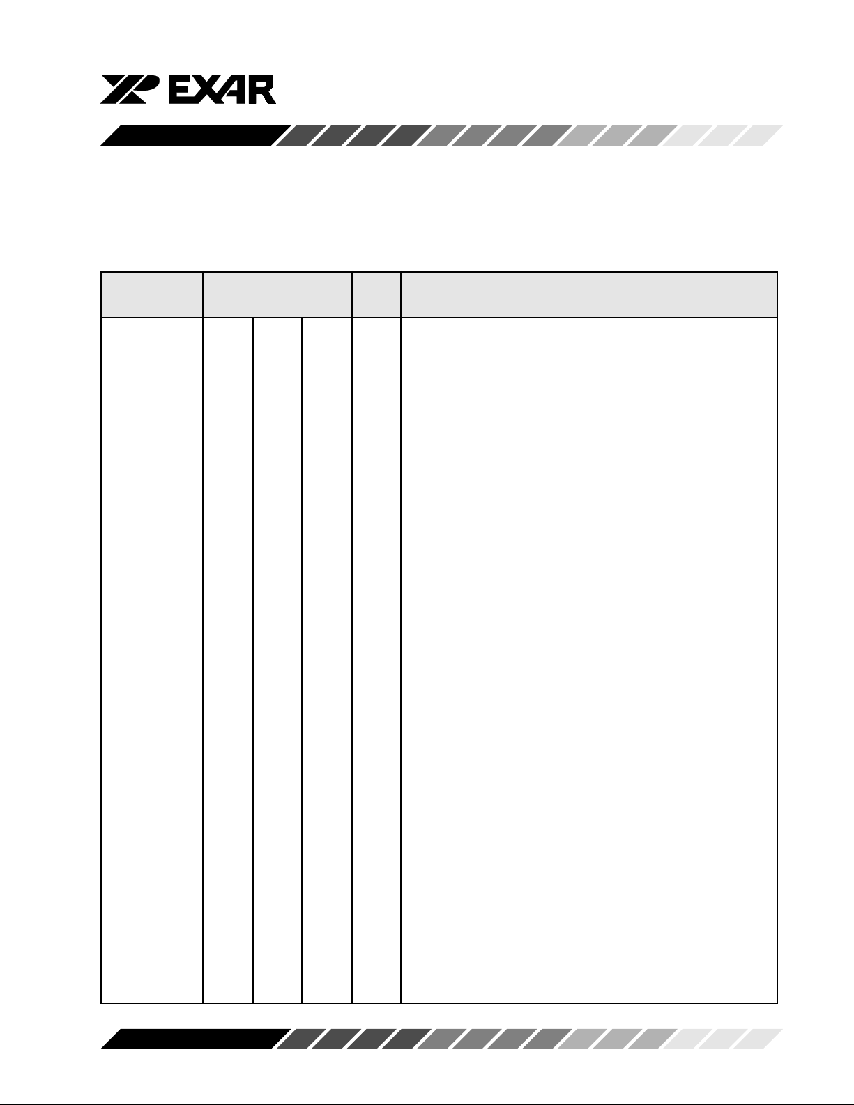
PLCC Package
-CDA
-RIA
RXA
987654321
10
11
12
13
14
15
16
17
18
19
20
21
22
23
24
25
26
2728293031323334353637383940414243
-CDB
GNDD7D6D5D4D3D2D1D0
XR16C854CJ
16 MODE
-RIB
A2A1A0
RXB
16/-68
CLKSEL
68676665646362
XTAL1
XTAL2
INTSEL
RESET
-TXRDY
-RXRDY
VCC
GND
RXD
-RID
-CDD
63
60
-DSRD
59
-CTSD
-DTRD
58
GND
57
-RTSD
56
55
INTD
-CSD
54
TXD
53
-IOR
52
TXC
51
50
-CSC
49
INTC
-RTSC
48
VCC
47
-DTRC
46
45
-CTSC
44
-DSRC
-RIC
RXC
-CDC
Part number Pins Package Operating temperature
XR16C854CJ 68 PLCC 0° C to + 70° C
XR16C854CV 64 TQFP 0° C to + 70° C
XR16C854DCV 64 TQFP 0° C to + 70° C
XR16C854CQ 100 QFP 0° C to + 70° C
Part number Pins Package Operating temperature
XR16C854IJ 68 PLCC -40° C to + 85° C
XR16C854IV 64 TQFP -40° C to + 85° C
XR16C854DIV 64 TQFP -40° C to + 85° C
XR16C854IQ 100 QFP -40° C to + 85° C
Note *1: Patent Pending
Rev. 1.00P
EXAR Corporation, 48720 Kato Road, Fremont, CA 94538 • (510) 668-7000 • FAX (510) 668-7017
XR16C854
Figure 1, Package Descriptions
64 Pin TQFP Package 68 Pin PLCC Package
-CDA
-RIA
RXA
GNDD7D6D5D4D3D2D1D0
646362616059585756555453525150
1
-DSRA
2
-CTSA
3
-DTRA
4
VCC
5
-RTSA
6
INTA
7
-CSA
8
TXA
-IOW
-TXB
-CSB
INTB
-RTSB
GND
-DTRB
-CTSB
9
10
11
12
13
14
15
16
171819202122232425262728293031
-CDB
-DSRB
XR16C854CV
XR16C854DCV
RXB
VCC
A2A1A0
-RIB
XTAL1
XTAL2
VCC
RXD
-RID
-CDD
49
-DSRD
48
-CTSD
47
-DTRD
46
GND
45
-RTSD
44
INTD
43
-CSD
42
TXD
41
-IOR
40
TXC
39
-CSC
38
INTC
37
-RTSC
36
VCC
35
-DTRC
34
-CTSC
33
-DSRA
-CTSA
-DTRA
VCC
-RTSA
-IRQ
TXA
R/-W
TXB
N.C.
-RTSB
GND
-DTRB
-CTSB
32
-RIC
RXC
GND
RESET
-CDC
-DSRC
-CDA-RIA
RXA
GNDD7D6D5D4D3D2D1D0
987654321
10
11
12
13
14
15
16
-CS
17
18
19
20
A3
XR16C854CJ
68 MODE
21
22
23
24
25
272829303132333435363738394041
-RIB
RXB
-CDB
A2A1A0
16/-68
CLKSEL
68676665646362
N.C.
XTAL1
XTAL2
-RESET
-TXRDY
-RXRDY
VCC
GND
RXD
-RID
-DSRD
60
59
-CTSD
-DTRD
58
GND
57
-RTSD
56
55
N.C.
54
N.C.
TXD
53
N.C.
52
TXC
51
A4
50
49
N.C.
-RTSC
48
VCC
47
-DTRC
46
45
-CTSC
42
-RIC
RXC
Rev. 1.00P
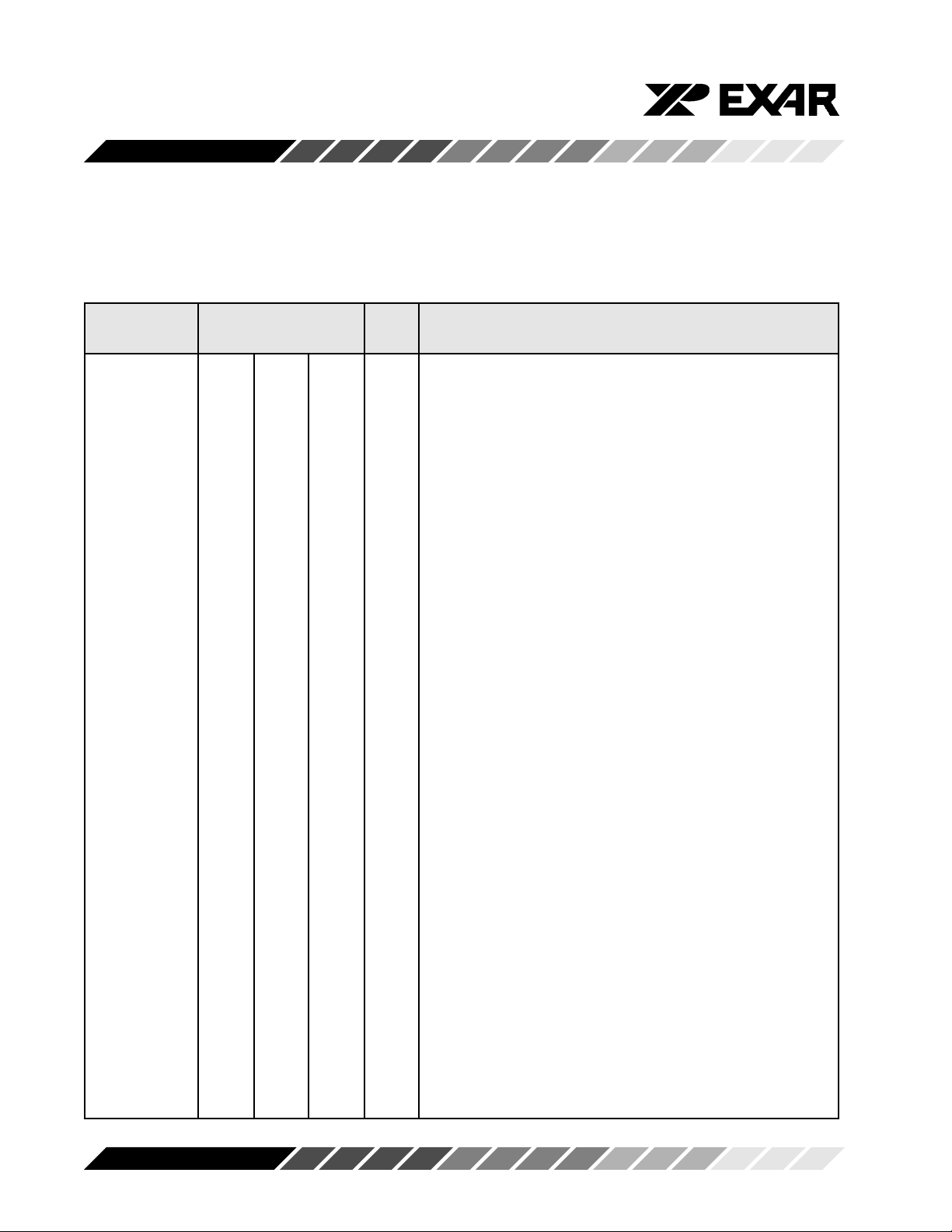
100 Pin QFP Package
N.C.
N.C.
N.C.
N.C.
-CSRDY
IRTXD
-DSRD
-CTSD
-DTRD
GND
-RTSD
INTD
-CSD
TXD
-IOR
TXC
-CSC
INTC
-RTSC
VCC
-DTRC
-CTSC
8079787776757473727170696867666564636261605958575655545352
81
-TXRDYD
82
-RXRDYD
83
-CDD
84
-RID
85
RXD
86
VCC
87
INTSEL
88
D0
89
D1
90
D2
91
D3
92
D4
93
D5
94
D6
95
D7
96
GND
97
RXA
98
-RIA
99
-CDA
100
-RXRDYA
123456789
N.C.
N.C.
N.C.
N.C.
IRTXA
-CTSA
-DSRA
-TXRDYA
XR16C854CQ
101112131415161718192021222324252627282930
TXA
VCC
INTA
-RTSA
-DTRA
TXB
INTB
-IOW
-CSA
-CSB
-RTSB
-DSRC
GND
-CTSB
-DTRB
-DSRB
IRTXC
-TXRDYC
N.C.
N.C.
N.C.
N.C.
N.C.
51
N.C.
N.C.
N.C.
N.C.
IRTXB
-TXRDYB
N.C.
-RXRDYC
50
-CDC
49
-RIC
48
RXC
47
GND
46
-TXRDY
45
-RXRDY
44
RESET
43
MIDICLK
42
XTAL2
41
XTAL1
40
A0
39
A1
38
A2
37
16/-68
36
CLKSEL
35
RXB
34
-RIB
33
-CDB
32
-RXRDYB
31
2
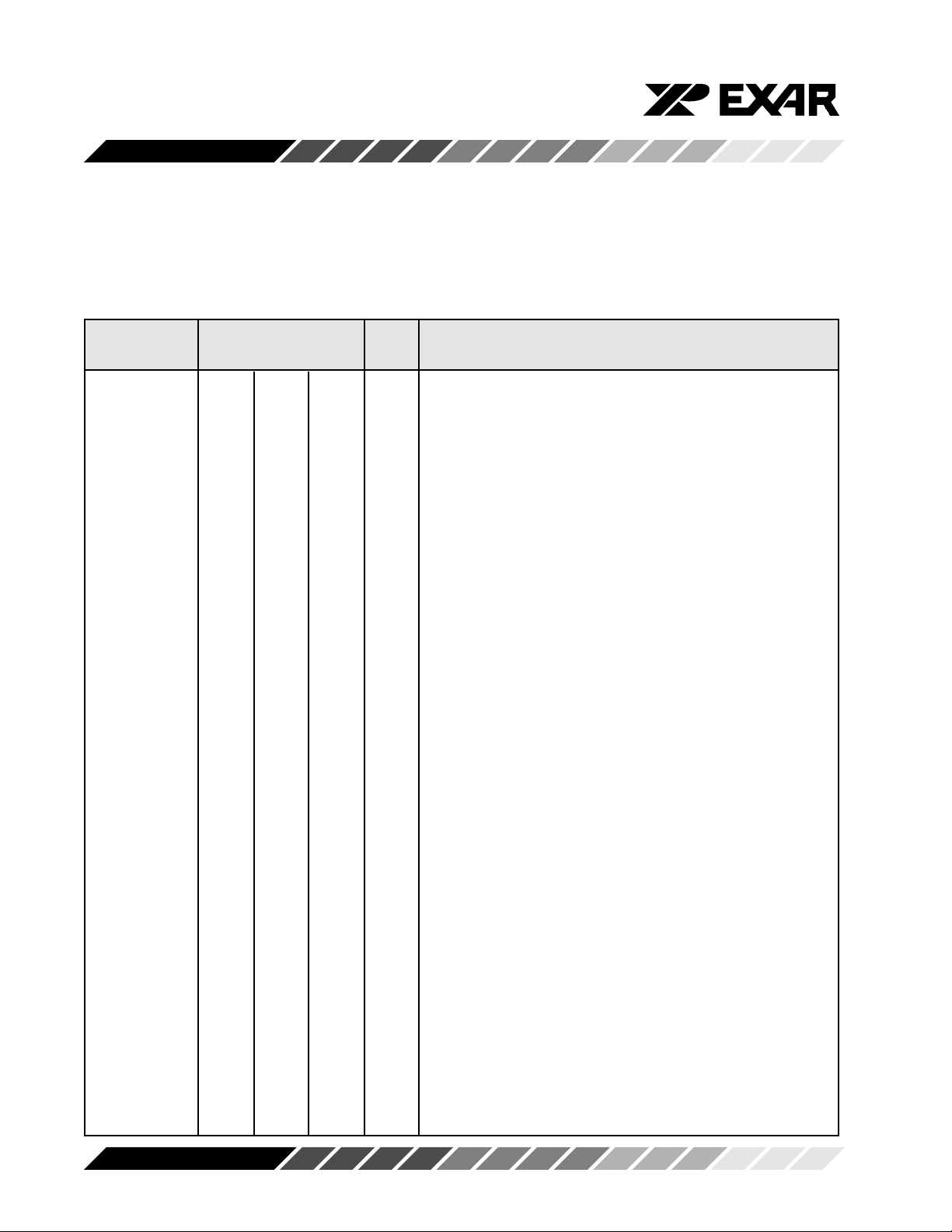
Figure 2, Block Diagram 16 Mode
XR16C854
D0-D7
-IOR
-IOW
RESET
A0-A2
-CS A-D
INT A-D
-RXRDY A-D
-TXRDY A-D
INTSEL
&
Data bus
Select
Register
Control
Interrupt
Control Logic
Logic
Logic
Transmit
FIFO
Registers
Flow
Control
Logic
Receive
FIFO
Registers
&
Flow
Control signals
Inter Connect Bus Lines
Control
Logic
Transmit
Shift
Register
Receive
Shift
Register
TX A-D
Ir
Encoder
RX A-D
RXIR A-D
Ir
Decoder
-DTR A-D
-RTS A-D
XTAL1
MIDI
XTAL2
Rev. 1.00P
&
Clock
Modem
Control
Logic
Generator
Baud Rate
3
-CTS A-D
-RI A-D
-CD A-D
-DSR A-D
XR16C854
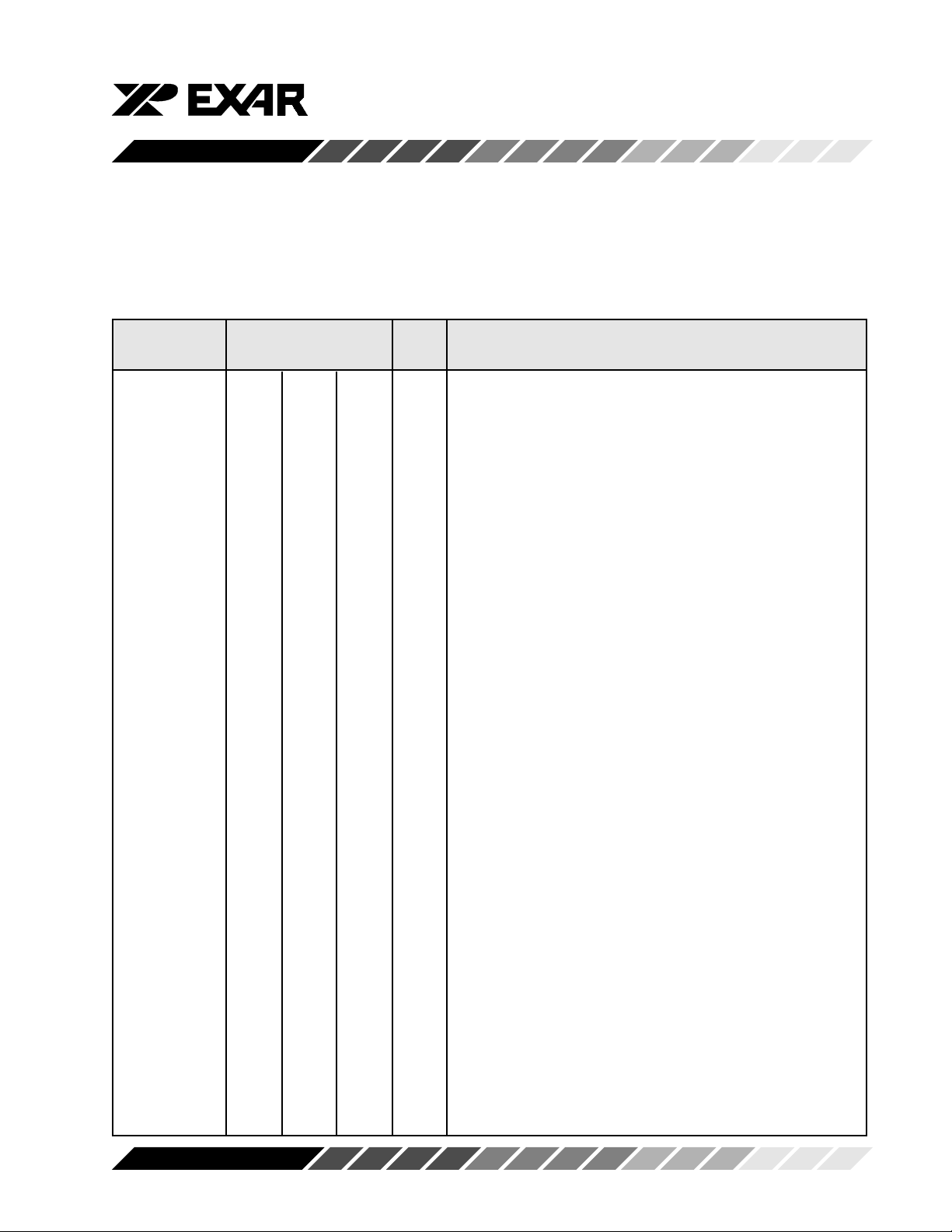
Figure 3, Block Diagram 68 Mode
D0-D7
R/-W
-RESET
A0-A4
-CS
IRQ
-RXRDY A-D
-TXRDY A-D
Data bus
Register
Interrupt
&
Select
Control
Control Logic
Logic
Logic
Transmit
FIFO
Registers
Flow
Control
Logic
Receive
FIFO
Registers
&
Flow
Control signals
Inter Connect Bus Lines
Control
Logic
Transmit
Shift
Register
Receive
Shift
Register
TX A-D
Ir
Encoder
RX A-D
RXIR A-D
Ir
Decoder
-DTR A-D
-RTS A-D
XTAL1
MIDI
XTAL2
Rev. 1.00P
&
Clock
Generator
Baud Rate
Modem
Control
Logic
4
-CTS A-D
-RI A-D
-CD A-D
-DSR A-D
XR16C854
SYMBOL DESCRIPTION
Symbol Pin Signal Pin Description
68 100 64 type
16/-68 31 36 - I 16/68 Interface Type Select (input with internal pull-up). -
This input provides the 16 (Intel) or 68 (Motorola) bus
interface type select. The functions of -IOR, -IOW, INT AD, and -CS A-D are re-assigned with the logical state of this
pin. When this pin is a logic 1, the 16 mode interface 16C554
is selected. When this pin is a logic 0, the 68 mode interface
(68C554) is selected. When this pin is a logic 0, -IOW is reassigned to R/-W, RESET is re-assigned to -RESET, -IOR
is not used, and INT A-D(s) are connected in a WIRE-OR
configuration. The WIRE-OR outputs are connected internally to the open source IRQ signal output. This pin is not
available on 64 pin packages which operate in the 16 mode
only.
A0 34 39 24 I Address-0 Select Bit. Internal registers address selection in
16 and 68 modes.
A1 33 38 23 I Address-1 Select Bit. Internal registers address selection in
16 and 68 modes.
A2 32 37 22 I Address-2 Select Bit. - Internal registers address selection
in 16 and 68 modes.
A3-A4 20,50 17,64 - I Address 3-4 Select Bits. - When the 68 mode is selected,
these pins are used to address or select individual UARTs
(providing -CS is a logic 0). In the 16 mode, these pins are
reassigned as chip selects, see -CSB and -CSC. These pins
are not available on 64 pin packages which operate in the
16 mode only.
CLKSEL 30 35 - I Clock Select. - The 1X or 4X pre-scaleable clock is selected
by this pin. The 1X clock is selected when CLKSEL is a logic
1 (connected to VCC) or the 4X is selected when CLKSEL
is a logic 0 (connected to GND). MCR bit-7 can override the
state of this pin following reset or initialization (see MCR bit-
7). This pin is not available on 64 pin packages which
provide MCR bit-7 selection only.
-CS 16 13 - I Chip Select. (active low) - In the 68 mode, this pin functions
as a multiple channel chip enable. In this case, all four
Rev. 1.00P
5
XR16C854
SYMBOL DESCRIPTION
Symbol Pin Signal Pin Description
68 100 64 type
UARTs (A-D) are enabled when the -CS pin is a logic 0. An
individual UART channel is selected by the data contents of
address bits A3-A4. When the 16 mode is selected (68/100
pin devices), this pin functions as -CSA, see definition under
-CS A-B. This pin is not available on 64 pin packages which
operate in the 16 mode only.
-CS A-B 16,20 13,17 7,11
-CS C-D 50,54 64,68 38,42 I Chip Select A, B, C, D (active low) - This function is
associated with the 16 mode only, and for individual channels, A through D. When in 16 Mode, these pins enable
data transfers between the user CPU and the XR16C854 for
the channel(s) addressed. Individual UART sections (A, B,
C, D) are addressed by providing a logic 0 on the respective
-CS A-D pin. When the 68 mode is selected, the functions
of these pins are reassigned. 68 mode functions are described under the their respective name/pin headings.
-CSRDY - 76 - I Control Status Ready (active low) - This feature is available
on 100 pin QFP packages only. On 100 pin packages, the
Contents of the FIFORDY Register is read when this pin is
a logic 0. However it should be noted, D0-D3 will contain the
inverted logic states of TXRDY, status bits A-D, and D4-D7
the inverted logic states of RXRDY, status bits D4-D7.
D0-D2 66-68 88-90 53-55 I/O
D3-D7 1-5 91-95 56-60 Data Bus (Bi-directional) - These pins are the eight bit, three
state data bus for transferring information to or from the
controlling CPU. D0 is the least significant bit and the first
data bit in a transmit or receive serial data stream.
GND 6,23 96,20 14,28
GND 40,57 46,71 45,61 Pwr Signal and power ground.
INT A-B 15,21 12,18 6,12
INT C-D 49,55 63,69 37,43 O Interrupt A, B, C, D (active high) - This function is associated
with the 16 mode only. These pins provide individual
channel interrupts, INT A-D. INT A-D are enabled when
MCR bit-3 is set to a logic 1, interrupts are enabled in the
interrupt enable register (IER), and when an interrupt con-
Rev. 1.00P
6

XR16C854
SYMBOL DESCRIPTION
Symbol Pin Signal Pin Description
68 100 64 type
dition exists. Interrupt conditions include: receiver errors,
available receiver buffer data, transmit buffer empty, or
when a modem status flag is detected. When the 68 mode
is selected, the functions of these pins are reassigned. 68
mode functions are described under the their respective
name/pin headings.
INTSEL 65 87 - I Interrupt Select. (active high, with internal pull-down) - This
function is associated with the 16 mode only. When the 16
mode is selected, this pin can be used in conjunction with
MCR bit-3 to enable or disable the three state interrupts, INT
A-D or override MCR bit-3 and force continuous interrupts.
Interrupt outputs are enabled continuously by making this
pin a logic 1. Making this pin a logic 0 allows MCR bit-3 to
control the three state interrupt output. In this mode, MCR
bit-3 is set to a logic 1 to enable the three state outputs.
This pin is disabled in the 68 mode. Due to pin limitations on
64 pin packages, this pin is not available. To cover this
limitation, two 64 pin QFP package versions are offered.
The XR16C854DCV operates in the continuos interrupt
enable mode by bonded this pin to VCC internally. The
XR16C854CV operates with MCR bit-3 control by bonding
this pin to GND.
-IOR 52 66 40 I Input/Output Read. (active low Strobe) - This function is
associated with the 16 mode only. A logic 0 transition on this
pin will load the contents of an Internal register defined by
address bits A0-A2 onto the XR16C854 data bus (D0-D7)
for access by an external CPU. This pin is disabled in the 68
mode.
-IOW 18 15 9 I Input/Output Write. (active low strobe) - This function is
associated with the 16 mode only. A logic 0 transition on this
pin will transfer the contents of the data bus (D0-D7) from
the external CPU to an internal register that is defined by
address bits A0/A2. When the 16 mode is selected (68/100
pin devices), this pin functions as R/-W, see definition under
R/W.
Rev. 1.00P
7

XR16C854
SYMBOL DESCRIPTION
Symbol Pin Signal Pin Description
68 100 64 type
-IRQ 15 12 - O Interrupt Request or Interrupt A - This function is associated with the 68 mode only. In the 68 mode, interrupts from
UART channels A-D are WIRE-ORed internally to function
as a single IRQ interrupt. This pin transitions to a logic 0 (if
enabled by the interrupt enable register) whenever a UART
channel(s) requires service. Individual channel interrupt
status can be determined by addressing each channel
through its associated internal register, using -CS and A3A4. In the 68 mode an external pull-up resistor must be
connected between this pin and Vcc. The function of this pin
changes to INTA when operating in the 16 mode, see
definition under INTA.
IRTX A-B - 6,24 IRTX C-D - 57,75 - O Infrared Transmit Data Output (IrDA) - This function is
associated with 100 pin packages only. These pins provide
separate infrared IrDA TX outputs for UART channels (AD). The serial infrared IRTX data is transmitted via these
pins with added start, stop and parity bits. The IRTX signal
will be a logic 0 during reset, idle (no data), or when the
transmitter is disabled. MCR bit-6 selects the standard
modem or infrared interface.
MIDICLK - 42 - I MIDI (Musical Instrument Digital Interface) Clock Input -
This function is associated with 100 pin packages only. RXC
and TXC can function as MIDI input/output ports when an
external MIDI Clock is provided at this pin. External Clock
or a crystal is connected to the XTAL2 pins for normal
operation (see XTAL 1 & 2).
-RESET
RESET 37 43 27 I Reset. - In the 16 mode a logic 1 on this pin will reset the
internal registers and all the outputs. The UART transmitter
output and the receiver input will be disabled during reset
time. (See XR16C854 External Reset Conditions for initialization details.) When 16/-68 is a logic 0 (68 mode), this pin
functions similarly but, as an inverted reset interface signal,
-RESET.
Rev. 1.00P
8

XR16C854
SYMBOL DESCRIPTION
Symbol Pin Signal Pin Description
68 100 64 type
R/-W 18 15 - I Read/Write Strobe (active low) - This function is associated
with the 68 mode only. This pin provides the combined
functions for Read or Write strobes. A logic 1 to 0 transition
transfers the contents of the CPU data bus (D0-D7) to the
register selected by -CS and A0-A4. Similarly a logic 0 to 1
transition places the contents of a 854 register selected by
-CS and A0-A4 on the data bus, D0-D7, for transfer to an
external CPU.
-RXRDY 38 44 - O Receive Ready (active low) - This function is associated
with 68 and 100 pin packages only. -RXRDY contains the
wire OR-ed status of all four receive channel FIFOs,
RXRDY A-D. A logic 0 indicates receive data ready status,
i.e. the RHR is full or the FIFO has one or more RX
characters available for unloading. This pin goes to a logic
1 when the FIFO/RHR is full or when there are no more
characters available in either the FIFO or RHR. The 100 pin
chip-sets provide both the combined wire ored output and
individual channel RXRDY-A-D outputs. RXRDY A-D is
discussed in a following paragraph. For 64/68 pin packages,
individual channel RX status is read by examining individual internal registers via -CS and A0-A4 pin functions.
-RXRDY A-B - 100,31
-RXRDY C-D - 50,82 - O Receive Ready A-D (active low) - This function is associated with 100 pin packages only. This function provides the
RX FIFO/RHR status for individual receive channels (A-D).
A logic 0 indicates there is receive data to read/unload, i.e.,
receive ready status with one or more RX characters
available in the FIFO/RHR. This pin is a logic 1 when the
FIFO/RHR is empty or when the programmed trigger level
has not been reached.
-TXRDY 39 45 - O (active low) - This function is associated with 68 and 100 pin
packages only. -TXRDY contains the wire OR-ed status of
all four transmit channel FIFOs, TXRDY A-D. A logic 0
indicates a buffer ready status, i.e., at least one location is
empty and available in one of the TX channels (A-D). This
pin goes to a logic 1 when all four channels have no more
empty locations in the TX FIFO or THR. The 100 pin chip-
Rev. 1.00P
9
XR16C854
SYMBOL DESCRIPTION
Symbol Pin Signal Pin Description
68 100 64 type
sets provide both the combined wire ored output and
individual channel TXRDY-A-D outputs. TXRDY A-D is
discussed in a following paragraph For 64/68 pin packages,
individual channel TX status can be read by examining
individual internal registers via -CS and A0-A4 pin functions.
-TXRDY A-B - 5,25
-TXRDY C-D - 56,81 - O This function is associated with 100 pin packages only.
These outputs provide the TX FIFO/THR status for individual transmit channels (A-D). As such, an individual
channels -TXRDY A-D buffer ready status is indicated by
logic 0, i.e., at least one location is empty and available in
the FIFO or THR. This pin goes to a logic 1 when there are
no more empty locations in the FIFO or THR.
VCC 13 10 4,21
VCC 47,64 61,86 35,52 I Power supply inputs.
XTAL1 35 40 25 I Crystal or External Clock Input - Functions as a crystal input
or as an external clock input. A crystal can be connected
between this pin and XTAL2 to form an internal oscillator
circuit (see figure 8). Alternatively, an external clock can be
connected to this pin to provide custom data rates (see
Baud Rate Generator Programming and optional MIDCLK).
XTAL2 36 41 26 O Output of the Crystal Oscillator or Buffered Clock - (See also
XTAL1). Crystal oscillator output or buffered clock output.
-CD A-B 9,27 99,32 64,18
-CD C-D 43,61 49,83 31,49 I Carrier Detect (active low) - These inputs are associated
with individual UART channels A through D. A logic 0 on this
pin indicates that a carrier has been detected by the modem
for that channel.
-CTS A-B 11,25 8,22 2,16
-CTS C-D 45,59 59,73 33,47 I Clear to Send (active low) - These inputs are associated with
individual UART channels, A through D. A logic 0 on the CTS pin indicates the modem or data set is ready to accept
transmit data from the 854. Status can be tested by reading
Rev. 1.00P
10
XR16C854
SYMBOL DESCRIPTION
Symbol Pin Signal Pin Description
68 100 64 type
MSR bit-4. This pin only affects the transmit and receive
operations when Auto CTS function is enabled via the
Enhanced Feature Register (EFR) bit-7, for hardware flow
control operation.
-DSR A-B 10,26 7,23 1,17
-DSR C-D 44,60 58,74 32,48 I Data Set Ready (active low) - These inputs are associated
with individual UART channels, A through D. A logic 0 on
this pin indicates the modem or data set is powered-on and
is ready for data exchange with the UART. This pin has no
effect on the UARTs transmit or receive operation.
-DTR A-B 12,24 9,21 3,15
-DTR C-D 46,58 60,72 34,46 O Data Terminal Ready (active low) - These inputs are
associated with individual UART channels, A through D. A
logic 0 on this pin indicates that the 854 is powered-on and
ready. This pin can be controlled via the modem control
register. Writing a logic 1 to MCR bit-0 will set the -DTR
output to logic 0, enabling the modem. This pin will be a logic
1 after writing a logic 0 to MCR bit-0, or after a reset. This
pin has no effect on the UARTs transmit or receive operation.
-RI A-B 8,28 98,33 63,19
-RI C-D 42,62 48,84 30,50 I Ring Indicator (active low) - These inputs are associated
with individual UART channels, A through D. A logic 0 on
this pin indicates the modem has received a ringing signal
from the telephone line. A logic 1 transition on this input pin
will generate an interrupt.
-RTS A-B 14,22 11,19 5,13
-RTS C-D 48,56 62,70 36,44 O Request to Send (active low) - These outputs are associated
with individual UART channels, A through D. A logic 0 on the
-RTS pin indicates the transmitter has data ready and
waiting to send. Writing a logic 1 in the modem control
register (MCR bit-1) will set this pin to a logic 0 indicating
data is available. After a reset this pin will be set to a logic
1. This pin only affects the transmit and receive operations
when Auto RTS function is enabled via the Enhanced
Feature Register (EFR) bit-6, for hardware flow control
Rev. 1.00P
11
XR16C854
SYMBOL DESCRIPTION
Symbol Pin Signal Pin Description
68 100 64 type
operation.
RX/IRRX A-B 7,29 97,34 62,20
RX/IRRX C-D 41,63 47,85 29,51 I Receive Data Input RX/IRRX A-D. - These inputs are
associated with individual serial channel data to the
XR16C854. Two user selectable interface options are avail-
able. The first option supports the standard modem inter-
face. The second option provides an Infrared decoder
interface, see figures 2/3. When using the standard modem
interface, the RX signal will be a logic 1 during reset, idle (no
data), or when the transmitter is disabled. The inactive state
(no data) for the Infrared decoder interface is a logic 0. MCR
bit-6 selects the standard modem or infrared interface.
During the local loop-back mode, the RX input pin is
disabled and TX data is internally connected to the UART
RX Input, internally.
TX/IRTX A-B 17,19 14,16 8,10
TX/IRTX C-D 51,53 65,67 39,41 O Transmit Data - These outputs are associated with indi-
vidual serial transmit channel data from the 854. Two user
selectable interface options are available. The first user
option supports a standard modem interface. The second
option provides an Infrared encoder interface, see figures 2/
3. When using the standard modem interface, the TX signal
will be a logic 1 during reset, idle (no data), or when the
transmitter is disabled. The inactive state (no data) for the
Infrared encoder/ decoder interface is a Logic 0. MCR bit-
6 selects the standard modem or infrared interface. During
the local loop-back mode, the TX input pin is disabled and
TX data is internally connected to the UART RX Input.
Rev. 1.00P
12

XR16C854
GENERAL DESCRIPTION
The 854 provides serial asynchronous receive data
synchronization, parallel-to-serial and serial-to-parallel data conversions for both the transmitter and
receiver sections. These functions are necessary for
converting the serial data stream into parallel data that
is required with digital data systems. Synchronization
for the serial data stream is accomplished by adding
start and stops bits to the transmit data to form a data
character (character orientated protocol). Data integrity is insured by attaching a parity bit to the data
character. The parity bit is checked by the receiver for
any transmission bit errors. The electronic circuitry to
provide all these functions is fairly complex especially
when manufactured on a single integrated silicon
chip. The XR16C854 represents such an integration
with greatly enhanced features. The 854 is fabricated
with an advanced CMOS process to achieve low drain
power and high speed requirements.
The 854 is an upward solution that provides 128 bytes
of transmit and receive FIFO memory, instead of 64
bytes provided in ST16C654, 16 bytes provided in the
16/68C554, or none in the 16/68C454. The 854 is
designed to work with high speed modems and shared
network environments, that require fast data processing time. Increased performance is realized in the 854
by the larger transmit and receive FIFOs. This allows
the external processor to handle more networking
tasks within a given time. For example, the ST16C554
with a 16 byte FIFO, unloads 16 bytes of receive data
in 1.53 ms (This example uses a character length of 11
bits, including start/stop bits at 115.2Kbps). This
means the external CPU will have to service the
receive FIFO at 1.53 ms intervals. However with the
128 byte FIFO in the 854, the data buffer will not
require unloading/loading for 12.2 ms. This increases
the service interval giving the external CPU additional
time for other applications and reducing the overall
UART interrupt servicing time. In addition, the 4
selectable levels of FIFO trigger interrupt and automatic hardware/software flow control is uniquely provided for maximum data throughput performance
especially when operating in a multi-channel environment. The combination of the above greatly reduces
the bandwidth requirement of the external controlling
CPU, increases performance, and reduces power
consumption.
The 854 combines the package interface modes of the
16C554/654 and 68/C554/654 series on a single integrated chip. The 16 mode interface is designed to
operate with the Intel type of microprocessor bus while
the 68 mode is intended to operate with Motorola, and
other popular microprocessors. Following a reset, the
854 is down-ward compatible with the ST16C454/
ST68C454 or the ST68C454/ST68C554 dependent
on the state of the interface mode selection pin, 16/-
68.
The 854 is capable of operation to 1.5Mbps with a 24
MHz crystal or external clock input. With a crystal of
14.7464 MHz and through a software option, the user
can select data rates up to 460.8Kbps or 921.6Kbps,
8 times faster than the 16C554.
The rich feature set of the 854 is available through
internal registers. Automatic hardware/software flow
control, selectable transmit and receive FIFO trigger
levels, selectable TX and RX baud rates, infrared
encoder/decoder interface, modem interface controls, and a sleep mode are all standard features. MCR
bit-5 provides a facility for turning off (Xon) software
flow control with any incoming (RX) character. In the
16 mode INTSEL and MCR bit-3 can be configured to
provide a software controlled or continuous interrupt
capability. Due of pin limitations for the 64 pin 854 this
feature is offered by two different QFP packages. The
XR16C854DCV operates in the continuos interrupt
enable mode by bonded INTSEL to VCC internally.
The XR16C854CV operates in conjunction with MCR
bit-3 by bonding INTSEL to GND internally.
The 68 and 100 pin XR16C854 packages offer a clock
select pin to allow system/board designers to preset
the default baud rate table. The CLKSEL pin selects
the 1X or 4X pre-scaleable baud rate generator table
during initialization, but can be overridden following
initialization by MCR bit-7.
The 100 pin packages offer several enhances features. These features include an MIDI clock input, an
internal FIFO monitor register, and separate IrDA TX
outputs. The MIDI (Musical Instrument Digital Interface) can be connected to the XTAL2 pin for normal
Rev. 1.00P
13
XR16C854
operation or to external MIDI oscillator for MIDI applications. A separate register is provided for monitoring
the real time status of the FIFO signals -TXRDY and
-RXRDY for each of the four UART channels (A-D).
This reduces polling time involved in accessing individual channels. The 100 pin QFP package also
offers, four separate IrDA (Infrared Data Association
Standard) outputs for Infrared applications. These
outputs are provided in addition to the standard asynchronous modem data outputs.
FUNCTIONAL DESCRIPTIONS
Interface Options
Two user interface modes are selectable for the 854
package. These interface modes are designated as
the 16 mode and the 68 mode. This nomenclature
corresponds to the early 16C554/654 and 68C554/
654 package interfaces respectively.
The 16 Mode Interface
The 16 mode configures the package interface pins for
connection as a standard 16 series (Intel) device and
operates similar to the standard CPU interface available on the 16C554/654. In the 16 mode (pin 16/-68
logic 1) each UART is selected with individual chip
select (CSx) pins as shown in Table 2 below.
Table 2, SERIAL PORT CHANNEL SELECTION
GUIDE, 16 MODE INTERFACE
-CSA -CSB -CSC -CSD UART
CHANNEL
1111 None
0111 A
1011 B
1101 C
1110 D
The 68 Mode Interface
The 68 mode configures the package interface pins for
connection with Motorola, and other popular microprocessor bus types. The interface operates similar to
the 68C554/654. In this mode the 854 decodes two
additional addresses, A3-A4 to select one of the four
UART ports. The A3-A4 address decode function is
used only when in the 68 mode (16/-68 logic 0), and is
shown in Table 3 below.
Table 3, SERIAL PORT CHANNEL SELECTION
GUIDE, 68 MODE INTERFACE
-CS A4 A3 UART
CHANNEL
1 N/A N/A None
000 A
001 B
010 C
011 D
Internal Registers
The 854 provides 15 (64/68 pin packages) or 16 (100
pin packages) internal registers for monitoring and
control. These resisters are shown in Table 4 below.
Twelve registers are similar to those already available
in the standard 16C554. These registers function as
data holding registers (THR/RHR), interrupt status
and control registers (IER/ISR), a FIFO control register (FCR), line status and control registers (LCR/LSR),
modem status and control registers (MCR/MSR), programmable data rate (clock) control registers (DLL/
DLM), and a user assessable scratchpad register
(SPR). Beyond the general 16C554 features and
capabilities, the 854 offers an enhanced feature register set (EFR, Xon/Xoff 1-2) that provides on board
hardware/software flow control. Register functions
are more fully described in the following paragraphs.
Rev. 1.00P
14
XR16C854
Table 4, INTERNAL REGISTER DECODE
A2 A1 A0 READ MODE WRITE MODE
General Register Set (THR/RHR, IER/ISR, MCR/MSR, LCR/LSR, SPR):
0 0 0 Receive Holding Register Transmit Holding Register
0 0 1 Interrupt Enable Register
0 1 0 Interrupt Status Register FIFO Control Register
0 1 1 Line Control Register
1 0 0 Modem Control Register
1 0 1 Line Status Register
1 1 0 Modem Status Register
1 1 1 Scratchpad Register Scratchpad Register
Baud Rate Register Set (DLL/DLM): Note *2
0 0 0 LSB of Divisor Latch LSB of Divisor Latch
0 0 1 MSB of Divisor Latch MSB of Divisor Latch
Enhanced Register Set (EFR, Xon/off 1-2): Note *3
0 0 0 FIFO Trigger Register FIFO trigger counter
0 0 1 Feature Control Register
0 1 0 Enhanced Feature Register Enhanced Feature Register
1 0 0 Xon-1 Word Xon-1 Word
1 0 1 Xon-2 Word Xon-2 Word
1 1 0 Xoff-1 Word Xoff-1 Word
1 1 1 Xoff-2 Word Xoff-2 Word
FIFO Ready Register: Note *4
X X X RXRDY (A-D), TXRDY (A-D)
Note *2: These registers are accessible only when LCR bit-7 is set to a logic 1.
Note *3: Enhanced Feature Register, Xon 1,2 and Xoff 1,2 are accessible only when the LCR is set to
BF(HEX).
Note *4: FIFO Ready Register is available through the CSRDY interface pin only.
Rev. 1.00P
15
XR16C854
FIFO Operation
The 128 byte transmit and receive data FIFOs are
enabled by the FIFO Control Register (FCR) bit-0.
With 16C554 devices, the user can set the receive
trigger level but not the transmit trigger level. The 854
provides independent trigger levels for both receiver
and transmitter. To remain compatible with
ST16C554, the transmit interrupt trigger level is set to
8 following a reset. It should be noted that the user can
set the transmit trigger levels by writing to the FCR
register, but activation will not take place until EFR bit4 is set to a logic 1. The receiver FIFO section includes
a time-out function to ensure data is delivered to the
external CPU. An interrupt is generated whenever the
Receive Holding Register (RHR) has not been read
following the loading of a character or the receive
trigger level has not been reached. (see hardware flow
control for a description of this timing).
Hardware Flow Control
When automatic hardware flow control is enabled, the
854 monitors the -CTS pin for a remote buffer overflow
indication and controls the -RTS pin for local buffer
overflows. Automatic hardware flow control is selected by setting bits 6 (RTS) and 7 (CTS) of the EFR
register to a logic 1. If -CTS transitions from a logic 0
to a logic 1 indicating a flow control request, ISR bit5 will be set to a logic 1 (if enabled via IER bit 6-7), and
the 854 will suspend TX transmissions as soon as the
stop bit of the character in process is shifted out.
Transmission is resumed after the -CTS input returns
to a logic 0, indicating more data may be sent.
With the Auto RTS function enabled, an interrupt is
generated when the receive FIFO reaches the programmed trigger level. The -RTS pin will not be forced
to a logic 1 (RTS Off), until the receive FIFO reaches
the next trigger level. However, the -RTS pin will
return to a logic 0 after the data buffer (FIFO) is
unloaded to the next trigger level below the programmed trigger. However, under the above described conditions the 854 will continue to accept data
until the receive FIFO is full.
Selected INT -RTS -RTS
Trigger Pin Logic 1 Logic 0
Level Activation (characters) (characters)
(characters)
88 16 0
16 16 56 8
56 56 60 16
60 60 60 56
Rev. 1.00P
16
 Loading...