

EXAR SPX5205 Service Manual

SPX5205
150mA, LOW-NOISE LDO VOLTAGE REGULATOR
JULY 30, 2008 REV. H
FEATURES
■ Low Noise Output LDO: 40μV
■ 1% Initial Accuracy
■ Very Low Quiecent Current: 70μA
■ Low Dropout Voltage (210mV at 150mA)
■ Current and Thermal Limiting
■ Reverse-Battery Protection
■ Wide Range of Fix Output Voltages:1.2V, 1.5V,
1.8V, 2.0V, 2.5V, 2.8V, 3.0V, 3.3V and 5.0V
■ Zero Off-Mode Current
RMS
Possible
Fixed Output Voltage
V
OUT
54
BYP
SPX5205
5 Pin SOT-23
123
V
IN
Adjustable Output Voltage
V
OUT
54
GND
EN
ADJ/BYP
■ Small 5-Pin SOT-23
■ Pin Compatible to MIC5205/MAX8877
(fixed Options Only) and AS3815
SPX5205
5 Pin SOT-23
123
V
IN
GND
EN
APPLICATIONS
■ PDA
■ Battery Powered Systems
■ Cellular Phone
■ Cordless Telephones
■ Radio Control Systems
■ Laptop, Palmtop, and Notebook Computers
Now Available in Lead Free Packaging
■ Portable Consumer Equipment
■ Portable Instrumentation
■ Bar Code Scanners
■ SMPS Post-Regulator
DESCRIPTION
The SPX5205 is a positive voltage regulator with very low dropout voltage, output noise and ground current
(750μA at 100mA). V
voltages 1.2V, 1.5V, 1.8V, 2.0V, 2.5V, 2.8V, 3.0V, 3.3V, and 5.0V and an adjustable version are available
in a small 5-pin SOT-23 package. Other key features include zero off-mode current, reverse battery
protection, thermal shutdown and current limit. The SPX5205 is an excellent choice for use in batterypowered applications, and where powe
control systems, and portable computers.
has a tolerance of less than 1% and is temperature compensated. Fixed output
OUT
r conservation is desired such as: cellular/ cordless telephones, radio
TYPICAL APPLICATION CIRCUIT
V
IN
GND
+
EN
ENABLE may be tied directly to V
1
2
5
+
1.0μF
V
OUT
SPX5205
3
4
BYP
(Optn)
IN
TOP View
Exar Corporation 48720 Kato Road, Fremont CA, 94538 • (510) 668-7000 • FAX (510) 668-7017 • www.exar.com
SPX5205
VIN = VOUT + 1V ≥ 2.5V
1.0 IL = 100uA to 1mA
VIN = VOUT +1 to 16V and VEN ≤ 6V
VIN = VEN =VOUT +1 ≤ 8V
0.2 %/V
VIN = VEN =VOUT +1 to 16V
Ta = 25°C to 85°C
150mA, Low-Noise LDO Voltage Regulator REV. H
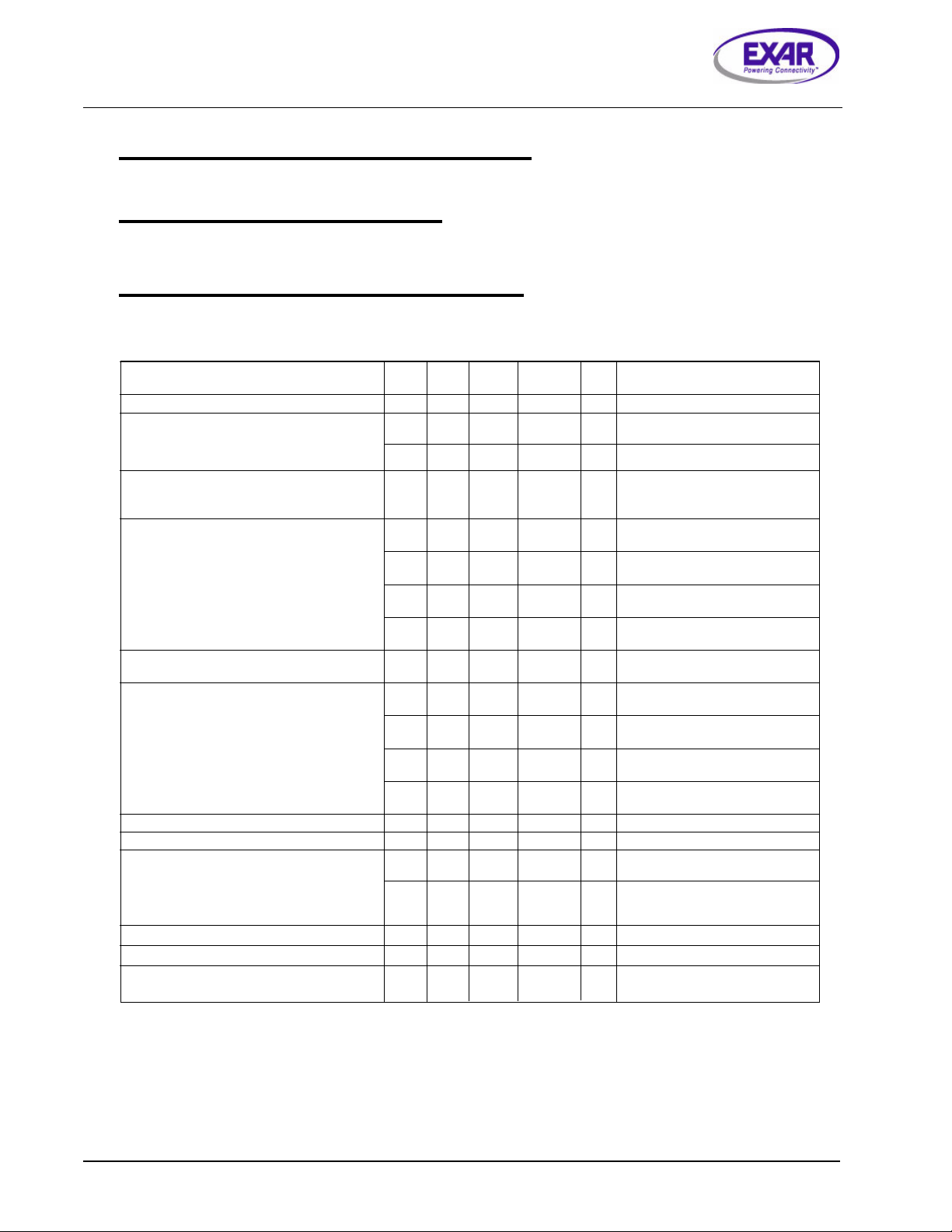
ABSOLUTE MAXIMUM RATINGS
Thermal Shutdown .................................................................... Internally Limited
Lead Temperature (Soldering, 5 seconds) ................................................. 260°C
Operating Junction Temperature Range .................................... -40°C to +125°C
RECOMMENDED OPERATING CONDITIONS
Input voltage ..................................................................................... +2.5V to 16V
Operating Junction Temperature Range .................................... -40°C to +125°C
Enable Input Voltage .............................................................................. 0V to V
SOT-23-5 (eJA) ................................................................................... See Note 1
TJ=25°C, VIN = V
apply over full temperature range -40°C to +85°C, unless otherwise specified.
+ 1V, IL = 100μA, CL = 1μF, and V
OUT
PARAMETER MIN TYP MAX UNITS CONDITIONS
Output Voltage Tolerance (V
) -1 +1 %V
OUT
-2 +2 z
Output Voltage Temperature Coefficient 57 ppm/°C z
Line Regulation 0.03 0.1 %/V
IN
ENABLE
0.2 z
Input Supply Voltage ......................................... -20V to +20V
Enable Input Voltage ......................................... -20V to +20V
ELECTRICAL CHARACTERISTICS
* 2.4V. The z denotes the specifications which
NOM
Load Regulation 0.1 0.2 %
0.5 z IL = 1mA to 150mA
z
Dropout Voltage (See Note 2) 30 50 mV IL = 100μA
(V
- VO) 70 z
IN
140 190 mV IL = 50mA
230 z
180 250 mV IL = 100mA
300 z
210 275 mV IL = 150mA
350 z
Quiescent Current (I
) 0.05 1 μA V
GND
5 z V
ENABLE
ENABLE
) 0.4V
) 0.25V
Ground Pin Current 70 125 μA IL = 100μA
) 150 z
(I
GND
350 600 IL = 50mA
800 z
750 1000 IL = 100mA
1500 z
1300 1900 IL = 150mA
2500 z
Ripple Rejection (PSRR) 70 dB
Current Limit (I
Output Noise (eNO) 300 μV
) 360 500 mA V
LIMIT
RMS
40 μV
RMS
= 0V
OUT
IL = 10mA, CL = 1μF, CIN= 1μF
(10Hz - 100kHz.)
IL = 10mA, CL = 10μF, C
1μF,C
=1μF,(10Hz - 100kHz)
IN
BYP
=
Input Voltage Level Logic Low (VIL) 0.4 V OFF
Input Voltage Level Logic High (VIL) 2.0 ON
ENABLE Input Current 0.01 2 μA VIL ) 0.4V
Note 1: The maximum allowable power dissipation is a function of maximum operating junction temperature, T
resistance, and the ambient, eJ
given: P
D (max)
regulator will go into thermal shutdown. The eJ
Note 2: Not applicable to output voltages of less than 2V.
= (T
3 20 V
, and the ambient temperature TA. The maximum allowable power dissipation at any ambient temperature is
A
- TA)/eJA, exceeding the maximum allowable power limit will result in excessive die temperature; thus, the
J (max)
of the SPX5205 is 220°C/W mounted on a PC board.
A
* 2.0V
IH
J (max)
2
, the junction to ambient thermal

SPX5205
REV. H 150mA, Low-Noise LDO Voltage Regulator
TYPICAL PERFORMANCE CHARACTERISTICS
1.40
1.20
1.00
0.80
(mA)
0.60
GND
I
0.40
0.20
0.00
3.3V Device
VIN= 3.2V
= 1.0μF
C
L
0 50 100 150
IL (mA)
Ground Current vs Load Current
110
100
90
80
(μA)
70
GND
I
60
50
40
30
4 6 8 10 12 14 16
Ground Current vs Input Voltage
VO = 3.3V
C
IL = 100μA
VIN (V)
= 1.0μF
L
2.00
3.3V Device
= 4.3V
V
IN
CL = 1.0μF
1.50
(mA)
1.00
GND
I
0.50
0.00
0 50 100 150
IL (mA)
Ground Current vs Load Current in Dropout
3.340
3.335
3.330
3.325
(V)
3.320
3.315
OUT
V
3.310
3.305
3.300
3.295
3.290
4 6 8 10 12 14 16
Output Voltage vs Input Voltage
3
VIN (V)
3.3V Device
CL= 1.0μF
I
= 100μA
L
 Loading...