

EXAR SP7651 Service Manual
®
1
2
3
4
5
6
7
8
9
10
11
12
13
14
15
16
17
18
19
20
21
22
23
24
25
26
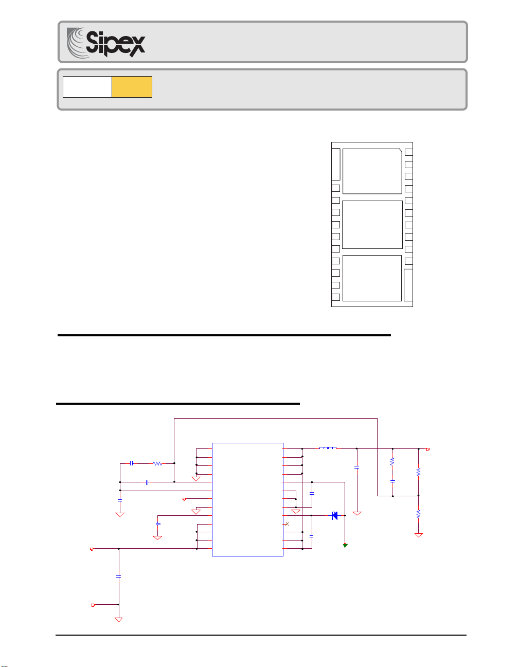
TOP VIEW
Heatsink Pad 1
Connect to Lx
Heatsink pad 2
Connect to GND
Heatsink pad 3
Connect to V
IN
P
GND
P
GND
GND
V
FB
COMP
UVIN
GND
SS
V
IN
LX
LX
LX
LX
V
CC
GND
GND
GND
BST
NC
LX
LX
LX
DFN PACKAGE
7mm x 4mm
SP7651
P
GND
V
IN
V
IN
V
IN
Blox
M
Preliminary
SP7651
Power
T
Blox
Wide Input Voltage Range 3A, 900kHz,
Buck Regulator
FEATURES
■ 2.5V to 20V Step Down Achieved Using Dual Input
■ Output Voltage down to 0.8V
■ 3A Output Capability (Up to 5A with Air Flow)
■ Built in Low R
Power FETs (40 mΩ typ)
DSON
■ Highly Integrated Design, Minimal Components
■ 900 kHz Fixed Frequency Operation
■ UVLO Detects Both V
CC
and V
IN
■ Over Temperature Protection
■ Short Circuit Protection with Auto-Restart
■ Wide BW Amp Allows Type II or III Compensation
■ Programmable Soft Start
■ Fast Transient Response
■ High Efficiency: Greater than 92% Possible
■ Asynchronous Start-Up into a Pre-Charged Output
■ Small 7mm x 4mm DFN Package
Now Available in Lead Free Packaging
DESCRIPTION
The SP7651 is a high voltage synchronous step-down switching regulator optimized for high efficiency. The part is
designed to be especially attractive for dual supply, 12V step down with 5V used to power the controller. This lower V
voltage minimizes power dissipation in the part. The SP7651 is designed to provide a fully integrated buck regulator
solution using a fixed 900kHz frequency, PWM voltage mode architecture. Protection features include UVLO, thermal
shutdown and output short circuit protection. The SP7651 is available in the space saving 7mm X 4mm DFN package.
TYPICAL APPLICATION CIRCUIT
CC
U1
PGND
PGND
PGND
GND
VFB
COMP
UVIN
GND
SS
VIN
VIN
VIN
VIN
SP7651
VCC
GND
GND
GND
26
LX
25
LX
24
LX
23
LX
22
21
20
19
18
BST
17
NC
16
LX
15
LX
14
LX
fs=900Khz
Notes:
1. U1 Bottom-Side Layout should
has three contacts isolated from
one another Vin SWNODE and GND
2. RSET=54.48/(Vout-0.8V) (KOhm)
1
1
RZ2
CZ2
15k,1%
VIN
12V
GND
Date: 2/18/05 SP7651 Wide Input Voltage Range 3A, 900kHz, Buck Regulator © Copyright 2005 Sipex Corporation
1,000pF
CP1
22pF
CF1
100pF
C1
22uF
16V
ENABLE
CSS
15nF
2
3
4
5
6
7
8
9
10
11
12
13
L1
4.7uH, Irate=3.87A
CVCC
2.2uF
DBST
SD101AWS
CBST
6800pF
+5V VCC
C3
22uF
6.3V
RZ3
7.15k,1%
CZ3
150pF
R1
68.1k,1%
RSET
21.5k,1%
(note 2)
VOUT
3.3V
0-3A
These are stress ratings only and functional operation of the device at
these ratings or any other above those indicated in the operation sections
of the specifications below is not implied. Exposure to absolute maximum
rating conditions for extended periods of time may affect reliability.
.................................................................................................. 7V
V
CC
...........................................................................................................................................
V
IN
...............................................................................................................................................
I
LX
BST ............................................................................................... 35V
BST-SWN ......................................................................... -0.3V to 7V
SWN ................................................................................... -1V to 20V
22V
5A
GH ......................................................................... -0.3V to BST+0.3V
GH-SWN ......................................................................................... 7V
All other pins .......................................................... -0.3V to V
Storage Temperature .................................................. -65°C to 150°C
Power Dissipation .................................................... Internally Limited
ESD Rating .......................................................................... 2kV HBM
Thermal Resistance ϑ
....................................................................................
JC
ELECTRICAL SPECIFICATIONS
ABSOLUTE MAXIMUM RATINGS
Unless otherwise specified: -40°C < T
LX = GND = 0V, UVIN = 3.0V, CV
The ♦ denotes the specifications which apply over the full temperature range, unless otherwise specified.
RETEMARAP.NIM.PYT.XAMSTINUSNOITIDNOC
TNERRUCTNECSEIUQ
< 85°C, -40°C< Tj <125°C, 4.5V < V
AMB
= 1µF, C
CC
= 0.1µF, CSS = 50nF, Typical measured at V
COMP
< 5.5V, 3V< Vin < 20V, BST=LX + 5V,
CC
CC
= 5V.
+0.3V
CC
5°C/W
V
CC
V
CC
)gnihctiwsoN(tnerruCylppuS5.13 AmVBFV9.0=
)gnihctiws(tnerruCylppuS821Am
♦
)gnihctiwsoN(tnerruCylppuSTSB2.04.0AmV
)gnihctiws(tnerruCylppuSTSB46Am
♦
V9.0=
BF
OLVU:NOITCETORP
V
CC
V
CC
dlohserhTtratSOLVU00.452.45.4V
siseretsyHOLVU001002003Vm
dlohserhTtratSNIVU3.25.256.2V
♦
siseretsyHNIVU002003004Vm
tnerruCtupnINIVU1AµV0.3=NIVU
ECNEREFERREIFILPMARORRE
ecnerefeRreifilpmArorrE297.0008.0808.0V
ecnerefeRreifilpmArorrE
erutarepmeTdnaeniLrevO
887.0008.0218.0V
♦
V
BFV;CC
erusaeM,.gifnoCniaGX2
Cº52=T,V5=
ecnatcudnocsnarTreifilpmArorrE6V/Am
niaGreifilpmArorrE06BddaoLoN
tnerruCkniSPMOC051AµV
tnerruCecruoSPMOC051AµV
V
BF
tnerruCsaiBtupnI05002AnVBFV8.0=
BF
BF
V9.0=PMOC,V9.0=
V2.2=PMOC,V7.0=
eloPlanretnI4zHM
pmalCPMOC5.2VV
BF
Cº52=AT,V7.0=
tneiciffeoC.pmeTpmalCPMOC2-Cº/Vm
Date: 2/18/05 SP7651 Wide Input Voltage Range 3A, 900kHz, Buck Regulator © Copyright 2005 Sipex Corporation
2
Unless otherwise specified: -40°C < T
GND = 0V, UVIN = 3.0V, CV
The ♦ denotes the specifications which apply over the full temperature range, unless otherwise specified.
= 1µF, C
CC
RETEMARAP.NIM.PYT.XAMSTINUSNOITIDNOC
edutilpmApmaR29.01.182.1V
< 85°C, -40°C<Tj<125°C, 4.5V < V
AMB
= 0.1µF, CSS = 50nF, Typical measured at V
COMP
< 5.5V, 3V<Vin<20V, BST=LX + 5V, LX =
CC
CC
= 5V.
HTAPYALEDPOOL&PMAR,ROTARAPMOCMWP:POOLLORTNOC
ELECTRICAL SPECIFICATIONS
T
tesffOPMAR1.1V
A
tneiciffeoC.pmeTtesffOPMAR2-Cº/Vm
htdiWesluPmuminiMHG09081sn
♦
oitaRytuDelballortnoCmumixaM2979%
oitaRytuDmumixaM001%selcyc02rofdilaV
oitaRrotallicsOlanretnI018009099zHk
♦
TRATSTFOS:SREMIT
:tnerruCegrahCSS01Aµ
:tnerruCegrahcsiDSS1Am
♦
lamrehT&tiucriCtrohS:NOITCETORP
egatloVdlohserhTtiucriCtrohS2.052.03.0V
♦
V
BF
tuoemiTpucciH002smVBFV5.0=
elcyCytuD%001ta
selcyCkcolCelbawollAforebmuN
selcyC02retfAesluPLGmuminiM5.0selcyCV
erutarepmeTnwodtuhSlamrehT541CºV
02selcyC
BF
BF
erutarepmeTyrevoceRlamrehT531Cº
PMOCPMAR,Cº52=
gnihctiwSstratsHGlitnu
oitaRytuDmumixaM
erofebtsujderusaeM
snigebgnislup
V2.0=SS,tneserPtluaF
VderusaeM
-)V8.0(
FER
V7.0=
V7.0=
siseretsyHlamrehT01Cº
EGATSREWOP:TUPTUO
V
RediShgiH
NOSD
RTEFsuonorhcnyS
NOSD
04 Ωm
04 Ωm
CC
T
V
CC
T
I;V5=
A3=
TUO
Cº52=
BMA
I;V5=
A3=
TUO
Cº52=
BMA
tnerruCtuptuOmumixaM3A
Date: 2/18/05 SP7651 Wide Input Voltage Range 3A, 900kHz, Buck Regulator © Copyright 2005 Sipex Corporation
3
#niPemaNniPnoitpircseD
3-1P
12-91,8,4DNG
5V
6PMOC
7NIVU
9SS
31-01V
62-32,61-41XLVdnanipsihtneewtebrotcudninatcennoC
22V
71CNtcennoCoN
DNG
BF
VU
NI
CC
PIN DESCRIPTION
reifitcersuonorhcnysehtrofnoitcennocdnuorG
erarevirdrewoprewoldnaCIehtfoyrtiucriclortnocehT.niPdnuorG
.tuoCfolanimret
VrevenehW.redividrotsiserlanretxenahguorht
BF
.edom
Vrodnuorgrehtiednanipsihtotdetcennoc
.pooledom
NI
ylppussaibV5lanretxeroftupnI
BF
VneewtebredividrotsiseratcennoC.egatlovniVroftupniOLVU
egatlovgnitarepomuminimtesot
.snoitidnoctluafllagnirudtnerruc)nim(Am1aaiv
.DNGPdnanipsihtneewtebroticapac
TUO
NI
)-(ehtotsecartdnuorgrehtomorfyletarapesnruteR.nipsihtotdecnerefer
tupnignitrevniehtsitI.nipnoitceteDtiucriCtrohSdnaegatloVkcabdeeF
roftniopkcabdeefegatlovtuptuoehtsasevresdnareifilpmArorrEehtfo
detsujdaebnacdnadesnessiegatlovtuptuoehT.retrevnoCkcuBeht
ehtwolebV52.0spord
puccihsretneCIehtdnadetcetedsitluaftiucrictrohsa,ecnereferevitisop
tupnignitrevniehtotdetcennocyllanretnisitI.reifilpmArorrEehtfotuptuO
dnanesohcsinoitanibmocretliflamitponA.rotarapmocMWPehtfo
egatlovehtezilibatsot
dna
ehttesotDNGdnaSSneewtebroticapaclanretxenatcennoC.tratStfoS
woldlehsinipSSehT.tnerrucecruosAµ01ehtnodesabetartratstfos
gnilpuocedaecalP.TEFSOMlennahc-NedishgihehtotnoitcennoctupnI
THEORY OF OPERATION
General Overview
The SP7651 is a fixed frequency, voltage mode,
synchronous PWM regulator optimized for high
efficiency. The part has been designed to be
especially attractive for split plane applications
utilizing 5V to power the controller and 2.5V to
28V for step down conversion.
The SP7651 contains two unique control features that are very powerful in distributed applications. First, asynchronous driver control is
enabled during start up, to prohibit the low side
NFET from pulling down the output until the
high side NFET has attempted to turn on. Second, a 100% duty cycle timeout ensures that the
The heart of the SP7651 is a wide bandwidth
transconductance amplifier designed to accommodate Type II and Type III compensation
schemes. A precision 0.8V reference, present on
low side NFET is periodically enhanced during
extended periods at 100% duty cycle. This guarantees the synchronized refreshing of the BST
capacitor during very large duty ratios.
the positive terminal of the error amplifier permits the programming of the output voltage
down to 0.8V via the VFB pin. The output of the
error amplifier, COMP, which is compared to a
1.1V peak-to-peak ramp is responsible for trailing edge PWM control. This voltage ramp, and
PWM control logic are governed by the internal
oscillator that accurately sets the PWM fre-
The SP7651 also contains a number of valuable
protection features. Programmable UVLO allows the user to set the exact V
value at which
IN
the conversion voltage can safely begin down
conversion, and an internal VCC UVLO ensures
that the controller itself has enough voltage to
properly operate. Other protection features in-
quency to 900kHz.
Date: 2/18/05 SP7651 Wide Input Voltage Range 3A, 900kHz, Buck Regulator © Copyright 2005 Sipex Corporation
4
 Loading...