

Exar SP483CN-L, SP483EN-L, SP485CN-L, SP485CS-L, SP485EN-L Schematic [ru]
...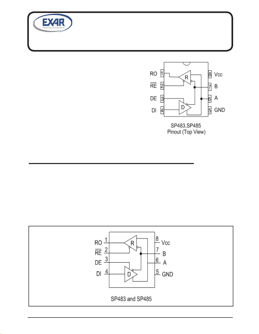
SP483 / SP485
Low Power Half-Duplex RS-485 Transceivers
FEATURES
• +5V Only
• Low Power BiCMOS
• Driver / Receiver Enable
• Slew Rate Limited Driver for Low EMI (SP483)
• Low Power Shutdown mode (SP483)
• RS-485 and RS-422 Drivers/Receivers
DESCRIPTION
The SP483 and SP485 are a family of half-duplex transceivers that meet the specications
of RS-485 and RS-422. Their BiCMOS design allows low power operation without sacricing
performance. The SP485 meets the requirements of RS-485 and RS-422 up to 5Mbps. Additionally, the SP483 is equipped with a low power Shutdown mode. The SP483 is internally
slew rate limited to reduce EMI and can meet the requirements of RS-485 and RS-422 up
to 250kbps.
Exar Corporation 48720 Kato Road, Fremont CA, 94538 • 510-668-7017 • www.exar.com SP483_SP485_101_062711
1
ABSOLUTE MAXIMUM RATINGS
These are stress ratings only and functional operation
of the device at these ratings or any other above those
indicated in the operation sections of the specications
below is not implied. Exposure to absolute maximum
rating conditions for extended periods of time may
affect reliability.
VCC.......................................................................+7V
Input Voltages
Logic.........................-0.3V to (Vcc + 0.5V)
Drivers......................-0.3V to (Vcc + 0.5V)
Receivers.........................................+/-15V
Output Voltages
Logic.........................-0.3V to (Vcc + 0.5V)
Drivers.............................................+/-15V
Receivers..................-0.3V to (Vcc + 0.5V)
Storage Temperature.......................-65˚C to +150˚C
Power Dissipation
8-pin NSOIC...................................................500mW
T
to T
and VCC = 5V +/-5% unless otherwise noted.
MIN
MAX
ELECTRICAL CHARACTERISTICS
PARAMETERS MIN. TYP. MAX. UNITS CONDITIONS
SP483/SP485 DRIVER
DC Characteristics
Differential Output Voltage Vcc Volts Unloaded; R = ∞ ; see gure 1
Differential Output Voltage 2 Vcc Volts With Load; R = 50Ω (RS-422);
see figure 1
Differential Output Voltage 1.5 Vcc Volts With Load; R = 27Ω (RS-485);
see figure 1
Change in Magnitude of Driver
0.2 Volts R = 27Ω or R = 50Ω; see figure 1
Differential Output Voltage for
Complimentary states
Driver Common Mode Output
3 Volts R = 27Ω or R = 50Ω; see figure 1
Voltage
Input High Voltage 2.0 Volts Applies to DE, DI, RE
Input Low Voltage 0.8 Volts Applies to DE, DI, RE
Input Current +/-10 µA Applies to DE, DI, RE
Driver Short Circuit Current,
V
= HIGH
OUT
Driver Short Circuit Current,
V
= LOW
OUT
250 mA -7V ≤ VO ≤ +12V
250 mA -7V ≤ VO ≤ +12V
SP485 DRIVER
AC Characteristics
Maximum Data Rate 5 Mbps RE = 5V, DE = 5V
Driver Input to Output, t
Driver Input to Output, t
PLH
PHL
30 60 ns Figures 3 and 5, R
CL1 = CL2 = 100pF
30 60 ns Figures 3 and 5, R
CL1 = CL2 = 100pF
= 54Ω,
DIFF
= 54Ω,
DIFF
Driver Skew 5 10 ns Figures 3 and 5,
t
= |t
- t
SKEW
DPHL
Driver Rise or Fall Time 15 40 ns From 10%-90%; R
CL1 = CL2 = 100pF; see gures 3
DPLH
|
DIFF
= 54Ω
and 5
Exar Corporation 48720 Kato Road, Fremont CA, 94538 • 510-668-7017 • www.exar.com SP483_485_101_062711
2
T
to T
and VCC = 5V +/-5% unless otherwise noted.
MIN
MAX
ELECTRICAL CHARACTERISTICS
PARAMETERS MIN. TYP. MAX. UNITS CONDITIONS
SP485 DRIVER (continued)
AC Characteristics
Driver Enable to Output High 40 70 ns CL = 100pF, see gures 4 and 6,
S2 closed
Driver Enable to Output Low 40 70 ns CL = 100pF, see gures 4 and 6,
S1 closed
Driver Disable Time from High 40 70 ns CL = 15pF, see gures 2 and 8,
S2 closed
Driver Disable Time from Low 40 70 ns CL = 15pF, see gures 2 and 8,
S1 closed
SP483/SP485 RECEIVER
DC Characteristics
Differential Input Threshold -0.2 +0.2 Volts -7V ≤ VCM ≤ +12V
Input Hysteresis 10 mV VCM = 0V
Output Voltage High 2.4 5 Volts IO = -4mA, VID = +200mV
Output Voltage Low 0.0 0.4 Volts IO = +4mA, VID = -200mV
Three-State ( High Impedance)
+/-1 µA 0.4V ≤ VO ≤ 2.4V; RE = 5V
Output Current
Input Resistance 12 15 kΩ -7V ≤ VCM ≤ +12V
Input Current (A, B); VIN = 12V +1.0 mA DE = 0V, VCC = 0V or 5.25V,
VIN = 12V
Input Current (A, B); VIN = -7V -0.8 mA DE = 0V, VCC = 0V or 5.25V,
VIN = -7V
Short-Circuit Current 95 mA 0V ≤ VCM ≤ V
CC
SP485 RECEIVER
AC Characteristics
Maximum Data Rate 5 Mbps RE = 0V, DE = 0V
Receiver Input to Output 20 45 200 ns t
Receiver Input to Output 20 45 200 ns t
Differential Receiver Skew
|t
- t
|
PHL
PLH
13 ns R
Figures 3 and 7,
PLH ;
R
= 54Ω, CL1 = CL2 = 100pF
DIFF
Figures 3 and 7,
PHL ;
R
= 54Ω, CL1 = CL2 = 100pF
DIFF
= 54Ω, CL1 = CL2 = 100pF,
DIFF
Figures 3 and 7
Receiver Enable to Output Low 45 70 ns CRL = 15pF, Figures 2 and 8;
S1 Closed
Receiver Enable to Output High 45 70 ns CRL = 15pF, Figures 2 and 8;
S2 Closed
Receiver Disable from LOW 45 70 ns CRL = 15pF, Figures 2 and 8;
S1 Closed
Receiver Disable from High 45 70 ns CRL = 15pF, Figures 2 and 8;
S2 Closed
Exar Corporation 48720 Kato Road, Fremont CA, 94538 • 510-668-7017 • www.exar.com SP483_SP485_101_062711
3
T
to T
and VCC = 5V +/-5% unless otherwise noted.
MIN
MAX
ELECTRICAL CHARACTERISTICS
PARAMETERS MIN. TYP. MAX. UNITS CONDITIONS
POWER REQUIREMENTS
Supply Voltage V
CC
+4.75 +5.25 Volts
Supply Current
SP485 900 µA No Load; RE, DI = 0V or VCC;
DE = V
CC
900 µA No Load; RE = 0V, DI = 0V or 5V;
DE = 0V
SP483 600 µA No Load; RE, DI = 0V or VCC;
DE = V
CC
600 µA No Load; RE = 0V, DI = 0V or 5V;
DE = 0V
SP483 10 µA Shutdown Mode; DE = 0V, RE = V
ENVIRONMENTAL AND MECHANICAL
Operating Temperature
Commercial (_C_) 0 70 ºC
Industrial (_E_) -40 +85 ºC
Storage Temperature -65 +150 ºC
Package: Plastic DIP (_P), NSOIC (_N)
CC
Exar Corporation 48720 Kato Road, Fremont CA, 94538 • 510-668-7017 • www.exar.com SP483_485_101_062711
4
 Loading...