

Page 1
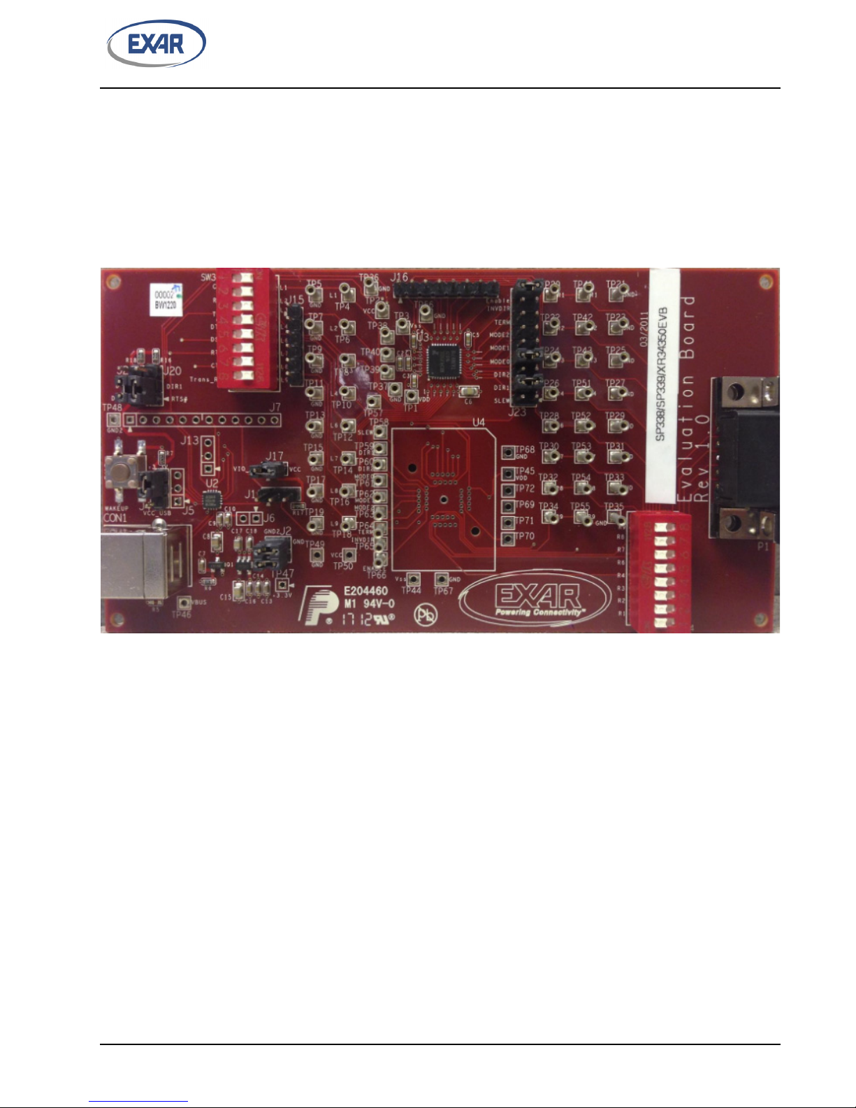
REV. 2.0.1 SP338/SP339/XR34350 EVALUATION BOARD USER’S MANUAL
Evaluation Board User’s Manual
SP338/SP339/XR34350EVB
1
Page 2

XR21B1411
SP338
SP339
XR34350
SW3 SW4
USB
Connector
DB9
Connector
SP338/SP339/XR34350 EVALUATION BOARD USER’S MANUAL REV. 2.0.1
1.0 INTRODUCTION
This user’s manual is for the SP338/SP339/XR34350 evaluation board. The SP338, SP339 and XR34350 are
pin compatible devices and are all offered in the 40-pin QFN package. The primary difference is that the SP339
and XR34350 only have 4 modes of operation (2 mode control pins) while the SP338 has 8 modes of operation
(3 mode control pins). Table 1 shows the different devices and packages that this evaluation board supports,
and the corresponding ordering part numbers for each.
ABLE 1: PACKAGE LIST
T
DEVICE
RDERING PART NUMBER
O
XR34350IL XR34350ILEVB 40-pin QFN U3
SP338EER1-L SP338EER1-0A-EB 40-pin QFN U3
SP339EER1-L SP339EER1-0A-EB 40-pin QFN U3
EVALUATION BOARD
ORDERING PART NUMBER
2.0 EVALUATION BOARD OVERVIEW
A block diagram of the evaluation board is shown in
F
IGURE 1. EVALUATION BOARD BLOCK DIAGRAM
PACKAGE
Figure 1 below..
DEVICE
DEVICE
LOCATION
In addition to the DUT (SP338/SP339/XR34350), there is an Exar XR21B1411 1-ch USB UART on this
evaluation board. When shipped from the factory, the SW3 and SW4 switches are off. Therefore, the SP338/
339/XR34350 is isolated from both the XR21B1411 and the DB9 connector. To enable the connections
between the XR21B1411 and the SP338/339/XR34350, place all switches on SW3 in the ON position. To
enable the connections between the SP338/339/XR34350 and the DB9 connector, place all switches on SW4
to the ON position. All SP338/339/XR34350 signals are accessible from the test points on the board. The test
points are shown in each figure showing the modes.
2.1 Mode Selection
The modes of the SP338 are selected
? Pins 7 & 8 - labeled MODE0 on the board
? Pins 9 & 10 - labeled MODE1 on the board
? Pins 11 & 12 - labeled MODE2 on the board
Note that the SP339 does not have a MODE2 pin, so the SP3
MODE0 pins.
using the following pins at J23:
39 modes are only controlled via the MODE1 and
2
Page 3
TP4
TP6
TP8
TP10
TP12
TP14
TP16
TP18
Mode0 = 0
Mode1 = 0
Mode2 = 0
Enable = 1
Vcc
L1
L2
L3
L4
L6
L7
L8
L9
Vcc
11 12 13 14 15 16 17 18 19 20
40 39 38 37 36 35 34 33 32 31
1
2
3
4
5
6
7
8
9
10
30
29
28
27
26
25
24
23
22
21
All pull-downs 330kO
V+
C2+
Vcc
C1+
C1-
C2-
V-
Vcc
C3
0.1µF
C2
0.1µF
C1
0.1µF
C4
0.1µF
Cc
1.0µF
R3
R4
T3
R5
T2
T1
R2
R1
REV. 2.0.1 SP338/SP339/XR34350 EVALUATION BOARD USER’S MANUAL
The SP338/339/XR34350 have internal pull-down resistors on these pins. So the corresponding MODE pins
will be ’0’ unless a jumper is installed on the J23 pins listed above to change the MODE bit to ’1’.
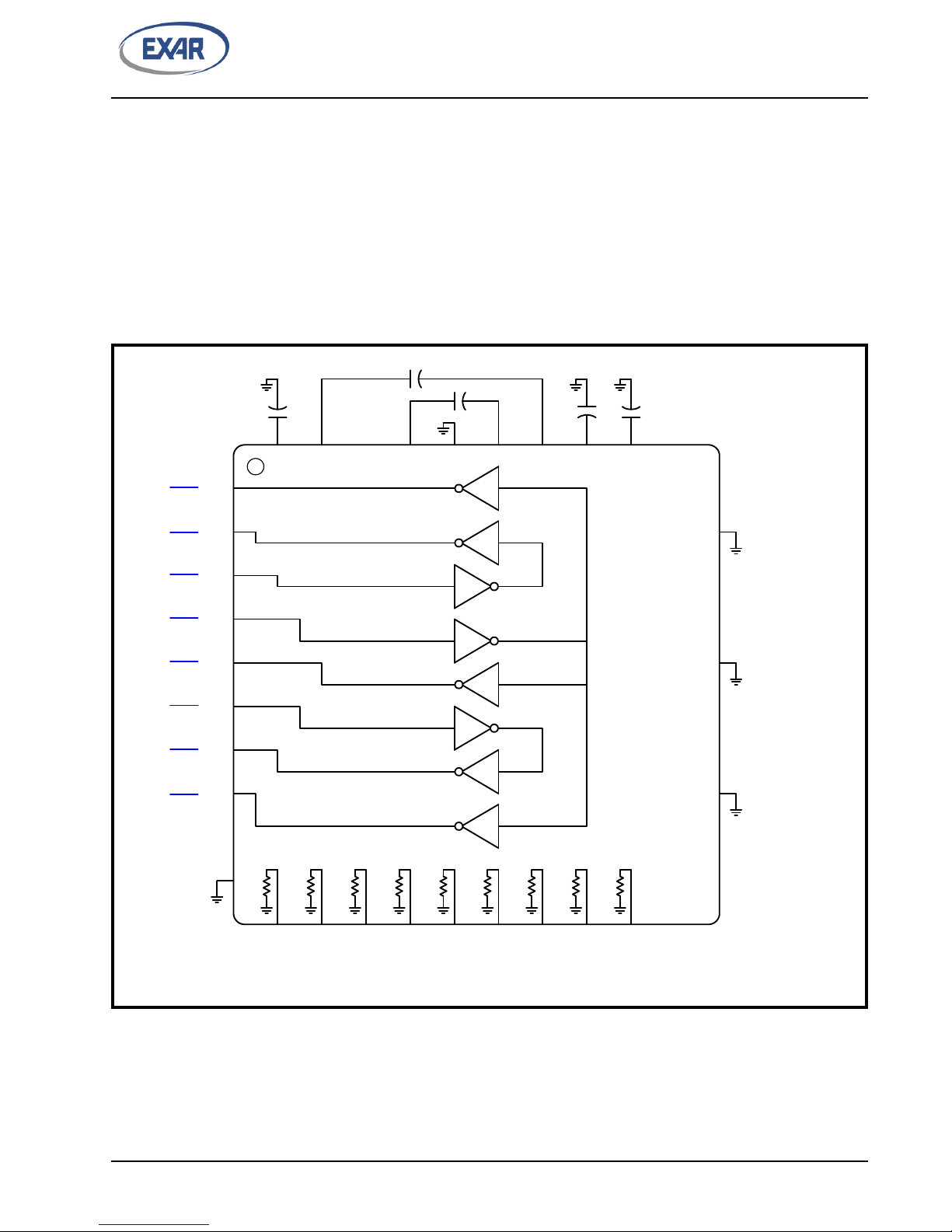
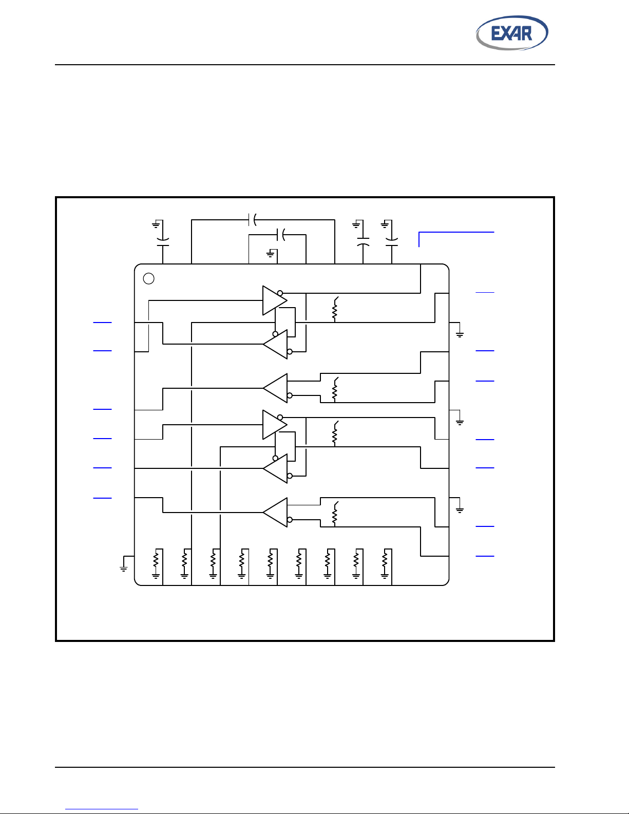
2.1.1 Loopback Mode
Figure 2 below shows the SP338/339/XR34350 configured in the Loopback mode.
? J23 Pins 7 & 8 (MODE0) - ’0’
? J23 Pins 9 & 10 (MODE1) - ’0’
? J23 Pins 11 & 12 (MODE2) - ’0’
This mode can be used for diagnostic purposes.
F
IGURE 2. LOOPBACK MODE
3
Page 4
L1
L2
L3
L4
L6
L7
L8
L9
Vcc
R2
R3
R4
R6
R7
R8
R9
11 12 13 14 15 16 17 18 19 20
40 39 38 37 36 35 34 33 32 31
1
2
3
4
5
6
7
8
9
10
30
29
28
27
26
25
24
23
22
21
All pull-downs 330kO
R1
V+
C2+
Vcc
C1+
C1-
C2-
V-
Vcc
C3
0.1µF
C2
0.1µF
C1
0.1µF
C4
0.1µF
Cc
1.0µF
R3
R4
T3
R5
T2
T1
R2
R1
5kO
5kO
5kO
5kO
5kO
TP4
TP6
TP8
TP10
TP12
TP14
TP16
TP18
TP34, TP55
TP32, TP54
TP30, TP53
TP28, TP52
TP26, TP51
TP24, TP43
TP22, TP42
TP20, TP41
Slew
Mode0 = 1
Mode1 = 0
Mode2 = 0
Enable = 1
Vcc
11 12 13 14 15 16 17 18 19 20
SP338/SP339/XR34350 EVALUATION BOARD USER’S MANUAL REV. 2.0.1
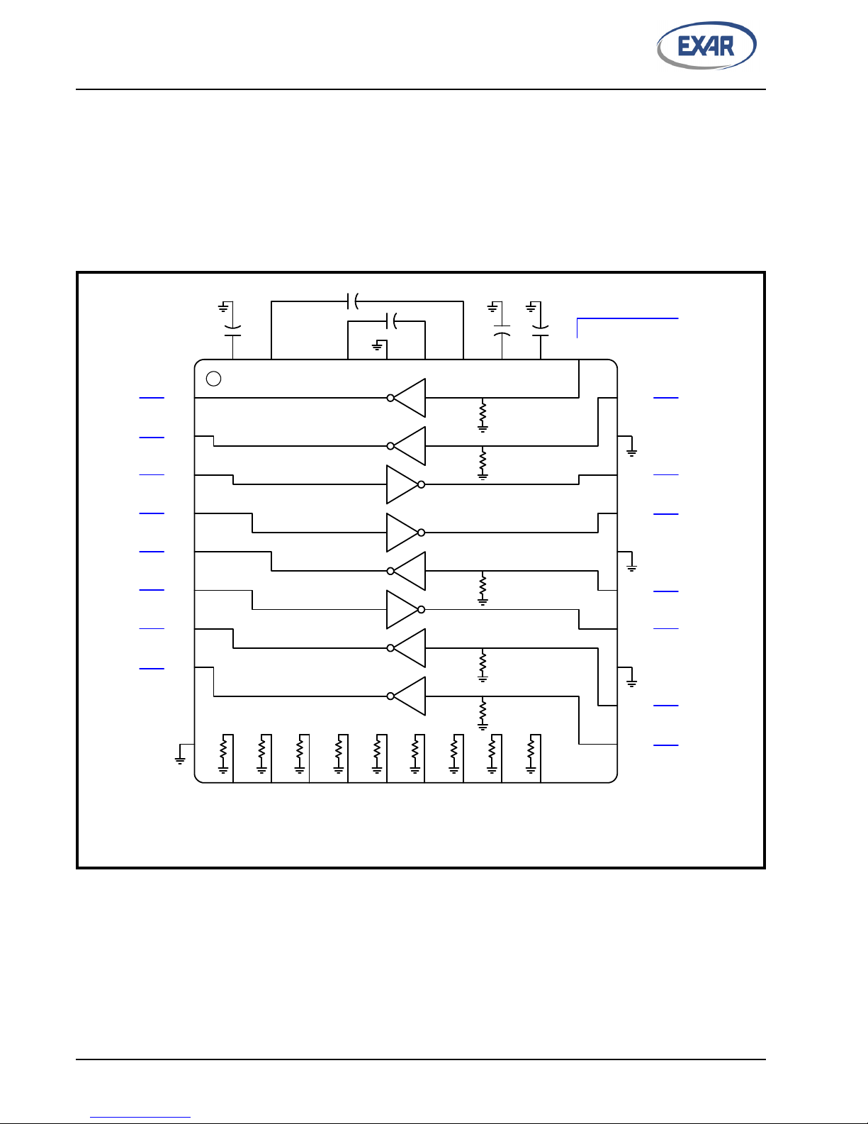
2.1.2 RS-232 Mode
Figure 3 below shows the SP338/339/XR34350 configured in the RS-232 mode.
? J23 Pins 7 & 8 (MODE0) - ’1’ (jumper installed between these pins)
? J23 Pins 9 & 10 (MODE1) - ’0’
? J23 Pins 11 & 12 (MODE2) - ’0’
This is the default setting on the evaluation
F
IGURE 3. RS-232 MODE
board when shipped from the factory.
4
Page 5
TP6
TP8
TP22, TP42
TP20, TP41
Slew
Dir1
Mode0 = 0
Mode1 = 1
Mode2 = 0
Term
InvDir
Enable = 1
Vcc
L1 = 1
L2
L3
L6 = 1
L8 = 1
L9 = 1
Vcc
R1
T1
R2
120O
11 12 13 14 15 16 17 18 19 20
40 39 38 37 36 35 34 33 32 31
1
2
3
4
5
6
7
8
9
10
30
29
28
27
26
25
24
23
22
21
All pull-downs 330kO
R1
V+
C2+
Vcc
C1+
C1-
C2-
V-
Vcc
C3
0.1µF
C2
0.1µF
C1
0.1µF
C4
0.1µF
Cc
1.0µF
REV. 2.0.1 SP338/SP339/XR34350 EVALUATION BOARD USER’S MANUAL
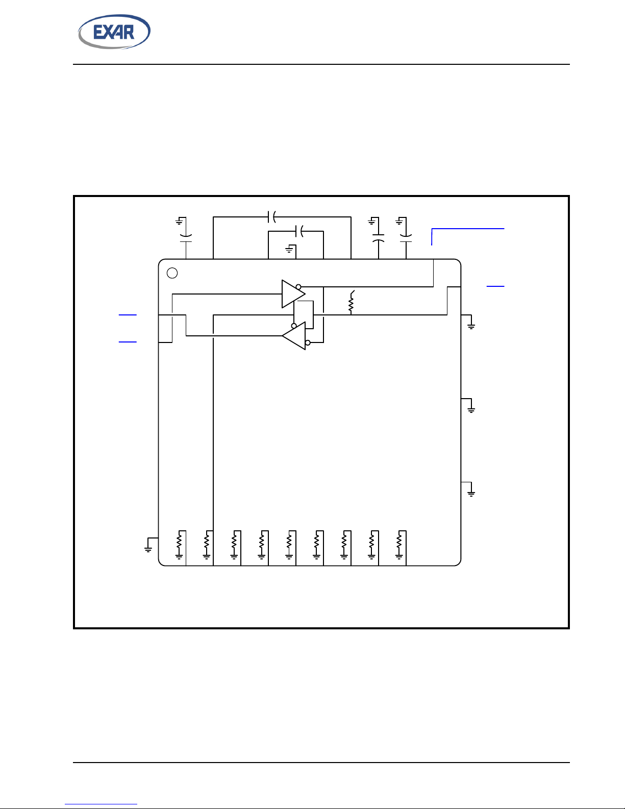
2.1.3 Half-Duplex RS-485 Mode #1
Figure 4 below shows the SP338/339/XR34350 configured in the half-duplex RS-485 mode #1.
? J23 Pins 7 & 8 (MODE0) - ’0’
? J23 Pins 9 & 10 (MODE1) - ’1’ (jumper installed between these pins)
? J23 Pins 11 & 12 (MODE2) - ’0’
The RS-485 signals are also accessible at J16.
F
IGURE 4. HALF-DUPLEX RS-485 MODE #1
5
Page 6
Slew
Dir1
Mode0 = 1
Mode1 = 1
Mode2 = 0
Term
InvDir
Enable = 1
Vcc
T1
R1
R2
R3
R4
11 12 13 14 15 16 17 18 19 20
40 39 38 37 36 35 34 33 32 31
1
2
3
4
5
6
7
8
9
10
30
29
28
27
26
25
24
23
22
21
120O
All pull-downs 330kO
R1
V+
C2+
Vcc
C1+
C1-
C2-
V-
Vcc
C3
0.1µF
C2
0.1µF
C1
0.1µF
C4
0.1µF
Cc
1.0µF
L1 = 1
L2
L3
L6 = 1
L8 = 1
L9 = 1
Vcc
TP6
TP8
TP26, TP51
TP24, TP43
TP22, TP42
TP20, TP41
SP338/SP339/XR34350 EVALUATION BOARD USER’S MANUAL REV. 2.0.1
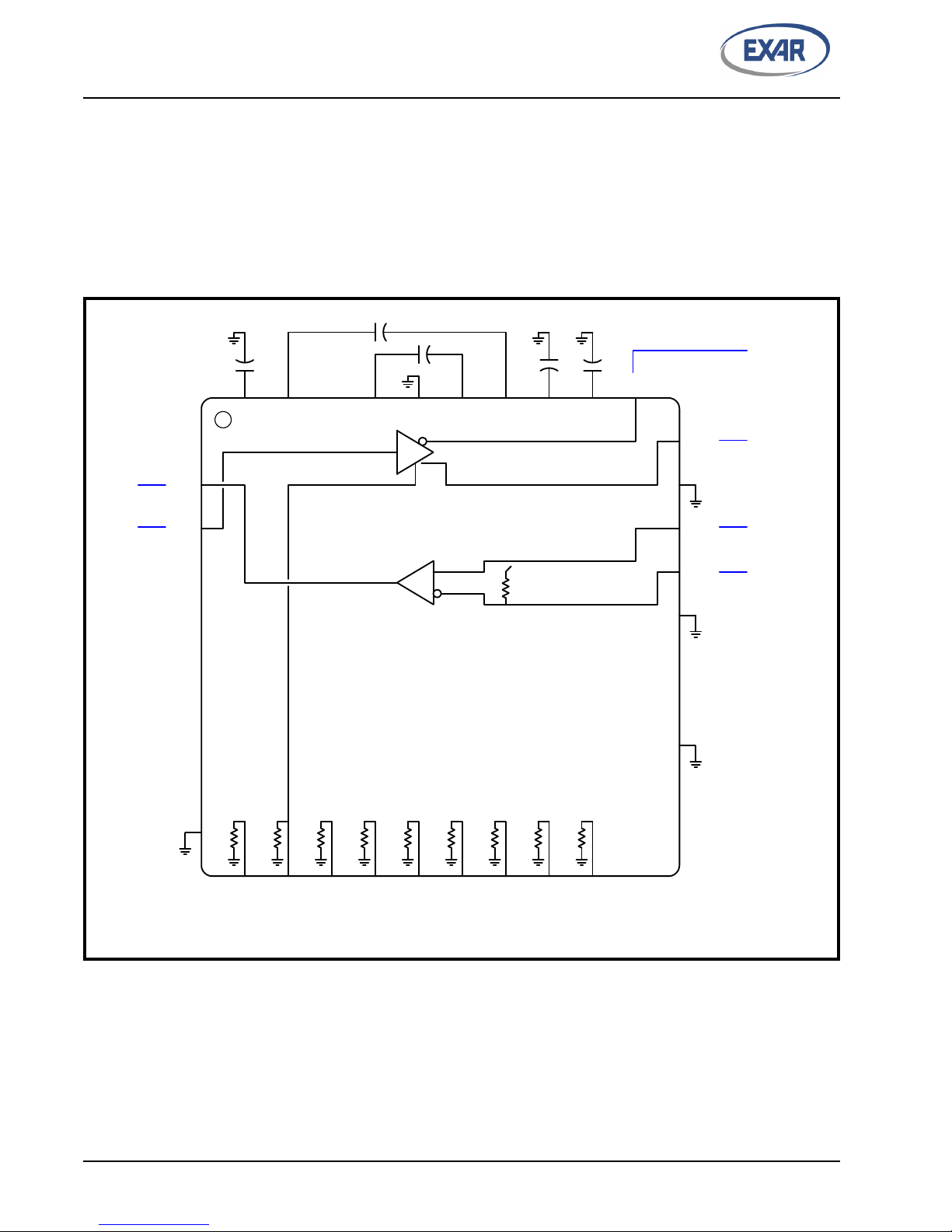
2.1.4 Full-Duplex RS-485/422 Mode #1
Figure 5 below shows the SP338/339/XR34350 configured in the full-duplex RS-485/422 mode #1.
? J23 Pins 7 & 8 (MODE0) - ’1’ (jumper installed between these pins)
? J23 Pins 9 & 10 (MODE1) - ’1’ (jumper installed between these pins)
? J23 Pins 11 & 12 (MODE2) - ’0’
The RS-485 signals are also accessible at J16.
F
IGURE 5. FULL-DUPLEX RS-485 MODE #1
6
Page 7
TP6
TP8
TP26, TP51
TP24, TP43
TP22, TP42
TP20, TP41
Slew
Dir1
Dir2
Mode0 = 0
Mode1 = 0
Mode2 = 1
Term
InvDir
Enable = 1
Vcc
T1
R1
T2
R2
R2
R3
R4
R6
R7
R8
R9
11 12 13 14 15 16 17 18 19 20
40 39 38 37 36 35 34 33 32 31
1
2
3
4
5
6
7
8
9
10
30
29
28
27
26
25
24
23
22
21
120O
120O
All pull-downs 330kO
R1
V+
C2+
Vcc
C1+
C1-
C2-
V-
Vcc
C3
0.1µF
C2
0.1µF
C1
0.1µF
C4
0.1µF
Cc
1.0µF
L1 = 1
L2
L3
L6 = 1
L7
L8
L9 = 1
Vcc
TP10
TP12
TP14
TP16
TP18
TP34, TP55
TP32, TP54
TP30, TP53
TP28, TP52
REV. 2.0.1 SP338/SP339/XR34350 EVALUATION BOARD USER’S MANUAL
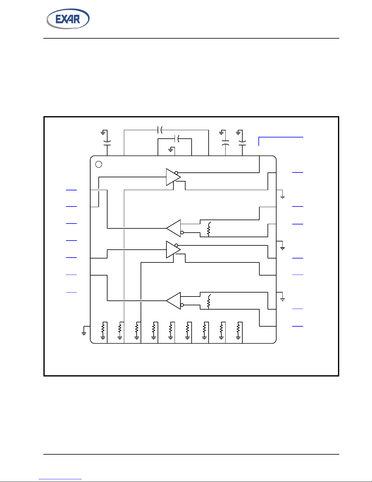
2.1.5 Full-Duplex RS-485/422 Mode #2 (SP338 only)
Figure 6 below shows the SP338 configured in the full-duplex RS-485/422 mode #2.
? J23 Pins 7 & 8 (MODE0) - ’0’
? J23 Pins 9 & 10 (MODE1) - ’0’
? J23 Pins 11 & 12 (MODE2) - ’1’ (jumper installed between these pins)
The RS-485 signals are also accessible at J16.
F
IGURE 6. FULL-DUPLEX RS-485 MODE #2
7
Page 8
TP6
TP8
TP26, TP51
TP20, TP41
TP34, TP55
TP30, TP53
Slew
Dir1
Mode0 = 1
Mode1 = 0
Mode2 = 1
Term
InvDir
Enable = 1
Vcc
T1
R1
R4
R7
R9
11 12 13 14 15 16 17 18 19 20
40 39 38 37 36 35 34 33 32 31
1
2
3
4
5
6
7
8
9
10
30
29
28
27
26
25
24
23
22
21
120O
All pull-downs 330kO
R1
V+
C2+
Vcc
C1+
C1-
C2-
V-
Vcc
C3
0.1µF
C2
0.1µF
C1
0.1µF
C4
0.1µF
Cc
1.0µF
L1 = 1
L2
L3
L6 = 1
L8 = 1
L9 = 1
Vcc
SP338/SP339/XR34350 EVALUATION BOARD USER’S MANUAL REV. 2.0.1
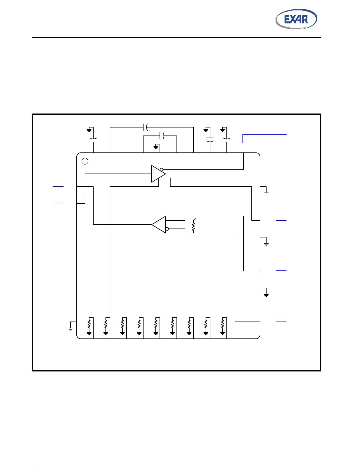
2.1.6 Full-Duplex RS-485/422 Mode #3 (SP338 Only)
Figure 7 below shows the SP338 configured in the full-duplex RS-485/422 mode #3.
? J23 Pins 7 & 8 (MODE0) - ’1’ (jumper installed between these pins)
? J23 Pins 9 & 10 (MODE1) - ’0’ (jumper installed between these pins)
? J23 Pins 11 & 12 (MODE2) - ’1’ (jumper installed between these pins)
The RS-485 signals are also accessible at J16.
F
IGURE 7. FULL-DUPLEX RS-485 MODE #3
8
Page 9
R2
R3
R4
R6
R7
R8
R9
TP6
TP8
TP26, TP51
TP22, TP42
TP20, TP41
Slew
Dir1
Mode0 = 0
Mode1 = 1
Mode2 = 1
Term
InvDir
Enable = 1
Vcc
R1
T1
R4
120O
11 12 13 14 15 16 17 18 19 20
40 39 38 37 36 35 34 33 32 31
1
2
3
4
5
6
7
8
9
10
30
29
28
27
26
25
24
23
22
21
All pull-downs 330kO
R1
V+
C2+
Vcc
C1+
C1-
C2-
V-
Vcc
C3
0.1µF
C2
0.1µF
C1
0.1µF
C4
0.1µF
Cc
1.0µF
L1 = 1
L2
L3
L6 = 1
L8 = 1
L9 = 1
Vcc
REV. 2.0.1 SP338/SP339/XR34350 EVALUATION BOARD USER’S MANUAL
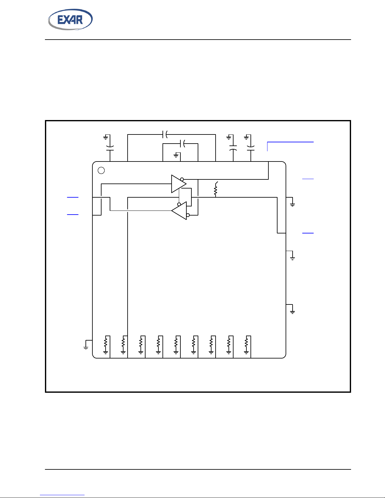
2.1.7 Half-Duplex RS-485 Mode #2 (SP338 Only)
Figure 8 below shows the SP338/339/XR34350 configured in the half-duplex RS-485/422 mode #2.
? J23 Pins 7 & 8 (MODE0) - ’0’
? J23 Pins 9 & 10 (MODE1) - ’1’ (jumper installed between these pins)
? J23 Pins 11 & 12 (MODE2) - ’1’ (jumper installed between these pins)
The RS-485 signals are also accessible at J16.
F
IGURE 8. HALF-DUPLEX RS-485 MODE #2
9
Page 10
R2
R3
R4
R6
R7
R8
R9
TP6
TP8
TP12
TP14
TP16
TP18
TP34, TP55
TP32, TP54
TP30, TP53
TP28, TP52
TP26, TP51
TP24, TP43
TP22, TP42
TP20, TP41
Slew
Dir1
Dir2
Mode0 = 1
Mode1 = 1
Mode2 = 1
Term
InvDir
Enable = 1
Vcc
L1 = 1
L2
L3
L6
L7
L8
L9
Vcc
R1
T1
R2
R3
T2
R4
R2
R3
R4
R6
R7
R8
R9
120O
11 12 13 14 15 16 17 18 19 20
40 39 38 37 36 35 34 33 32 31
1
2
3
4
5
6
7
8
9
10
30
29
28
27
26
25
24
23
22
21
120O
120O
120O
All pull-downs 330kO
R1
V+
C2+
Vcc
C1+
C1-
C2-
V-
Vcc
C3
0.1µF
C2
0.1µF
C1
0.1µF
C4
0.1µF
Cc
1.0µF
SP338/SP339/XR34350 EVALUATION BOARD USER’S MANUAL REV. 2.0.1
2.1.8 RS-485/422 Mixed Duplex Mode (SP338 Only)
Figure 9 below shows the SP338 configured in the full-duplex RS-485/422 mode.
? J23 Pins 7 & 8 (MODE0) - ’1’ (jumper installed between these pins)
? J23 Pins 9 & 10 (MODE1) - ’1’ (jumper installed between these pins)
? J23 Pins 11 & 12 (MODE2) - ’1’ (jumper installed between these pins)
The RS-485 signals are also accessible at J16.
F
IGURE 9. RS-485/422 MIXED DUPLEX MODE
10
Page 11

REV. 2.0.1 SP338/SP339/XR34350 EVALUATION BOARD USER’S MANUAL
2.2 Additional Control Signals
2.2.1 SLEW
By default, slew rate limiting is disabled. To enable slew rate limiting, place a jumper between J23 pins 1 & 2.
2.2.2 DIR1
This pin is only applicable in the half-duplex and full-duplex RS-485/RS-422 modes. The DIR1 signal can
manually be controlled at J23 pins 3 & 4. There’s an internal pull-down resistor on this pin. To change the logic
level on this pin, install a jumper at J23 pins 3 & 4.
2.2.2.1 Full-Duplex Mode
In the full-duplex modes, this pin enables/disables the T1 differential driver. A logic low disables the T1
differential driver. A logic high enables the T1 differential driver.
2.2.2.2 Half-Duplex Mode
In the half-duplex modes, this pin controls the direction of the T1 different driver or R1 differential receiver. A
logic low enables the R1 differential receiver and disables the T1 differential driver. A logic high enables the T1
differential driver and disablesthe R1 differential receiver.
2.2.3 DIR2
This pin is only applicable in the half-duplex and full-duplex RS-485/RS-422 modes. The DIR2 signal can
manually be controlled at J23 pins 5 & 6. There is an internal pull-down resistor on this pin. To change the
logic level on this pin, install a jumper at J23 pins 5 & 6.
2.2.3.1 Full-Duplex Mode
In the full-duplex modes, this pin enables/disables the T2 differential driver. A logic low disables the T2
differential driver. A logic high enables the T2 differential driver.
2.2.3.2 Half-Duplex Mode
In the half-duplex modes, this pin controls the direction of the T2 different driver or R1 differential receiver. A
logic low enables the R2 differential receiver and disables the T2 differential driver. A logic high enables the T2
differential driver and disablesthe R2 differential receiver.
2.2.4 TERM
This pin is only applicable in the half-duplex and full-duplex RS-485/RS-422 modes. The TERM pin enables/
disables the internal termination resistor. There is an in internal pull-down resistor on this pin so the internal
termination resistor is disabled when there’s no jumper across J23 pins 13 & 14. Install a jumper across J23
pins 13 & 14 to enable the internal termination resistor.
2.2.5 INVDIR
This pin is only applicable int he half-duplex and full-duplex RS-485/RS-422 modes. The INVDIR inverts the
polarity of the DIR1 and DIR2 pins. This pin has an internal pull-down resistor. The polarity inversion can be
enabled by installing a jumper across J23 pins 15 & 16.
2.2.6 ENABLE
This pin enables/disables the SP338/339/XR34350. This pin has an internal pull-down. When shipped from
the factory, there will be a jumper installed across J23 pins 17 & 18 to enable the SP338/339/XR34350.
11
Page 12

SP338/SP339/XR34350 EVALUATION BOARD USER’S MANUAL REV. 2.0.1
3.0 EVALUATING THE SP338/339/XR34350 TRANSCEIVER ONLY
When evaluating just the SP338/339/XR34350, an external power supply can be used or power from a USB
port can be used.
3.1 External Power Supply
An external +3.3V or +5V power supply can be applied at TP2. The USB cable should not be plugged into a
USB port and J17 should not be installed. Of course, there should be a common ground between the external
power supply and the SP338/339/XR34350.
3.2 USB Powered
If using power from a USB port, select the supply voltage at J4. A jumper across J4 pins 1 & 2 selects the 5V
from the USB connector. A jumper across J4 pins 2 & 3 selects the regulated 3.3V output from the SP6260. A
jumper across J17 pins 1& 2 will also need to be installed for power to be supplied to the SP338/339/XR34350.
A jumper should also be installed across J2 pins 1 & 2 (or 3 & 4) to ensure that there’s a common ground
between the USB supplied voltage and the SP338/339/XR34350.
4.0 EVALUATING THE SP338/339/XR34350 WITH THE XR21B1411
The XR21B1411 can be used to pass data through the SP338/339/XR34350. An external power supply can be
used or can be powered directly from the USB bus, as described above. A jumper should also be installed
across J2 pins 1 & 2 (or 3 & 4) to ensure that there’s a common ground between the XR21B1411 and SP338/
339/XR34350. To enable the connection between the XR21B1411 and the SP338/339/XR34350, place the
switches at SW3 to the ON position. In addition, if the DB9 connector is used, place the switches at SW4 in the
ON position. Windows, Linux and Mac drivers for the XR21B1411 can be downloaded from Exar’s website.
For Windows, a sample USB UART test GUI is also available for download.
4.1 Loopback Mode or RS-232 Mode
The XR21B1411 can transmit and receive data through the SP338/339/XR34350 if the switches at SW3 and
SW4 are in the ON position. For RS-232 mode, an external null modem cable or connection is required to
transmit and receive data.
4.2 Half-duplex, Full-Duplex and Mixed Duplex RS-485/422 modes
Some additional jumpers are required if there is a requirement to control the DIR1 and/or DIR2 pins from the
software driver or application. There should not be any jumpers installed on J23 pins 3 & 4 and pins 5 & 6.
4.2.1 Controlling DIR1 pin using RTS# output pin of XR21B1411
The DIR1 pin can be controlled from the XR21B1411 using the RTS# output pin. To enable the connection
between the RTS# pin of the XR21B1411 and the DIR1 pin, install a jumper across J20 pins 1 & 2. If using the
Windows 2000/XP/Vista/7/8 driver from Exar’s website, the "RS-485" mode can be enabled from the properties
page and will be enabled if used with any standard terminal application. Alternatively, the "RS-485" mode can
be enabled using the sample USB UART test GUI from Exar’s website. When transmitting data, the RTS# pin
will be high. While not transmitting data (receiving or idle), the RTS# pin will be low. This feature will work for
both the half-duplex RS-485 modes and full-duplex RS-485/422 modes.
4.2.2 Controlling DIR2 pin using DTR# output pin of XR21B1411
The DIR2 pin can be controlled from the XR21B1411 using the DTR# output pin. To enable the connection
between the DTR# pin of the XR21B1411 and the DIR2 pin, install a jumper across J21 pins 1 & 2. There’s no
automatic direction control feature with the DTR# pin. However, the DTR# pin can be controlled manually from
the software. The DTR# can use the standard "set DTR" and "clear DTR" APIs in Windows or Linux to set/
clear the DTR# pin. The DTR# pin can also be set/cleared by writing directly to the GPIO_SET and
GPIO_CLEAR registers using the sample USB UART test GUI from Exar’s website.
12
Page 13

REV. 2.0.1 SP338/SP339/XR34350 EVALUATION BOARD USER’S MANUAL
5.0 DRIVERS AND SUPPORT
For any questions about this evaluation board, software drivers or technical support, send an e-mail to
EXAR Corporation reserves the right to make changes to the products contained in this publication in order to
improve design, performance or reliability. EXAR Corporation assumes no responsibility for the use of any
circuits described herein, conveys no license under any patent or other right, and makes no representation that
the circuits are free of patent infringement. Charts and schedules contained here in are only for illustration
purposes and may vary depending upon a user’s specific application. While the information in this publication
has been carefully checked; no responsibility, however, is assumed for inaccuracies.
EXAR Corporation does not recommend the use of any of its products in life support applications where the
failure or malfunction of the product can reasonably be expected to cause failure of the life support system or
to significantly affect its safety or effectiveness. Products are not authorized for use in such applications unless
EXAR Corporation receives, in writing, assurances to its satisfaction that: (a) the risk of injury or damage has
been minimized; (b) the user assumes all such risks; (c) potential liability of EXAR Corporation is adequately
protected under the circumstances.
Copyright 2016 EXAR Corporation
Datasheet April 2016.
For technical support please email Exar’s Serial Technical Support group at:
Reproduction, in part or whole, without the prior written consent of EXAR Corporation is prohibited.
NOTICE
13
 Loading...