

Page 1

SP336E Evaluation Board Manual 11-23-10
Rev 2.1
Features
• Easy Evaluation of the SP336E Transceiver
• RS-232 and RS-485 Protocols
• Local or Remote Loop Back testing
• 10Mbps Differential Transmission Rates
• Test point for cable or jumper loop-back
Description
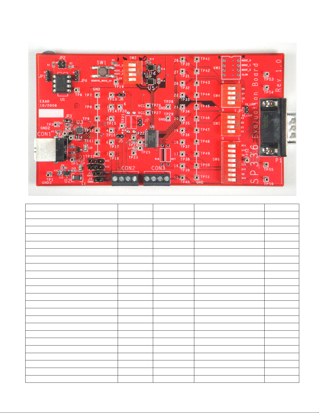
The SP336 Evaluation Board is designed to analyze the SP336 multi-protocol transceiver.
The evaluation board provides access points to all of the driver and receiver I/O pins so that the
user can measure electrical characteristics and waveforms of each signal. The evaluation board
also has a switch to allow the user to select the mode of operation and slew control.
Furthermore, the SP336 Evaluation Board provides the means to test both local and remote
driver/receiver loop-back.
This Manual is split into sections to give the user the information necessary to perform a
thorough evaluation of the SP336. The “Layout” section describes the I/O pins, jumpers and the
other components used on the evaluation board. The layout diagram is also covered. The “Using
the SP336 Evaluation Board” section details the configuration of the SP336 evaluation board for
parametric testing.
Page 2
2
Board Layout
Figure 1 – Evaluation Board Layout
Table 1
TEST POINT
WHERE
DEVICE
PAIR TEST POINT
SIGNAL
TP32
T1_IN
U6-26
TP44
GND
TP31
T2_IN
U6-27
TP43
GND
TP30
T3_IN
U6-28
TP42
GND
TP14
T4_IN
U6-1
TP8
GND
TP36
R1_OUT
U6-19
TP48
GND
TP35
R2_OUT
U6-20
TP50
GND
TP34
R3_OUT
U6-21
TP45
GND
TP33
R4_OUT
U6-22
TP41
GND
TP17
T1_OUT
U6-6
TP11
GND
TP18
T2_OUT
U6-7
TP12
GND
TP16
T3_OUT
U6-4
TP10
GND
TP15
T4_OUT
U6-3
TP9
GND
TP40
R1_IN
U6-15
TP47
GND
TP39
R2_IN
U6-16
TP51
GND
TP38
R3_IN
U6-17
TP49
GND
TP37
R3_IN
U6-18
TP46
GND
TP27, TP26
VCC
U6-5
TP28, TP29
GND
U6-8
TP24
V+
U6-10 (C3)
TP22 (C3)
TP25
V-
U6-14 (C4)
TP23 (C4)
J1-2 & J2-2
VCC
Board
VCC
TP53, TP54, TP54, & TP56
GND
Board
GND
J3-2 & J4-2
GND
Board
GND
Page 3
3
Table 2
Resistor
Header
Device
Mode Selected
R10
J7
U6-6&7
Mode 100
R11
J6
U6-3&4
Mode 010 & 100
R16
U6-15&16
Mode 101
R17
U6-17&18
Mode 011 & 101
Table 3
SW3-1
SW3-2
SW3-3
SW34
MODE_0
MODE_1
MODE_3
SLEW
0 0 0
x
Loopback TXin to
RXout
Txout & Rxin High
Impedance
0 0 1
x
RS-232 Mode
4T/4R RS232 Mode
0 1 0
x
Mixed Protocol, Half
Duplex
2T/2R RS232 Mode &
1T/1R RS-485
0 1 1
x
Mixed Protocol, Full
Duplex
2T/2R RS232 Mode &
1T/1R RS-485
1 0 0
x
RS-485/422 Half Duplex
2T/2R RS-485
1 0 1
x
RS-485/422 Full Duplex
2T/2R RS-485
1 1 0
x
Low Power, 4Rx Active
Driver at High
Impedance
1 1 1
x
Low Power Shutdown
All I/O at High
Impedance
x x x
0
RS-232 at 250kbps
RS-485 at 250Kbps
x x x
1
RS-232 at 1Mbps
RS-485 at 10Mbps
Note: Mode set for zero, SW3 to the Right
Mode set for one, SW3 to the Left
Page 4
4
Using the SP336 Evaluation Board
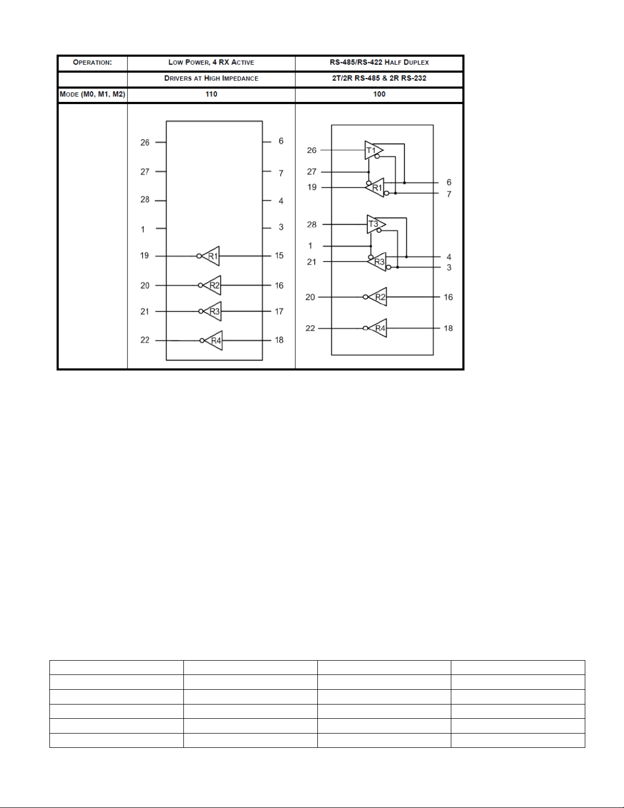
MODE CONFIGURATION
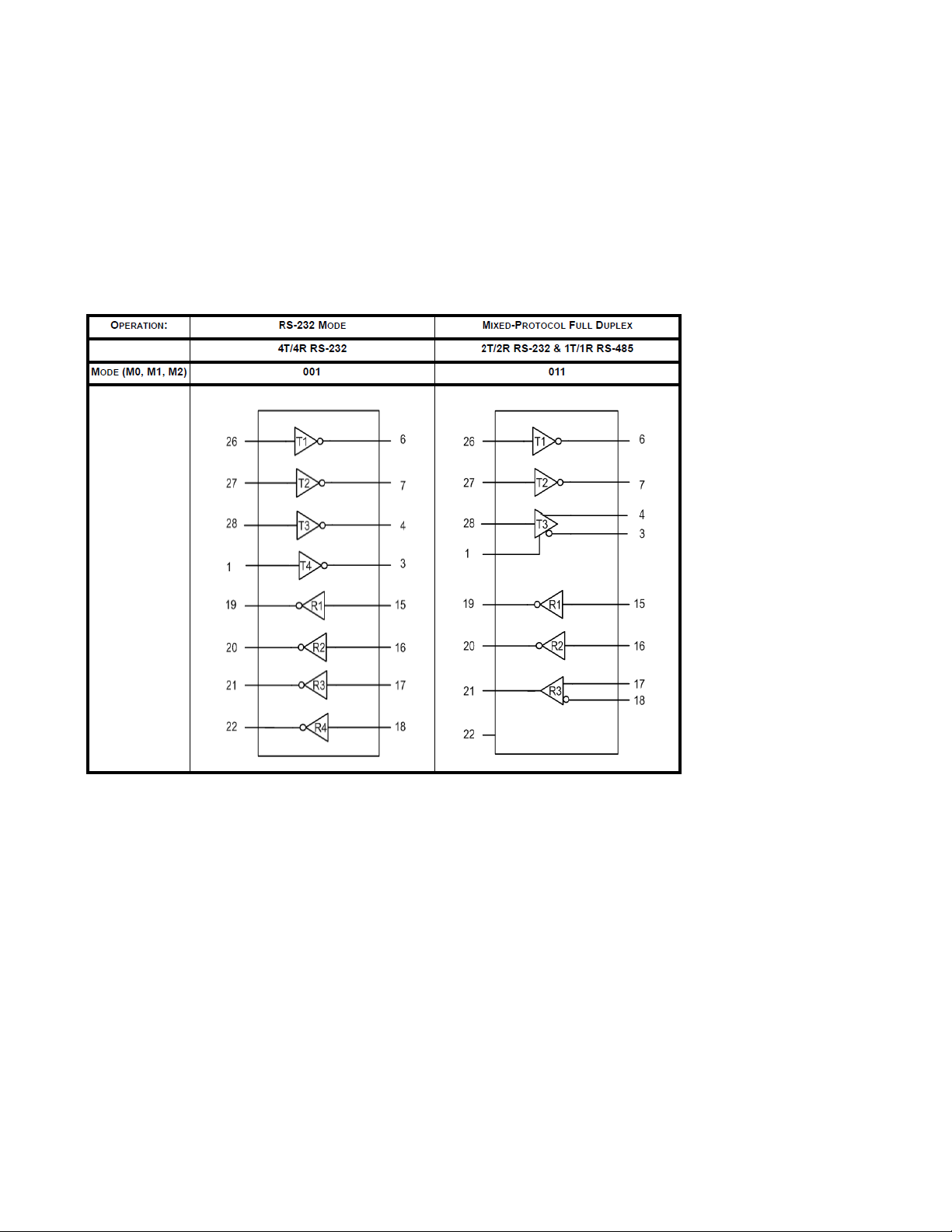
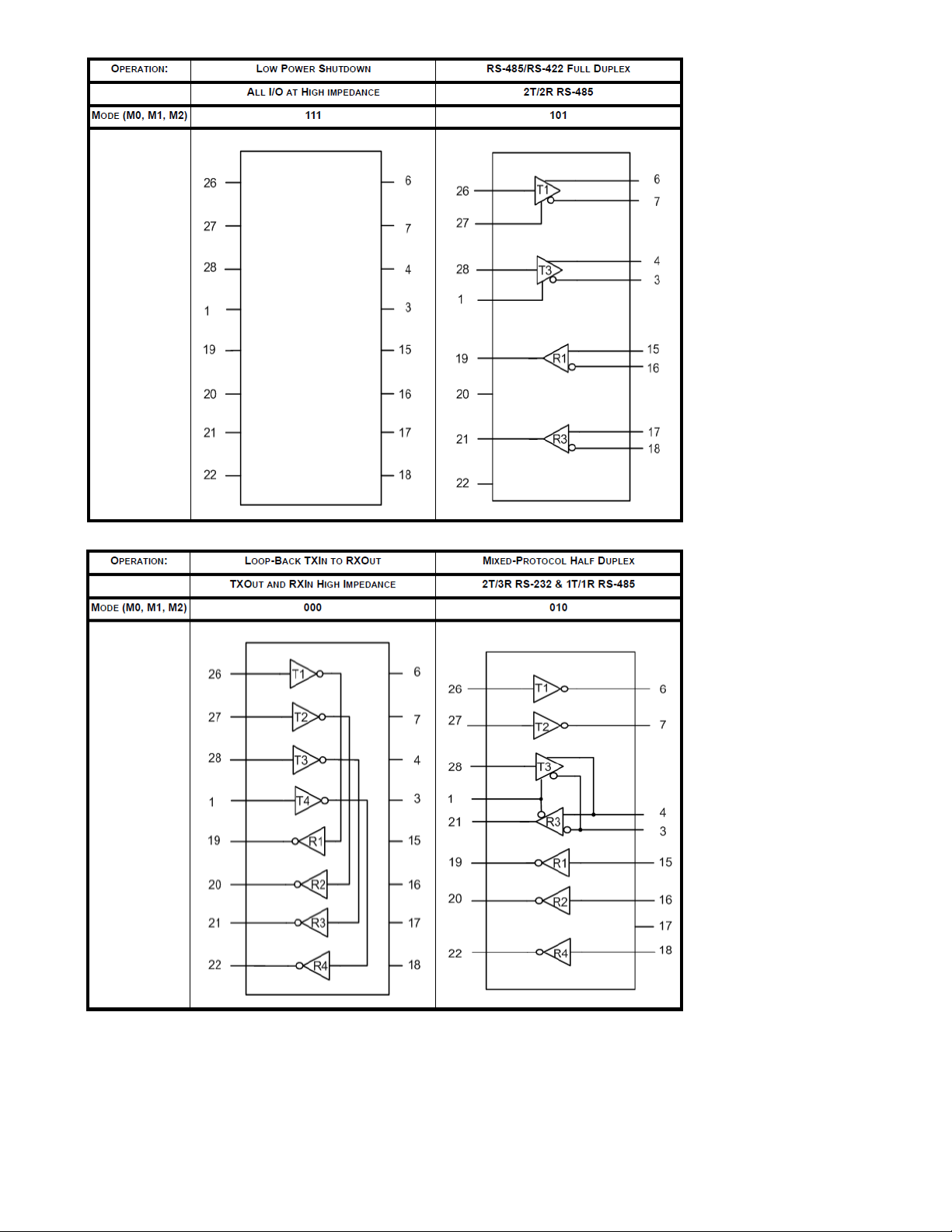
The SP336 uses a 3 bit decoder to define the protocol selected. The mode selection truth table
is shown in the data sheet and in Table 3. The SP336E supports eight distinct operating modes.
Modes are set using the three Mode-Configuration input pins M0, M1, and M2, which correspond
to SW3 (to the right is zero and to the left is one). The driver and receiver electrical
characteristics and the pin functions change depending on the mode selected.
Figure 1- Mode Configuration
Page 5
5
Page 6
6
Table 2 is a matrix describing all the possible modes for the SP366 and lists the jumper settings
for each mode. The Driver inputs, SLEW, MODE and the Loop back are all define an operating
mode. The modes are listed in the first column. The inputs to T1_In (TP32 & TP44), T2_In (TP31
& TP43), T3_In (TP30 & TP42) and T4_In (TP14 & TP8) can be made using the 50 Ohm
terminated resistor. Set the SP336 for the mode to be tested. Channels can also be connected
high or low individually by the test points mention above and reference in Table 1.
Slew rate control for the SP336E drivers is logic selectable using the SLEW pin which is
connected to SW3-4 “1”. Connecting SW3-4 (Left) provides high speed and no slew limiting
while SW3-4 “0” (Right) limits the driver slew rate.
Local loop back diagnostic mode for RS232 is provided “on chip” by using logic programmable
mode 000. Local loop back testing for RS485/422 mode is also provided on the evaluation board
and can be implemented using the headers (Sw3-1 is Mode 0, SW3-2 is Mode 1 & SW3-3 is
Mode 2). Set mode input logic to 101 to define RS485/422 mode. Follow Table 4 and jumper
from test point to test point to Loopback.
Reference to Table 4:
Table 4
Device
Signal
Device
Signal
U6-6
T1_out TP17
U6-15
R1_in TP40
U6-7
T2_out TP21
U6-16
R2_in TP39
U6-4
T1_out TP16
U6-17
R3_in TP38
U6-3
T1_out TP15
U6-18
R4_in TP37
Page 7
7
Refer to Table 1 for the desired inputs and outputs for loading. Loading the receiver outputs can
be done thru test points on Table 4. Remember that the receiver acts as one load when
connected to a driver output in a loop back configuration.
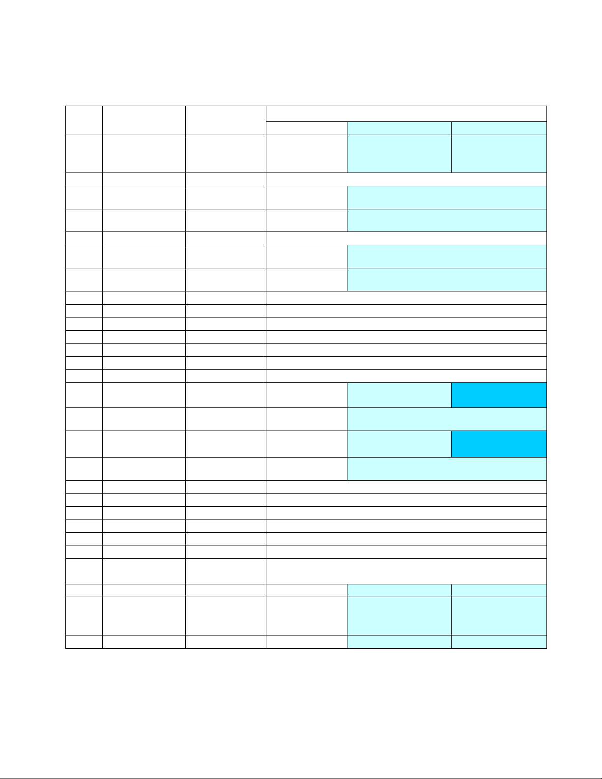
Table 5 – Pin Descriptions
Pin Functions
Pin
Name
Type
Single Ended
Full-Duplex
Half-Duplex
1
T4_In
TTL Input
T4 Driver Input
T3 Driver Enable
Active High
T3 Driver Enable
Active High, R3
Enable Active Low
2
Mode_1
TTL Input
Mode configuration pin 1
3
T4_Out
Bus Driver
T4 Driver
Output
T3(A) Output
4
T3_Out
Bus Driver
T3 Driver
Output
T3(B) Output
5
Vcc
Supply
Power Supply Voltage
6
T1_Out
Bus Driver
T1 Driver
Output
T1(A) Output
7
T2_Out
Bus Driver
T2 Driver
Output
T1(B) Output
8
GND
Supply
Ground
9
C1+
Pump
Positive terminal of positive flying capacitor
10
V+
Pump
Vdd of charge pump
11
C2+
Pump
Positive terminal of negative flying capacitor
12
C1-
Pump
Negative terminal of positive flying capacitor
13
C2-
Pump
Negative terminal of negative flying capacitor
14
V-
Pump
Vss of charge pump
15
R1_In
Bus Receiver
R1 Receiver
Input
R1(A) Receiver Input
Tri-State
16
R2_In
Bus Receiver
R2 Receiver
Input
R1(B) Receiver Input
17
R3_In
Bus Receiver
R3 Receiver
Input
R3(A) Receiver Input
Tri-State
18
R4_In
Bus Receiver
R4 Receiver
Input
R3(B) Receiver Input
19
R1_Out
TTL Output
Receiver 1 Output
20
R2_Out
TTL Output
Receiver 2 Output
21
R3_Out
TTL Output
Receiver 3 Output
22
R4_Out
TTL Input
Receiver 4 Output
23
Mode_2
TTL Input
Mode configuration pin 2
24
Mode_0
TTL Input
Mode configuration pin 0
25
SLEW
TTL Input
Slew Rate Control. Logic low input will limit driver slew from
either RS-232 or RS-485 to 250kbps
26
T1_In
TTL Input
T1 Driver Input
T1 Driver Input
T1 Driver Input
27
T2_In
TTL Input
T2 Driver Input
or T1 Driver
Enable
T1 Driver Enable
Active High
T1 Driver Enable
Active High, R1
Enable Active Low
28
T3_In
TTL Input
T3 Driver Input
T3 Driver Input
T3 Driver Input
 Loading...